

VISHAY
19232
e3
Pb
Pb-free
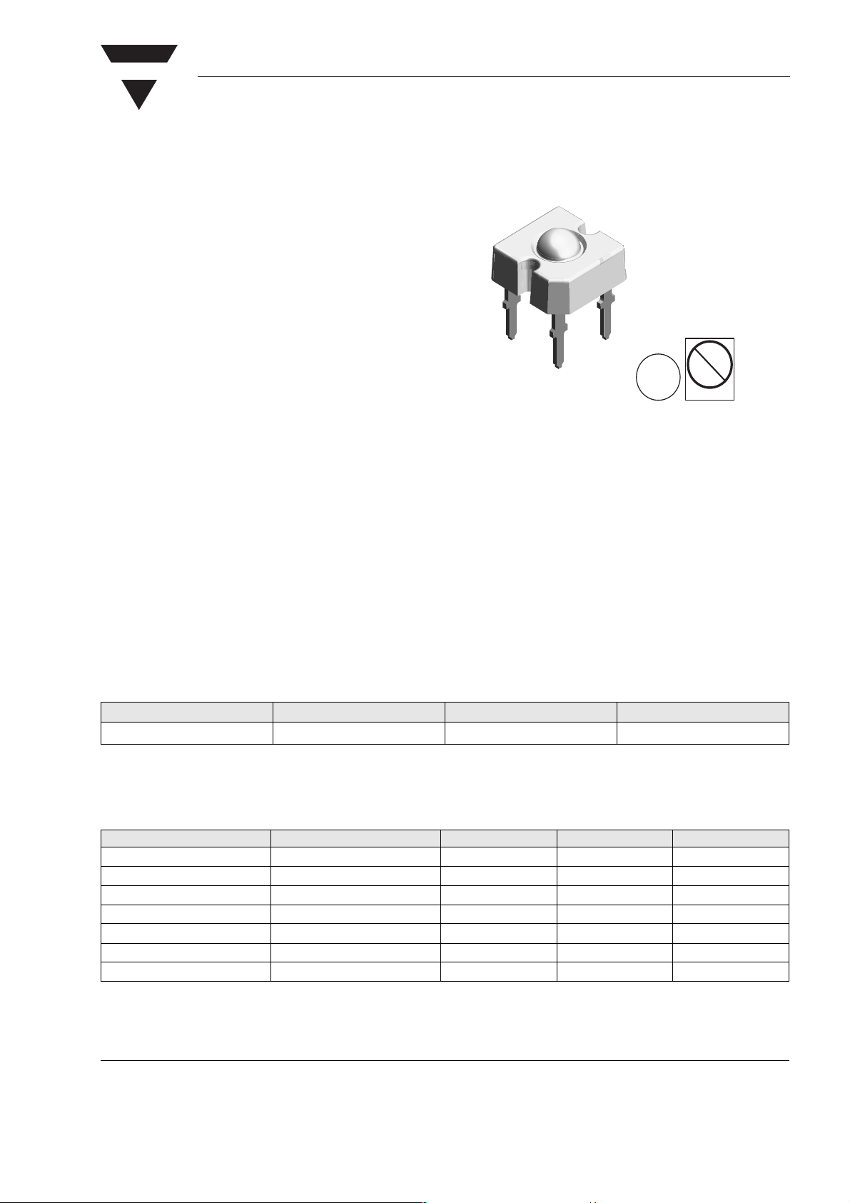
TELUX™ LED
Description
The TELUX™ series is a clear, non diffused LED for
high end applications where supreme luminous flux is
required.
It is designed in an industry standard 7.62 mm square
package utilizing highly developed InGaN technology.
The supreme heat dissipation of TELUX™ allows
applications at high ambient temperatures.
All packing units are binned for luminous flux and
color to achieve best homogenous light appearance
in application.
TLWW8600
Vishay Semiconductors
Features
• Lead-free device
• Utilizing InGaN technology
• High luminous flux
• Supreme heat dissipation: R
• High operating temperature: T
is 90 K/W
thJP
+ 100 °C
j
• Packed in tubes for automatic insertion
• Luminous flux and color categorized for each tube
Applications
Exterior lighting
Dashboard illumination
Tail-, Stop - and Turn Signals of motor vehicles
Replaces incandescent lamps
• Small mechanical tolerances allow precise usage
of external reflectors or lightguides
• ESD-withstand voltage:
> 1 kV acc. to MIL STD 883 D, Method 3015.7
Parts Table
Part Color, Luminous Intensity Angle of Half Intensity (±ϕ) Technology
TLWW8600 White, φ
> 630 mlm 30 ° InGaN / TAG on SiC
V
Absolute Maximum Ratings
T
= 25 °C, unless otherwise specified
amb
TLWW8600
Parameter Test condition Symbol Value Unit
Reverse voltage I
DC Forward current T
Surge forward current t
Power dissipation T
Junction temperature T
Operating temperature range T
Storage temperature range T
= 10 µAV
R
≤ 50 °C I
amb
≤ 10 µsI
p
≤ 50 °C P
amb
F
FSM
amb
stg
R
V
j
5V
50 mA
0.1 A
255 mW
100 °C
- 40 to + 100 °C
- 55 to + 100 °C
Document Number 83169
Rev. 1.5, 31-Aug-04
www.vishay.com
1
TLWW8600
VISHAY
Vishay Semiconductors
Parameter Test condition Symbol Val ue Unit
Soldering temperature t ≤ 5 s, 1.5 mm from body
T
sd
260 °C
preheat temperature
100 °C/ 30 sec.
Thermal resistance junction/
ambient
with cathode heatsink
of 70 mm
2
Thermal resistance junction/pin R
R
thJA
thJP
200 K/W
90 K/W
Optical and Electrical Characteristics
T
= 25 °C, unless otherwise specified
amb
White
TLWW8600
Parameter Test condition Symbol Min Ty p. Max Unit
Total flux I
Luminous intensity/Total flux I
Color temperature I
Angle of half intensity I
= 50 mA,
F
R
= 200 °K/W
thJA
= 50 mA,
F
= 200 °K/W
R
thJA
= 50 mA,
F
= 200 °K/W
R
thJA
= 50 mA,
F
= 200 °K/W
R
thJA
φ
V
I
V/φV
T
K
ϕ ± 30 deg
Total included angle 90 % of Total Flux Captured ϕ 75 deg
Forward voltage I
Reverse voltage I
Junction capacitance V
= 50 mA,
F
R
= 200 °K/W
thJA
= 10 µAV
R
= 0, f = 1 MHz C
R
V
F
R
j
630 1000 mlm
0.8 mcd/mlm
5500 K
4.3 5.2 V
510 V
50 pF
Chromaticity Coordinate Classification
Group X Y
min max min max
3a 0.29 0.3025 Y = 1.4x - 0.121 Y = 1.4x - 0.071
3b 0.3025 0.315 Y = 1.4x - 0.121 Y = 1.4x - 0.071
3c 0.29 0.3025 Y = 1.4x - 0.171 Y = 1.4x - 0.121
3d 0.3025 0.315 Y = 1.4x - 0.171 Y = 1.4x - 0.121
4a 0.315 0.3275 Y = 1.4x - 0.121 Y = 1.4x - 0.071
4b 0.3275 0.34 Y = 1.4x - 0.121 Y = 1.4x - 0.071
4c 0.315 0.3275 Y = 1.4x - 0.171 Y = 1.4x - 0.121
4d 0.3275 0.34 Y = 1.4x - 0.171 Y = 1.4x - 0.121
5a 0.34 0.3525 Y = 1.4x - 0.121 Y = 1.4x - 0.071
5b 0.3525 0.365 Y = 1.4x - 0.121 Y = 1.4x - 0.071
5c 0.34 0.3525 Y = 1.4x - 0.171 Y = 1.4x - 0.121
5d 0.3525 0.365 Y = 1.4x - 0.171 Y = 1.4x - 0.121
tolerance ± 0.005
www.vishay.com
2
Document Number 83169
Rev. 1.5, 31-Aug-04

VISHAY
TLWW8600
Vishay Semiconductors
Typical Characteristics (T
250
225
200
175
150
125
100
75
R
= 200 K/W
thJA
50
V
P - Power Dissipation ( mW )
25
0
08020 40 60 100 120
T
16066
- Ambient Temperature ( ° C)
amb
= 25 °C unless otherwise specified)
amb
Figure 1. Power Dissipation vs. Ambient Temperature for InGaN
60
50
40
30
20
F
10
I - Forward Current ( mA )
0
16067
= 200 K/W
R
thJA
08020 40 60 100 120
T
- Ambient Temperature ( ° C)
amb
100
90
80
70
60
50
40
30
20
% Total Luminous FluxR in K/W
10
0
0 2 5 50 75 100 125
16005
Total Included Angle (Degrees)
Figure 4. Percentage Total Luminous Flux vs. Total Included Angle
for 60 ° emission angle
230
220
210
200
190
thJA
180
170
160
0 50 100 150 200 250 300
16009
Cathode Padsize in mm
Padsize 8 mm
per Anode Pin
2
2
Figure 2. Forward Current vs. Ambient Temperature for InGaN
0°
v rel
I – Relative Luminous Intensity
16006
1.0
0.9
0.8
0.7
0.4 0.2 0 0.2 0.4
0.6
10° 20°
30°
40°
50°
60°
70°
80°
0.6
Figure 3. Rel. Luminous Intensity vs. Angular Displacement
for 60 ° emission angle
Document Number 83169
Rev. 1.5, 31-Aug-04
Figure 5. Thermal Resistance Junction Ambient vs. Cathode
Padsize
100
90
White
80
70
60
50
40
30
20
F
I - Forward Current ( mA )
10
0
2.5 3.0 3.5 4.0 4.5 5.0 5.5
16062
VF- Forward Voltage ( V )
Figure 6. Forward Current vs. Forward Voltage
www.vishay.com
3

TLWW8600
Vishay Semiconductors
VISHAY
1.8
1.6
White
IF=50mA
1.4
1.2
1.0
0.8
0.6
- Relative Luminous Flux
0.4
V rel
Φ
0.2
0.0
-40 -20 0 20 4 0 60 80 100
16065
T
- Ambient Temperature ( ° C)
amb
Figure 7. Rel. Luminous Flux vs. Ambient Temperature
White
1.0
1.2
1.1
1.0
0.9
0.8
0.7
0.6
0.5
0.4
0.3
0.2
V rel
I - Relative Luminous Intensity
0.1
0.0
400 450 500 550 600 650 700 750 800
16071
ı
λ
- Wavelength ( nm )
Figure 10. Relative Intensity vs. Wavelength
0.345
0.340
X
0.335
0.330
0.325
White
Y
IF=50mAWhite
Spec
I - Specific Luminous Flux
0.1
1 1 0 100
16063
IF- Forward Current ( mA )
Figure 8. Specific Luminous Flux vs. Forward Current
10.00
White
1.00
0.10
V rel
I - Relative Luminous Flux
0.01
1 10 100
I
16064
- Forward Current ( mA )
F
Figure 9. Relative Luminous Flux vs. Forward Current
0.320
f - Chromaticity coordinate shift (x,y)
0.315
0605040302010
16198
I
- Forward Current ( mA )
F
Figure 11. Chromaticity Coordinate Shift vs. Forward Current
0.44
0.42
0.40
0.38
0.36
0.34
0.32
0.30
0.28
Y and Y’ Coordinates
0.26
4b
4a
3b
3a
3d
3c
4d
4c
5b
5a
5d
5c
0.24
0.22
0.28 0.29 0.30 0.31 0.32 0.33 0.34 0.35 0.36 0.37
19037
X Coordinates
Figure 12. Coordinates of Colorgroups
www.vishay.com
4
Document Number 83169
Rev. 1.5, 31-Aug-04

VISHAY
Package Dimensions in mm
TLWW8600
Vishay Semiconductors
Document Number 83169
Rev. 1.5, 31-Aug-04
16004
www.vishay.com
5

TLWW8600
VISHAY
Vishay Semiconductors
Ozone Depleting Substances Policy Statement
It is the policy of Vishay Semiconductor GmbH to
1. Meet all present and future national and international statutory requirements.
2. Regularly and continuously improve the performance of our products, processes, distribution and
operatingsystems with respect to their impact on the health and safety of our employees and the public, as
well as their impact on the environment.
It is particular concern to control or eliminate releases of those substances into the atmosphere which are
known as ozone depleting substances (ODSs).
The Montreal Protocol (1987) and its London Amendments (1990) intend to severely restrict the use of ODSs
and forbid their use within the next ten years. Various national and international initiatives are pressing for an
earlier ban on these substances.
Vishay Semiconductor GmbH has been able to use its policy of continuous improvements to eliminate the
use of ODSs listed in the following documents.
1. Annex A, B and list of transitional substances of the Montreal Protocol and the London Amendments
respectively
2. Class I and II ozone depleting substances in the Clean Air Act Amendments of 1990 by the Environmental
Protection Agency (EPA) in the USA
3. Council Decision 88/540/EEC and 91/690/EEC Annex A, B and C (transitional substances) respectively.
Vishay Semiconductor GmbH can certify that our semiconductors are not manufactured with ozone depleting
substances and do not contain such substances.
We reserve the right to make changes to improve technical design
and may do so without further notice.
Parameters can vary in different applications. All operating parameters must be validated for each
customer application by the customer. Should the buyer use Vishay Semiconductors products for any
unintended or unauthorized application, the buyer shall indemnify Vishay Semiconductors against all
claims, costs, damages, and expenses, arising out of, directly or indirectly, any claim of personal
damage, injury or death associated with such unintended or unauthorized use.
Vishay Semiconductor GmbH, P.O.B. 3535, D-74025 Heilbronn, Germany
Telephone: 49 (0)7131 67 2831, Fax number: 49 (0)7131 67 2423
www.vishay.com
6
Document Number 83169
Rev. 1.5, 31-Aug-04
 Loading...