

VISHAY
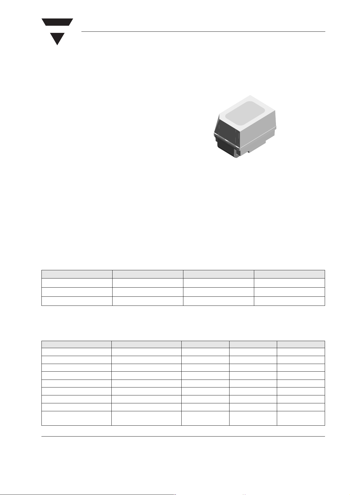
MiniLED Ultrabright
Description
The new MiniLED Series have been designed in a
small white SMT package. The feature of the device
is the very small package 2.3 mm x 1.3 mm x 1.4 mm.
The MinLED is an obvious solution for small-scale,
high-power products that are expected to work reliability in an arduous environment. This is often the
case in automotive and industrial application.
TLME / F / K2300
Vishay Semiconductors
Features
• SMD LEDs with exceptional brightness
• Luminous intensity categorized
• Compatible with automatic placement equipment
• IR reflow soldering
• Available in 8 mm tape
• Low profile package
• Non-diffused lens: Excellent for coupling to light
pipes and backlighting
• Low power consumption
• Luminous intensity ratio in one packing unit
I
Vmax/IVmin
≤ 2.0, optional ≤ 1.6
Parts Table
Part Color, Luminous Intensity Angle of Half Intensity (±ϕ) Technology
TLMK2300 Red, I
TLMF2300 Orange, I
TLME2300 Yellow, I
= 80 mcd (typ.) 60 ° AlInGaP on GaAs
V
= 120 mcd (typ.) 60 ° AlInGaP on GaAs
V
= 120 mcd (typ.) 60 ° AlInGaP on GaAs
V
16906
Applications
Automotive: Backlighting in dashboards and switches
Telecommunication: Indicator and backlighting in
telephone and fax
Indicator and backlight for audio and video equipment
Indicator and backlight in office equipment
Flat backlight for LCDs, switches and symbols
Absolute Maximum Ratings
T
= 25 °C, unless otherwise specified
amb
TLMK230. ,TLMF230. ,TLME230.
Parameter Test condition Symbol Value Unit
Reverse voltage V
DC Forward current T
Surge forward current t
Power dissipation T
Junction temperature T
Operating temperature range T
Storage temperature range T
Soldering temperature according to IPC 9501 T
Thermal resistance junction/
ambient
Document Number 83200
Rev. 1.6, 17-Jun-04
≤ 80 °C I
amb
≤ 10 µsI
p
≤ 80 °C P
amb
mounted on PC board
(pad size > 5 mm
2
)
R
F
FSM
amb
stg
sd
thJA
R
V
j
5V
30 mA
0.1 A
80 mW
125 °C
- 40 to + 100 °C
- 40 to + 100 °C
245 °C
580 K/W
www.vishay.com
1
TLME / F / K2300
Vishay Semiconductors
Optical and Electrical Characteristics
T
= 25 °C, unless otherwise specified
amb
Red
TLMK230.
Parameter Test condition Symbol Min Ty p. Max Unit
Luminous intensity
1)
Dominant wavelength I
Peak wavelength I
Angle of half intensity I
Forward voltage I
Reverse voltage I
Junction capacitance V
1)
in one Packing Unit I
Vmax/IVmin
Orange
TLMF230.
Parameter Test condition Symbol Min Ty p. Max Unit
Luminous intensity
Dominant wavelength I
Peak wavelength I
Angle of half intensity I
Forward voltage I
Reverse voltage I
Junction capacitance V
1)
in one Packing Unit I
1)
Vmax/IVmin
IF = 20 mA I
= 20 mA λ
F
= 20 mA λ
F
= 20 mA ϕ ± 60 deg
F
= 20 mA V
F
= 10 µAV
R
= 0, f = 1 MHz C
R
≤ 2.0
IF = 20 mA I
= 20 mA λ
F
= 20 mA λ
F
= 20 mA ϕ ± 60 deg
F
= 20 mA V
F
= 10 µAV
R
= 0, f = 1 MHz C
R
≤ 2.0
VISHAY
V
d
p
F
R
j
V
d
p
F
R
j
32 80 mcd
630 nm
643 nm
1.9 2.6 V
5V
15 pF
50 120 mcd
598 605 611 nm
610 nm
2.0 2.6 V
5V
15 pF
Yellow
TLME230.
Parameter Test condition Symbol Min Ty p. Max Unit
Luminous intensity
Dominant wavelength I
Peak wavelength I
Angle of half intensity I
Forward voltage I
Reverse voltage I
Junction capacitance V
1)
in one Packing Unit I
www.vishay.com
2
1)
Vmax/IVmin
IF = 20 mA I
= 20 mA λ
F
= 20 mA λ
F
= 20 mA ϕ ± 60 deg
F
= 20 mA V
F
= 10 µAV
R
= 0, f = 1 MHz C
R
V
d
p
F
R
j
50 120 mcd
581 588 594 nm
590 nm
2.0 2.6 V
5V
15 pF
≤ 2.0
Document Number 83200
Rev. 1.6, 17-Jun-04
VISHAY
TLME / F / K2300
Vishay Semiconductors
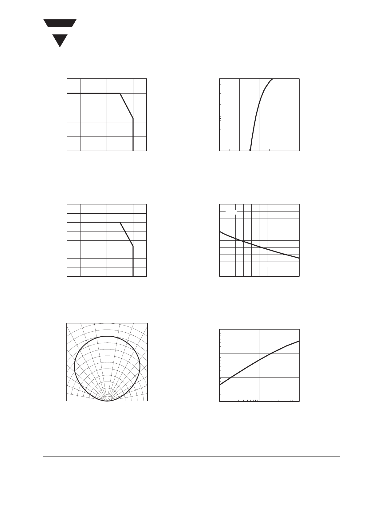
Typical Characteristics (T
100
80
60
40
20
V
P –Power Dissipation (mW)
0
0 20406080100120
17523
T
– Ambient Temperature ( qC )
amb
= 25 °C unless otherwise specified)
amb
Figure 1. Power Dissipation vs. Ambient Temperature
40
35
30
25
20
15
10
F
I –Forward Current ( mA )
5
0
0 20406080100120
17524
T
– Ambient Temperature ( qC )
amb
100
Red
10
F
I - Forward Current ( mA )
1
1.0 1.5 2.0 2.5 3.0
17509
VF- Forward V oltage(V)
Figure 4. Forward Current vs. Forward Voltage
2.0
1.8
Red
1.6
1.4
1.2
1.0
0.8
0.6
0.4
Vrel
0.2
I –Relative Luminous Intensity
0.0
0 1020304050607080 90100
T
17510
– Ambient Temperature ( qC )
amb
IF = 20 mA
Figure 2. Forward Current vs. Ambient Temperature
0°
10° 20°
30°
40°
1.0
Vre l
I - Relative Luminous Intensity
95 10319
0.9
0.8
0.7
0.4 0.2 0 0.2 0.4
0.6
50°
60°
70°
80°
0.6
Figure 3. Rel. Luminous Intensity vs. Angular Displacement
Document Number 83200
Rev. 1.6, 17-Jun-04
Figure 5. Rel. Luminous Intensity vs. Ambient Temperature
10
Red
1
0.1
Vrel
I - Relative Luminous Intensity
0.01
1 10 100
17511
IF- Forward Current ( mA )
Figure 6. Relative Luminous Intensity vs. Forward Current
www.vishay.com
3
TLME / F / K2300
Vishay Semiconductors
VISHAY
1.2
1.1
Red
1.0
0.9
0.8
0.7
0.6
0.5
0.4
0.3
rel
I – Relative Intensity
0.2
0.1
0.0
600 610620 630 640 650 660 670 680 690 700
17512
O – Wavelength ( nm )
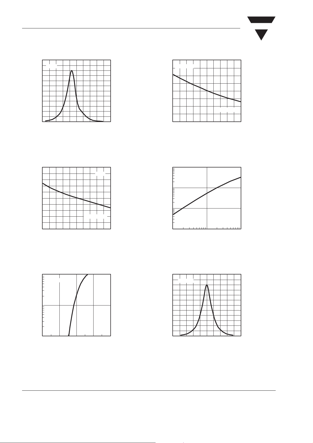
Figure 7. Relative Intensity vs. Wavelength
2.10
2.05
2.00
1.95
1.90
1.85
1.80
1.75
F
1.70
V – Forward Voltage ( V )
1.65
1.60
0 1020304050607080 90100
T
17513
– Ambient Temperature ( qC )
amb
Red
IF = 20 mA
1.6
Orange
1.4
1.2
1.0
0.8
0.6
0.4
Vrel
0.2
I – Relative Luminous Intensity
0.0
0 1020304050607080 90100
T
17504
– Ambient Temperature ( qC )
amb
IF = 20 mA
Figure 10. Rel. Luminous Intensity vs. Ambient Temperature
10
Orange
1
0.1
Vrel
I - Relative Luminous Intensity
0.01
1 10 100
17505
IF- Forward Current ( mA )
Figure 8. Forward Voltage vs. Ambient Temperature
100
Orange
10
F
I - Forward Current ( mA )
1
1.0 1.5 2.0 2.5 3.0
17503
VF- Forward V oltage(V)
Figure 9. Forward Current vs. Forward Voltage
www.vishay.com
4
Figure 11. Relative Luminous Intensity vs. Forward Current
1.2
1.1
Orange
1.0
0.9
0.8
0.7
0.6
0.5
0.4
0.3
rel
I – Relative Intensity
0.2
0.1
0.0
560 570580 590 600 610 620 630 640 650 660
17506
O – Wavelength ( nm )
Figure 12. Relative Intensity vs. Wavelength
Document Number 83200
Rev. 1.6, 17-Jun-04

VISHAY
TLME / F / K2300
Vishay Semiconductors
2.10
2.05
2.00
1.95
1.90
1.85
1.80
1.75
F
1.70
V – Forward Voltage ( V )
1.65
1.60
0 1020304050607080 90100
T
17507
– Ambient Temperature ( qC )
amb
Orange
IF = 20 mA
Figure 13. Forward Voltage vs. Ambient Temperature
100
Yellow
10
F
I - Forward Current ( mA )
1
1.0 1.5 2.0 2.5 3.0
95 10878y
VF- Forward V oltage(V)
10
Yellow
1
0.1
Vrel
I - Relative Luminous Intensity
0.01
1 10 100
17501
IF- Forward Current ( mA )
Figure 16. Relative Luminous Intensity vs. Forward Current
1.2
1.1
Yellow
1.0
0.9
0.8
0.7
0.6
0.5
0.4
0.3
rel
I – Relative Intensity
0.2
0.1
0.0
550 560570 580 590 600 610 620 630 640 650
95 10881y
l – Wavelength ( nm )
Figure 14. Forward Current vs. Forward Voltage
1.6
Yellow
1.4
1.2
1.0
0.8
0.6
0.4
Vrel
0.2
I – Relative Luminous Intensity
0.0
0 1020304050607080 90100
T
17508
– Ambient Temperature ( qC )
amb
IF = 20 mA
Figure 15. Rel. Luminous Intensity vs. Ambient Temperature
Document Number 83200
Rev. 1.6, 17-Jun-04
Figure 17. Relative Intensity vs. Wavelength
2.15
2.10
2.05
2.00
1.95
1.90
1.85
1.80
F
1.75
V – Forward Voltage ( V )
1.70
1.65
0 1020304050607080 90100
T
17502
– Ambient Temperature ( qC )
amb
Yellow
IF = 20 mA
Figure 18. Forward Voltage vs. Ambient Temperature
www.vishay.com
5

TLME / F / K2300
Vishay Semiconductors
Package Dimensions in mm
VISHAY
www.vishay.com
6
16892
Document Number 83200
Rev. 1.6, 17-Jun-04

VISHAY
Reel Dimensions
TLME / F / K2300
Vishay Semiconductors
Document Number 83200
Rev. 1.6, 17-Jun-04
16938
www.vishay.com
7

TLME / F / K2300
Vishay Semiconductors
Tape Dimensions
VISHAY
Leader and Trailer
Trailer Leader
no devices no devices
min. 200 min. 400
16939
devices
StartEnd
96 11818
GS08 = 3000 pcs
www.vishay.com
8
Document Number 83200
Rev. 1.6, 17-Jun-04

VISHAY
TLME / F / K2300
Vishay Semiconductors
Cover Tape Peel Strength
According to DIN EN 60286-3
0.1 to 1.3 N
300 ± 10 mm/min
165 ° - 180 ° peel angle
Label
Standard bar code labels for finished goods
The standard bar code labels are product labels and
used for identification of goods. The finished goods
are packed in final packing area. The standard packing units are labeled with standard bar code labels
before transported as finished goods to warehouses.
The labels are on each packing unit and contain
Vishay Semiconductor GmbH specific data.
Vishay Semiconductor GmbH standard bar code product label (finished goods)
Plain Writing Abbreviation
Item-Description
Item-Number
Selection-Code
LOT-/ Serial-Number
Data-Code
Plant-Code
Quantity
Accepted by:
Packed by:
Mixed Code Indicator
Origin
–
INO
SEL
BATCH
COD
PTC
QTY
ACC
PCK
MIXED CODE
xxxxxxx
+
Company Logo
Length
18
8
3
10
3 (YWW)
2
8
–
–
–
Long Bar Code Top Type
Item-Number
Plant-Code
Sequence-Number
Quantity
Total Length
Short Bar Code Bottom
Selection–Code
Data-Code
Batch-Number
Filter
Total Length
Length
N8
N
X
N
–
Type
X3
N
X
–
–
2
3
8
21
Length
3
10
1
17
16942
Document Number 83200
Rev. 1.6, 17-Jun-04
www.vishay.com
9

TLME / F / K2300
Vishay Semiconductors
Dry Packing
The reel is packed in an anti-humidity bag to protect
the devices from absorbing moisture during transportation and storage.
Aluminium bag
Label
Reel
15973
Final Packing
The sealed reel is packed into a cardboard box. A
secondary cardboard box is used for shipping purposes.
Recommended Method of Storage
Dry box storage is recommended as soon as the aluminium bag has been opened to prevent moisture
absorption. The following conditions should be
observed, if dry boxes are not available:
• Storage temperature 10 °C to 30 °C
• Storage humidity ≤ 60 % RH max.
After more than 1 year under these conditions mois-
ture content will be too high for reflow soldering.
In case of moisture absorption, the devices will
recover to the former condition by drying under the
following condition:
192 hours at 40 °C + 5 °C/ -0 °C and < 5 % RH
(dry air/ nitrogen) or
96 hours at 60 °C +5 °C and < 5 % RH for all device
containers or
24 hours at 100 °C +5 °C not suitable for reel
or tubes.
An EIA JEDEC Standard JESD22-A112 Level 2 label
is included on all dry bags.
VISHAY
17028
Example of JESD22-A112 Level 2 label
ESD Precaution
Proper storage and handling procedures should be
followed to prevent ESD damage to the devices especially when they are removed from the Antistatic
Shielding Bag. Electro-Static Sensitive Devices warning labels are on the packaging.
Vishay Semiconductors Standard Bar-Code Labels
The Vishay Semiconductors standard bar-code labels
are printed at final packing areas. The labels are on
each packing unit and contain Vishay Semiconductors specific data.
www.vishay.com
10
Document Number 83200
Rev. 1.6, 17-Jun-04

VISHAY
TLME / F / K2300
Vishay Semiconductors
Assembly Instructions
Reflow Soldering
• Reflow soldering must be done within 1 year stored
under max. 30 °C, 60 % RH after opening envelop
• Recommended soldering paste (composition: SN 63
%, Pb 37 %) Melting temperature 178 °C to 192 °C
• Apply solder paste to the specified soldering pads,
by using a dispenser or by screen printing.
• Recommended thickness of metal mask is 0.2 mm
for screen printing.
• The recommended reflow furnace is a combinationtype with upper and lower heaters.
• Set the furnace temperatures for pre-heating and
heating in accordance with the reflow temperature
profile as shown below. Excercise extreme care to
keep the maximum temperature below 230 °C. The
following temperature profile means the tempera ture
at the device surface. Since temperature differ ence
occurs between the work and the surface of the circuit
board depending on the pes of circuit board or reflow
furnace, the operating conditions should be verified
prior to start of operation.
• Handling after reflow should be done only after the
work surface has been cooled off.
Manual Soldering
• Use the 6/4 solder or the solder containing silver.
• Use a soldering iron of 25 W or smaller. Adjust the
temperature of the soldering iron below 300 °C.
• Finish soldering within three seconds.
• Handle products only after the temperature is cooled
off.
Cleaning
• Perform cleaning after soldering strictly in conformance to the following conditions:
Cleaning agent:
2-propanol (isopropyl alcohol)
Commercially available grades (industrial use) should
be used.
Demineralized or distilled water having a resistivity of
not less than 500 mΩ corresponding to a conductivity
of 2 mS/m.
• Temperature and time: 30 seconds under the temperature below 50 °C or 3 minutes below 30 °C.
• Ultrasonic cleaning: Below 20 W.
Reflow Solder Profile
240
220
200
180
160
q
140
120
100
80
Temperature ( C )
60
40
20
0
0 50 100 150 200 250 300 350
2 qC - 4 qC/s
120 s - 180 s
2 qC - 4 qC/s
Time ( s )
90 s max
10 s max.
@ 230 qC
16944
Document Number 83200
Rev. 1.6, 17-Jun-04
www.vishay.com
11

TLME / F / K2300
VISHAY
Vishay Semiconductors
Ozone Depleting Substances Policy Statement
It is the policy of Vishay Semiconductor GmbH to
1. Meet all present and future national and international statutory requirements.
2. Regularly and continuously improve the performance of our products, processes, distribution and
operatingsystems with respect to their impact on the health and safety of our employees and the public, as
well as their impact on the environment.
It is particular concern to control or eliminate releases of those substances into the atmosphere which are
known as ozone depleting substances (ODSs).
The Montreal Protocol (1987) and its London Amendments (1990) intend to severely restrict the use of ODSs
and forbid their use within the next ten years. Various national and international initiatives are pressing for an
earlier ban on these substances.
Vishay Semiconductor GmbH has been able to use its policy of continuous improvements to eliminate the
use of ODSs listed in the following documents.
1. Annex A, B and list of transitional substances of the Montreal Protocol and the London Amendments
respectively
2. Class I and II ozone depleting substances in the Clean Air Act Amendments of 1990 by the Environmental
Protection Agency (EPA) in the USA
3. Council Decision 88/540/EEC and 91/690/EEC Annex A, B and C (transitional substances) respectively.
Vishay Semiconductor GmbH can certify that our semiconductors are not manufactured with ozone depleting
substances and do not contain such substances.
We reserve the right to make changes to improve technical design
and may do so without further notice.
Parameters can vary in different applications. All operating parameters must be validated for each
customer application by the customer. Should the buyer use Vishay Semiconductors products for any
unintended or unauthorized application, the buyer shall indemnify Vishay Semiconductors against all
claims, costs, damages, and expenses, arising out of, directly or indirectly, any claim of personal
damage, injury or death associated with such unintended or unauthorized use.
Vishay Semiconductor GmbH, P.O.B. 3535, D-74025 Heilbronn, Germany
Telephone: 49 (0)7131 67 2831, Fax number: 49 (0)7131 67 2423
www.vishay.com
12
Document Number 83200
Rev. 1.6, 17-Jun-04
 Loading...