

VISHAY
e3
Pb
Pb-free
19219
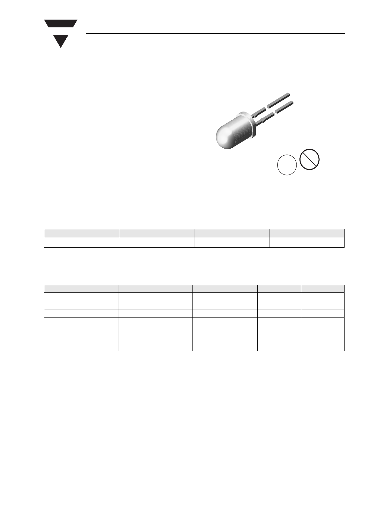
Blinking LED in ∅ 5 mm Plastic Package
Features
• Plastic case, colored diffuse
• Vibration resistant
• Built-in blink-function P-MOS IC f ≈ 3 Hz
• Supply voltage V
• Wide viewing angle ϕ = ± 40 °
• Cycle start in lighted phase
• Built-in current limiter
• Lead-free device
Applications
Blink function display
= 5 V
S
TLBR5410
Vishay Semiconductors
Parts Table
Part Color, Luminous Intensity Angle of Half Intensity (±ϕ) Technology
TLBR5410 Red, I
> 1 mcd 40 ° GaAsP on GaAsP/P-MOS
V
Absolute Maximum Ratings
T
= 25 °C, unless otherwise specified
amb
TLBR5410
Parameter Test condition Symbol Val ue Unit
Reverse voltage Pin +V
Supply voltage Pin +V
Total power dissipation T
Junction temperature T
Operating temperature range T
Storage temperature range T
Soldering temperature t ≤ 5 s, 2 mm from case T
S
S
≤ 70 °C P
amb
V
V
amb
stg
R
S
tot
j
sd
0.4 V
7V
200 mW
100 °C
- 40 to + 70 °C
- 55 to + 100 °C
260 °C
Document Number 83000
Rev. 1.4, 30-Aug-04
www.vishay.com
1

TLBR5410
Vishay Semiconductors
Optical and Electrical Characteristics
T
= 25 °C, unless otherwise specified
amb
Red
TLBR5410
Parameter Test condition Symbol Min Ty p. Max Unit
Luminous intensity
1)
Peak wavelength V
Spectral line half width V
Angle of half intensity V
Supply voltage range V
Supply current V
Blink frequency T
ON/OFF-ratio t
1)
in one Packing Unit I
Vmin/IVmax
VS = 5 V I
= 5 V λ
S
= 5 V ∆λ 20 nm
S
= 5 V ϕ ± 40 deg
S
= 5 V V
S
= 5 V I
S
= 25 °C f
amb
T
= (- 40 to + 70) °C f
amb
≤ 0.5
V
p
S
Son
I
Soff
bl
bl
on/toff
VISHAY
11.6 mcd
640 nm
4.75 7 V
10 30 mA
2mA
1.3 5.2 Hz
1.1 7.2 Hz
33 to 67 %
Typical Characteristics (T
500
400
VS=7V
300
200
VS=5V
V
100
P – Power Dissipation ( mW)
0
–40 –20 0 20 80
95 10000
T
IF=56mA
IF=40mA
IF=30mA
IF=20mA
40 60
– Ambient Temperature (°C )
amb
= 25 °C unless otherwise specified)
amb
Figure 1. Power Dissipation vs. Ambient Temperature
100
10
8
6
4
S
V – Supply Voltage ( V)
2
0
–40 –20 0 20 80
T
95 10001
– Ambient Temperature(°C )
amb
40 60
Figure 2. Supply Voltage vs. Ambient Temperature
100
www.vishay.com
2
Document Number 83000
Rev. 1.4, 30-Aug-04

VISHAY
TLBR5410
Vishay Semiconductors
50
40
30
20
Light–on Phase ( mA )
10
Fon
I – Forward Current during
0
024 6
95 10002
V
– Supply Voltage(V)
S
8
Figure 3. Forward Current (Light On) vs. Supply Voltage
50
VS=7V
40
A)
30
20
Light–on Phase ( m
VS=5V
10
Fon
I – Forward Current during
0
–40 –20 0 20 80
T
– Ambient Temperature(°C )
95 10003
amb
40 60
100
3.8
3.6
3.4
3.2
3.0
bl on
V – Blinking Threshold Voltage (V )
2.8
–40 –20 0 20 80
T
95 10005
– Ambient Temperature(°C )
amb
40 60
100
Figure 6. Blinking Threshold Voltage vs. Amb. Temperature
10
8
6
4
bl
2
f – Blinking Frequency ( Hz )
0
8
95 10008
4
56 7
– Supply Voltage(V)
V
S
Figure 4. Forward Current (Light On) vs. Amb. Temperature
2.0
A)
1.6
1.2
VS=7V
0.8
VS=5V
0.4
during Light–off Phase ( m
F off
I – Forward Current
0
–40 –20 0 20 80
T
95 10004
– Ambient Temperature( °C )
amb
40 60
100
Figure 5. Forward Current (Light Off) vs. Amb. Temperature
Document Number 83000
Rev. 1.4, 30-Aug-04
Figure 7. Blinking Frequency vs. Supply Voltage
10
8
6
4
bl
2
f – Blinking Frequency ( Hz )
0
–40 –20 0 20 80
T
95 10009
– Ambient Temperature(°C )
amb
40 60
100
Figure 8. Blinking Frequency vs. Ambient Temperature
www.vishay.com
3

TLBR5410
Vishay Semiconductors
VISHAY
0.60
0.55
0.50
p
t /T – Duty Cycle
0.45
0.40
456 7
V
95 10010
– Supply Voltage(V)
S
Figure 9. Duty Cycle vs. Supply Voltage
0.60
0.55
0.50
p
t /T – Duty Cycle
0.45
3
2.5
2
1.5
1
VS=5V
0.5
v rel
I – Relative Luminous Intensity
0
8
–40 –20 0 20 80
T
95 10007
– Ambient Temperature (°C )
amb
40 60
100
Figure 12. Relative Luminous Intensity vs. Amb. Temperature
1.2
Red
1.0
0.8
0.6
0.4
rel
I – Relative Intensity
0.2
0.40
–40 –20 0 20 80
– Ambient Temperature ( °C )
95 10011
T
amb
40 60
Figure 10. Duty Cycle vs. Ambient Temperature
10
1
V
I – Luminous Intensity ( mcd )
0.1
0
95 10006
24 6
V
– Supply Voltage(V)
S
Figure 11. Luminous Intensity vs. Supply Voltage
100
8
0.0
550 590 630 670 710 750
17521
l – Wavelength ( nm )
Figure 13. Relative Intensity vs. Wavelength
0°
10°20
°
30°
40°
1.0
v rel
I – Relative Luminous Intensity
95 10013
0.9
0.8
0.7
0.4 0.2 0 0.2 0.4
0.6
50°
60°
70°
80°
0.6
Figure 14. Rel. Luminous Intensity vs. Angular Displacement
www.vishay.com
4
Document Number 83000
Rev. 1.4, 30-Aug-04

VISHAY
Package Dimensions in mm
TLBR5410
Vishay Semiconductors
95 11264
Document Number 83000
Rev. 1.4, 30-Aug-04
www.vishay.com
5

TLBR5410
VISHAY
Vishay Semiconductors
Ozone Depleting Substances Policy Statement
It is the policy of Vishay Semiconductor GmbH to
1. Meet all present and future national and international statutory requirements.
2. Regularly and continuously improve the performance of our products, processes, distribution and
operatingsystems with respect to their impact on the health and safety of our employees and the public, as
well as their impact on the environment.
It is particular concern to control or eliminate releases of those substances into the atmosphere which are
known as ozone depleting substances (ODSs).
The Montreal Protocol (1987) and its London Amendments (1990) intend to severely restrict the use of ODSs
and forbid their use within the next ten years. Various national and international initiatives are pressing for an
earlier ban on these substances.
Vishay Semiconductor GmbH has been able to use its policy of continuous improvements to eliminate the
use of ODSs listed in the following documents.
1. Annex A, B and list of transitional substances of the Montreal Protocol and the London Amendments
respectively
2. Class I and II ozone depleting substances in the Clean Air Act Amendments of 1990 by the Environmental
Protection Agency (EPA) in the USA
3. Council Decision 88/540/EEC and 91/690/EEC Annex A, B and C (transitional substances) respectively.
Vishay Semiconductor GmbH can certify that our semiconductors are not manufactured with ozone depleting
substances and do not contain such substances.
We reserve the right to make changes to improve technical design
and may do so without further notice.
Parameters can vary in different applications. All operating parameters must be validated for each
customer application by the customer. Should the buyer use Vishay Semiconductors products for any
unintended or unauthorized application, the buyer shall indemnify Vishay Semiconductors against all
claims, costs, damages, and expenses, arising out of, directly or indirectly, any claim of personal
damage, injury or death associated with such unintended or unauthorized use.
Vishay Semiconductor GmbH, P.O.B. 3535, D-74025 Heilbronn, Germany
Telephone: 49 (0)7131 67 2831, Fax number: 49 (0)7131 67 2423
www.vishay.com
6
Document Number 83000
Rev. 1.4, 30-Aug-04

Legal Disclaimer Notice
Vishay
Document Number: 91000 www.vishay.com
Revision: 08-Apr-05 1
Notice
Specifications of the products displayed herein are subject to change without notice. Vishay Intertechnology, Inc.,
or anyone on its behalf, assumes no responsibility or liability for any errors or inaccuracies.
Information contained herein is intended to provide a product description only. No license, express or implied, by
estoppel or otherwise, to any intellectual property rights is granted by this document. Except as provided in Vishay's
terms and conditions of sale for such products, Vishay assumes no liability whatsoever, and disclaims any express
or implied warranty, relating to sale and/or use of Vishay products including liability or warranties relating to fitness
for a particular purpose, merchantability, or infringement of any patent, copyright, or other intellectual property right.
The products shown herein are not designed for use in medical, life-saving, or life-sustaining applications.
Customers using or selling these products for use in such applications do so at their own risk and agree to fully
indemnify Vishay for any damages resulting from such improper use or sale.
 Loading...