

Page 1

18102
查询TFDU6108供应商
TFDU8108
Vishay Semiconductors
Very Fast Infrared Transceiver Module (VFIR, 16 Mbit/s), Serial
Interface Compatible, 2.7 V to 5.5 V Supply Voltage Range
Description
The TFDU8108 transceiver is part of a family of lowpower consumption infrared transceiver modules
compliant to the IrDA physical layer standard for VFIR
infrared data communication, supporting IrDA speeds
up to 16 Mbit/s (VFIR) and carrier based remote control modes up to 2 MHz. Integrated within the transceiver module are a PIN photodiode, an infrared
emitter (IRED), and a low-power BiCMOS control IC
to provide a total front-end solution in a single package.
Vishay Semiconductors VFIR transceivers are available in the BabyFace package. This provides flexibility for a variety of applications and space constraints.
The transceivers are capable of directly interfacing
with a wide variety of I/O devices, which perform the
modulation/ demodulation function. At a minimum, a
V
bypass capacitor is the only external component
CC
required implementing a complete solution. For limiting the transceiver internal power dissipation one
additional resistor might be necessary. The transceiver can be operated with logic I/O voltages as low
as 1.5 V. The functionality of the device is equivalent
to the TFDU6108 with the VFIR functionality added.
The IRED current is programmable to different levels,
no external current limiting resistor is necessary.
Features
• Compliant to the latest IrDA physical layer standard (Up to 16 Mbit/s) and TV Remote Control
• Compliant to the IrDA "Serial Interface
Specification for Transceivers"
• For 3.0 V and 5.0 V Applications, fully specified
2.7 V to 5.5 V
• Compliant to all logic levels between 1.5 V and 5 V
• Low Power Consumption
(typ. 2.0 mA Supply Current)
• Power Shutdown Mode
(< 1 µA Shutdown Current)
• Surface Mount Package Options
- Universal (L 9.7 mm × W 4.7 mm × H 4.0 mm)
- Side and Top View
• Tri-State-Receiver Output, Weak Pull-up when in
Shutdown Mode
• High Efficiency Emitter
• Baby Face (Universal) Package Capable of
Surface Mount Soldering to Side and Top
View Orientation
• Eye safety class 1 (IEC60825-1, ed. 2001), limited
LED on-time, LED current is controlled, no single
fault to be considered
• Built - In EMI Protection including GSM bands. EMI Immunity in GSM Bands > 300 V/m verified
No External Shielding Necessary
• Few External Components Required
• Pin to Pin Compatible to Legacy Vishay Semiconductors SIR and FIR Infrared Transceivers
• Split power supply, transmitter and receiver can be
operated from two power supplies with relaxed
requirements saving costs,
US Patent No. 6,157,476
• Compliant with IrDA EMI and Background Light
Specification
• TV Remote Control Support
• Lead (Pb)-free device
• Device in accordance to RoHS 2002/95/EC and
WEEE 2002/96/EC
Document Number 82558
Rev. 1.6, 12-Aug-04
www.vishay.com
1
Page 2

TFDU8108
Vishay Semiconductors
Applications
• Notebook Computers, Desktop PCs, Palmtop
Computers (Win CE, Palm PC), PDAs
• Printers, Fax Machines, Photocopiers,
Screen Projectors
• Telecommunication Products
(Cellular Phones, Pagers)
• Internet TV Boxes, Video Conferencing Systems
• External Infrared Adapters (Dongles)
• Medical and Industrial Data Collection Devices
• Digital Still and Video Cameras
• MP3 Players
Parts Table
Part Description Qty / Reel
TFDU8108-TR3 Oriented in carrier tape for side view surface mounting 1000 pcs
TFDU8108-TT3 Oriented in carrier tape for top view surface mounting 1000 pcs
Functional Block Diagram
V
logic
Driver
Current controlled
driver
200
Rxd
Ω
IRED Anode
V
IRED Cathode
CC2
17086
SCLK
Txd
Amplifier
AGC
Logic
V
CC1
Comparator
GND
Pin Description
Pin Number Function Description I/O Active
1 IRED Anode Connect IRED anode directly to V
power supply separated can be used at this pin.
2 IRED Cathode IRED cathode, internally connected to driver transistor
3 Txd Transmit Data Input, dynamically loaded I HIGH
4 Rxd Received Data Output, push-pull CMOS driver output capable of
driving a standard CMOS or TTL load. No external pull-up or pull-
down resistor is required. Pin is current limited for protection against
programming errors. The output is loaded with a weak 500 kΩ pull-
up when in SD mode
5 SCLK Serial Clock, dynamically loaded I HIGH
. An unregulated separate
CC2
OLOW
www.vishay.com
2
Document Number 82558
Rev. 1.6, 12-Aug-04
Page 3

TFDU8108
Vishay Semiconductors
Pin Number Function Description I/O Active
6V
7V
8 GND Ground
CC
logic
Supply voltage for digital part, 1.5 V to 5.5 V, defines logic swing for
Supply Voltage
Txd, SCLK, and Rxd
Pinout
TFDU8108
weight 200 mg
17087
"U" Option BabyFace
(Universal)
IRED Detector
12345678
Definitions:
In the Vishay transceiver data sheets the following nomenclature is
used for defining the IrDA operating modes:
SIR: 2.4 kbit/s to 115.2 kbit/s, equivalent to the basic serial infrared
standard with the physical layer version IrPhy 1.0
MIR 576 kbit/s to 1152 kbit/s
FIR 4 Mbit/s
VFIR 16 Mbit/s
MIR and FIR were implemented with IrPhy 1.1, followed by IrPhy
1.2, adding the SIR Low Power Standard. IrPhy 1.3 extended the
Low Power Option to MIR and FIR and VFIR was added with IrPhy
1.4. A new version of the standard in any case obsoletes the former
version.
Remark:
Throughout the documentation the not correct term LED (Light
Emitting Diode) is used for Infrared Emitting Diode (IRED). We are
following the trend to use the term light for infrared radiation, which
is wrong but common usage.
Document Number 82558
Rev. 1.6, 12-Aug-04
www.vishay.com
3
Page 4

TFDU8108
Vishay Semiconductors
Absolute Maximum Ratings
Reference point Ground (pin 8) unless otherwise noted.
Typical values are for DESIGN AID ONLY, not guaranteed nor subject to production testing.
Parameter Test Conditions Symbol Min Typ . Max Unit
Supply voltage range,
transceiver
Supply voltage range,
transmitter
Supply voltage range,
transceiver logic
Input currents for all pins, except IRED anode
Output sinking current 25 mA
Junction temperature T
Power dissipation see derating curve, figure 4 P
Ambient temperature range
(operating)
Storage temperature range T
Soldering temperature see recommended solder profile
Average output current I
Repetitive pulse output current < 90 µs, t
IRED anode voltage V
Transmitter data input voltage V
Receiver data output voltage V
Virtual source size Method: (1 - 1/e) encircled
Maximum Intensity for Class 1
Operation of IEC825-1 or
EN60825-1, edition Jan. 2001*)
IrDA specified maximum limit 500 mW/sr
Due to the internal measures the device is a "class1" device. It will not exceed the IrDA intensity limit of 500 mW/sr.
*)
With the amendment 2 of IEC 60825 - 1 this value
0 V < V
0 V < V
0 V < V
< 6 V V
CC2
< 6 V V
CC1
< 6 V V
CC1
pin
(see figure 3)
< 20 % I
on
energy
unidirectional operation, worst
case IrDA FIR pulse pattern
CC1
CC2
logic
- 0.5 + 6 V
- 0.5 + 6 V
- 0.5 + 6 V
10 mA
J
D
T
amb
stg
- 25 + 85 °C
- 40 + 100 °C
125 °C
350 mW
240 °C
(DC) 130 mA
IRED
(RP) 600 mA
IRED
IREDA
Txd
Rxd
- 0.5 + 6 V
- 0.5 V
- 0.5 V
+ 0.5 V
logic
+ 0.5 V
logic
d2.52.8 mm
Internally
limited to
class 1
www.vishay.com
4
Document Number 82558
Rev. 1.6, 12-Aug-04
Page 5

TFDU8108
Vishay Semiconductors
Electrical Characteristics
Transceiver
T
= 25 °C, VCC = 2.7 V to 5.5 V unless otherwise noted.
amb
Typical values are for DESIGN AID ONLY, not guaranteed nor subject to production testing.
Parameter Test Conditions Symbol Min Typ . Max Unit
Supply voltage V
Dynamic supply current
1)
T = - 25 °C to 85 °C
active, no signal E
= 0 klx
e
T = - 25 °C to 85 °C
active, no signal E
= 0 klx, SIR
e
V
I
CC1
I
CC1
CC1
logic
only
T = - 25 °C to 85 °C idle
I
logic
active, no load Ee = 0 klx
T = - 25 °C to 85 °C
I
logic
Ee = 1 klx2) receive mode,
E
= 100 mW/m2
Eo
(9.6 kbit/s to 4.0 Mbit/s),
= 10 kΩ to V
R
L
C
= 15 pF
L
Shutdown supply current inactive, set to shutdown mode
T = 25 °C, E
inactive, set to shutdown mode
T = 25 °C, Ee = 1 klx
shutdown mode, T = 85 °C,
logic
= 0 klx
e
= 5 V,
2)
I
SD
I
SD
I
SD
not ambient light sensitive
Operating temperature range T
Output voltage low C
Output voltage high C
Input voltage low (Txd, SCLK)
Input voltage high (Txd, SCLK)
= 15 pF, V
load
= 15 pF, V
load
CMOS level
CMOS level
= 5 V V
logic
= 5 V V
logic
3)
3)
Input leakage current (Txd,
A
OL
OH
V
IL
V
IH
I
L
SCLK)
Input capacitance C
1)
Receive mode only. In transmit mode, add the averaged programmed current of IRED current as I
2)
Standard Illuminant A
3)
The typical threshold level is between 0.5 x V
logic
/2 (V
logic
= 3 V) and 0.4 x V
IN
tight levels than the specified min/ max values. However, it is recommended to use the specified min/max values to avoid increased operating/standby supply currents.
2.7 5.5 V
1.5 5.5 V
3.0 10 mA
1.6 2.5 mA
- 25 + 85 °C
0.5 0.8 V
V
- 0.5 V
logic
0.15 x V
0.9 x V
logic
- 10 + 10 µA
CC2
(V
logic
= 5.5 V).With that the device will work with less
logic
5 µA
1mA
1 µA
1.5 µA
5 µA
logic
V
V
5pF
Document Number 82558
Rev. 1.6, 12-Aug-04
www.vishay.com
5
Page 6

TFDU8108
Vishay Semiconductors
Optoelectronic Characteristics
Receiver
T
= 25 °C, VCC = 2.7 V to 5.5 V unless otherwise noted.
amb
Typical values are for DESIGN AID ONLY, not guaranteed nor subject to production testing.
Parameter Test Conditions Symbol Min Typ . Max Unit
Minimum detection threshold
irradiance, SIR mode
Minimum detection threshold
irradiance, MIR mode
Minimum detection threshold
irradiance, FIR mode
Minimum detection threshold
irradiance, VFIR mode
Maximum detection threshold
irradiance
Logic LOW receiver input
irradiance
Rise time of output signal 10 % to 90 %, 15 pF t
Fall time of output signal 90 % to 10 %, 15 pF t
Rxd pulse width of output signal,
50 % SIR mode
Jitter, leading edge, SIR mode
Rxd pulse width of output signal,
50 % FIR mode
Jitter, leading edge, FIR mode
Rxd pulse width of output signal,
50 %
Jitter, leading edge
Latency t
9.6 kbit/s to 115.2 kbit/s
λ = 850 nm to 900 nm
1.152 Mbit/s
λ = 850 nm to 900 nm
4 Mbit/s
λ = 850 nm to 900 nm
16 Mbit/s
λ = 850 nm to 900 nm
λ = 850 nm to 900 nm E
optical ambient noise
suppression up to this level for
e.g. fluorescent light tolerance
equivalent to the IrDA
®
"Background Light and
Electromagnetic Field"
specification
r (Rxd)
f (Rxd)
input pulse length 20 µs,
9.6 kbit/s
input pulse length 1.41 µs,
115.2 kbit/s
input irradiance = 100 mW/m
2
,
115.2 kbit/s
input pulse length 125 ns,
4.0 Mbit/s
input pulse length 250 ns,
4.0 Mbit/s
2
input irradiance = 100 mW/m
,
4 Mbit/s
input pulse length 16 Mbit/s,
VFIR
39.5 ns < P
input irradiance = 100 mW/m
wopt
< 43 ns
2
,
16 Mbit/s, VFIR mode
t
t
t
t
t
E
E
E
E
E
PW
PW
PW
PW
PW
e
e
e
e
e
e
510
4
1.2 2 3 µs
1.2 3 µs
115 125 135 ns
230 270 ns
34 42 50 ns
L
25 40
conditionally supported
85 90
100
57ns
mW/m
mW/m
mW/m
mW/m
kW/m
mW/m
15 ns
15 ns
350 ns
20 ns
100 µs
2
2
2
2
2
2
www.vishay.com
6
Document Number 82558
Rev. 1.6, 12-Aug-04
Page 7

TFDU8108
Vishay Semiconductors
Transmitter
T
= 25 °C, VCC = 2.7 V to 5.5 V unless otherwise noted.
amb
Typical values are for DESIGN AID ONLY, not guaranteed nor subject to production testing.
Parameter Test Conditions Symbol Min Typ . Max Unit
IRED operating current
internally controlled,
programmable using the "serial
interface" programming
sequence, see Appendix
Max. output radiant intensity V
Output radiant intensity V
Output radiant intensity, angle of
half intensity
Peak - emission wavelength λ
Spectral bandwidth ∆λ 40 nm
Optical rise time, fall time t
Optical overshoot 15 %
= 3.3 V, the maximum
V
CC1
current is limited internally. An
external resistor can be used to
reduce the power dissipation at
higher operating voltages, see
derating curve.
= 3.3 V, α = 0 °,
CC1
15 ° Txd = High, R1 = 0 Ω
programmed to max. power
level
= 5.0 V, α = 0 °,
CC1
15 ° Txd = Low, programmed to
shutdown mode
I
D
I
e
I
e
α ± 24 °
880 900 nm
10 40 ns
ropt
p
, t
fopt
8
15
30
60
110
220
500 600
0.3 mW/sr/mA
0.04 mW/sr
mA
Document Number 82558
Rev. 1.6, 12-Aug-04
www.vishay.com
7
Page 8

TFDU8108
Vishay Semiconductors
Recommended Circuit Diagram
Operated with a low impedance power supply the
TFDU8108 needs no external components. However,
depending on the entire system design and board layout, additional components may be required (see figure 1).
V
CC2
V
CC1
Rxd
GND
V
logic
SCLK
Txd
Vishay Semiconductors transceivers integrate a sensitive receiver and a built-in power driver. The combination of both needs a careful circuit board layout.
The use of thin, long, resistive and inductive wiring
should be avoided. The inputs (Txd, SCLK) and the
output Rxd should be directly (DC) coupled to the I/O
circuit.
R1 is used for controlling the maximum current
through the IR emitter. This one is necessary when
operating over the full range of operating temperature
and V
CC1
max. output power of the IRED, the value of the resistor should be reduced. It should be dimensioned to
keep the IRED anode voltage below 4 V for using the
full temperature range. For device and eye protection
the pulse duration and current are internally limited.
R2, C1 and C2 are optional and dependent on the
quality of the supply voltage V
An unstable power supply with dropping voltage during transmission may reduce sensitivity (and transmission range) of the transceiver.
The placement of these parts is critical. It is strongly
recommended to position C2 close to the transceiver
power supply pins. An electrolytic capacitor should be
used for C1 while a ceramic capacitor is used for C2.
R1
IRED
R2
Figure 1. Recommended Application Circuit
All external components (R, C) are optional
Cathode
Rxd
Vcc
C2C1
GND
IRED
Anode
Txd
SCLK
V
logic
17089
- voltages above 4 V. For increasing the
and injected noise.
CC1
Recommended Application Circuit Components
Component Recommended Value
C1 4.7 µF, 16 V
C2 0.1 µF, Ceramic, 16 V
R1 Recommended for V
Depending on current limit
R2 4.7 Ω, 0.125 W
CC1
≥ 4 V
I/O and Software
For operating the device from a Controller I/O a driver
software must be implemented.
Mode Switching
The generic IrDA "Serial Interface programming"
needs no special settings for the device. Only the current control table must be taken into account. For the
description see the Appendix and the IrDA "Serial
Interface specification for transceivers"
www.vishay.com
8
Document Number 82558
Rev. 1.6, 12-Aug-04
Page 9
TFDU8108
Vishay Semiconductors
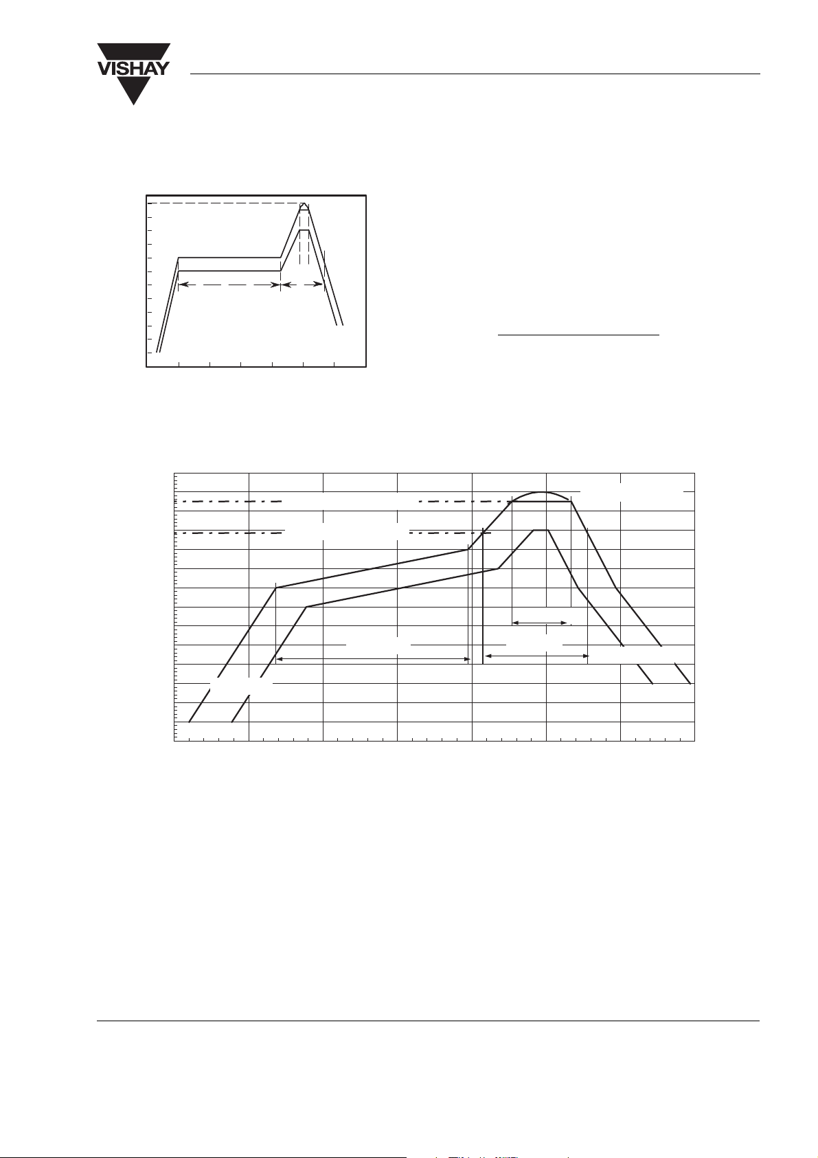
Recommended Solder Profile
Solder Profile for Sn/Pb soldering
240
220
14874
200
180
160
140
120
100
80
60
Temperature (°C)
40
20
0
2°C-4°C/s
0 50 100 150 200 250 300 350
Figure 2. Recommended Solder Profile
280
260
240
220
200
180
160
140
120
Temperature/° C
100
80
60
40
20
0
0 50 100 150 200 250 300 350
2°C-4°C/s
90 s max120 s - 180 s
Time(s)
T = 250°C for 10 s....40 s
T = 217°C for 70 s max
2°C...3°C/s
10 s max.
@ 230 °C
90 s...120 s
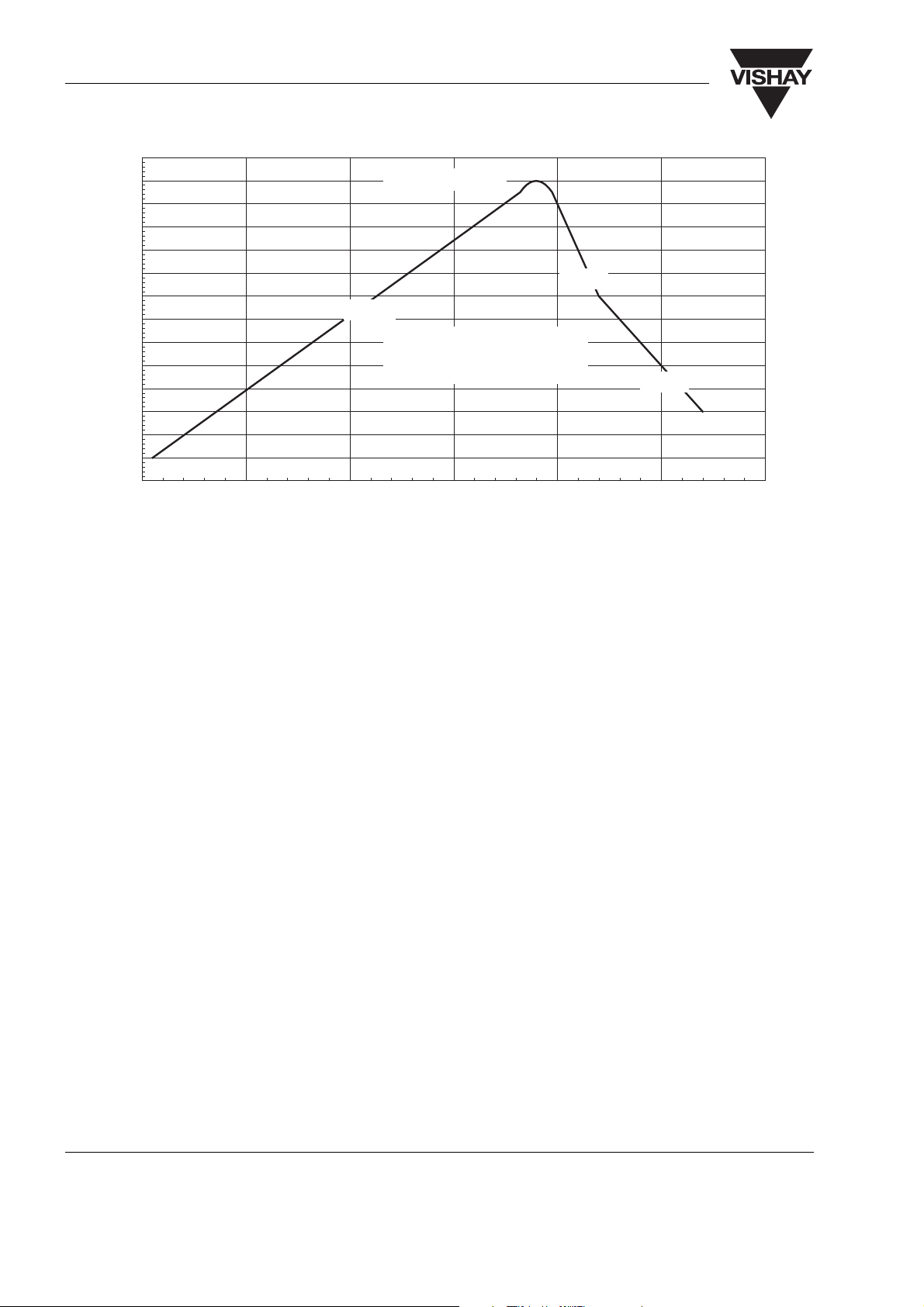
Lead-Free, Recommended Solder Profile
This device is a lead-free transceiver and qualified for
lead-free processing. For lead-free solder paste like
Sn
(3.0 - 4.0)Ag(0.5 - 0.9)
reflow profiles: Ramp-Soak-Spike (RSS) and RampTo-Spike (RTS). The Ramp-Soak-Spike profile was
developed primarily for reflow ovens heated by infrared radiation. With widespread use of forced convection reflow ovens the Ramp-To-Spike profile is used
increasingly. Shown below in figure 3 and figure 4 are
Vishay’s recommended profile for use with this transceiver type. For more details please refer to Application note: SMD Assembly Instruction
40 s max.
70 s max.
Time/s
Cu, there are two standard
.
T
= 260°C max.
peak
2°C...4°C/s
Document Number 82558
Rev. 1.6, 12-Aug-04
Figure 3. Solder Profile, RSS Recommendation
www.vishay.com
9
Page 10
TFDU8108
Vishay Semiconductors
280
260
240
220
200
180
160
140
120
Temperature/°C
100
80
60
40
20
0
0 50 100 150 200 250 300
T
= 260°C max.
peak
1.3°C/s
Time above 217°C t ≤ 70 s
Time above 250°C t ≤ 40 s
Peak temperature T
Time/s
peak
<4°C/s
= 260°C
<2°C/s
Figure 4. Solder Profile, RTS Recommendation
A ramp-up rate smaller than 0.9 °C/s is not recommended. Ramp-up rates faster than 1.3 °C/s could
damage an optical part because the thermal conductivity is less than compared to a standard IC.
www.vishay.com
10
Document Number 82558
Rev. 1.6, 12-Aug-04
Page 11

Current Derating Diagram
600
500
400
300
Current derating as a function of
200
the maximum forward current of
IRED. Maximum duty cycle: 25%.
100
Peak Operating Current ( mA )
0
–40 –20 0 20 40 60 80 100 120 140
14875
Temperature ( °C )
Figure 5. Current Derating Diagram
TFDU8108
Vishay Semiconductors
Document Number 82558
Rev. 1.6, 12-Aug-04
www.vishay.com
11
Page 12
TFDU8108
Vishay Semiconductors
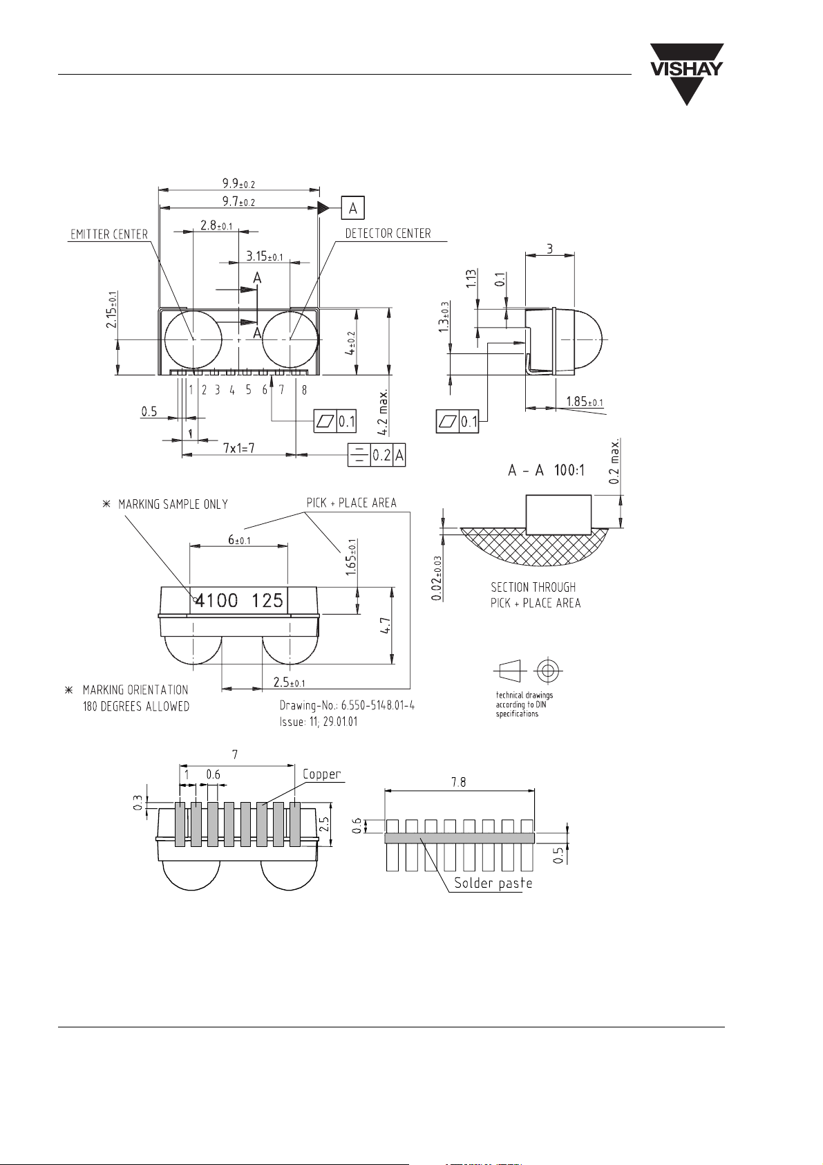
Package Dimensions in mm
www.vishay.com
12
Document Number 82558
Rev. 1.6, 12-Aug-04
Page 13

Appendix A
Serial Interface Implementation
Basics of the IrDA Definitions
17092
Figure 6. Interface to Two Infrared Transceivers
TFDU8108
Vishay Semiconductors
The data lines are multiplexed with the transmitter
and receiver signals and separate clocks are used
since the transceivers respond to the same address.
17093
Figure 7. Infrared Dongle with Differential Signaling
When no infrared communication is in progress and
the serial bus is idle, the IRTX line is kept low and
IRRX is kept high.
Document Number 82558
Rev. 1.6, 12-Aug-04
www.vishay.com
13
Page 14

TFDU8108
Vishay Semiconductors
Functional description
The serial interface is designed to interconnect two or
more devices. One of the devices is always in control
of the serial interface and is responsible for starting
every transaction. This device functions as the bus
master and is always the infrared controller. The infrared transceivers act as bus slaves and only respond
to transactions initiated by the master. A bus transaction is made up of one or two phases. The first phase
is the Command Phase and is present in every transaction. The second phase is the Response Phase
and is present only in those transactions in which data
must be returned from the slave. If the operation
involves a data transfer from the slave, there will be a
Response Phase following the Command Phase in
which the slave will output the data.
The Response Phase, if present, must begin 4 clock
cycles after the last bit of the Command Phase, as
shown in figures 1 - 7 and 1 - 8, otherwise it is
assumed that there will be no response phase and the
master can terminate the transaction.
The SCLK line is always driven by the master and is
used to clock the data being written to or read from
the slave.
This line is driven by a totem-pole output buffer. The
SCLK line is always stopped when the serial interface
is idle to minimize power consumption and to avoid
any interference with the analog circuitry inside the
slave. There are no gaps between the bytes in either
the Command or Response Phase. Data is always
transferred in Little Endian order (least significant bit
first). Input data is sampled on the rising edge of
SCLK. IRTX/SWDAT output data from the controller
is clocked by SCLK falling edge. IRRX/SRDAT output
data from the slave is clocked by SCLK rising edge.
Each byte of data in both Command and Response
Phases is preceded by one start bit. The data to be
written to the slave is carried on the IRTX/SWDAT
line. When the control interface is idle, this line carries
the infrared data signal used to drive the transmitter
LED. When the first low-to-high transition on SCLK is
detected at the beginning of the command sequence,
the slave will disable the transmitter LED. The infrared
controller then outputs the command string on the
IRTX/SWDAT line. On the last SCLK cycle of the
command sequence the slave re-enables the transmitter LED and normal infrared transmission can
resume. No transition on SCLK must occur until the
next command sequence otherwise the slave will disable the transmitter LED again. Read data is carried
on the IRRX/SRDAT line. The slave disables the
internal signal from the receiver photo diode during
the response phase of a read transaction. The
addressed slave will output the read data on the
IRRX/SRDAT line regardless of the setting of the
Receiver Output Enable bit in the Mode Selection register 0. Non addressed slaves will tri-state the IRRX/
SRDAT line. When the transceiver is powered up, the
IRTX/SWDAT line should be kept low and SCLK
should be cycled at least 30 times by the infrared controller before the first command is issued on the IRTX/
SWDAT line. This guarantees that the transceiver
interface circuitry will properly initialize and be ready
to receive commands from the controller. In case of a
multiple transceiver configuration, only one transceiver should have the receiver output enabled. A
series resistor (approx. 200 ohms) should be placed
on the receiver output from each transceiver to prevent large currents in case a conflict occurs due to a
programming error.
SCLK
IRTX/
SWDAT
IRRX/
SRDAT
TLED_DIS
(INTERNAL SIGNAL)
17175
Figure 8. Initial Reset Timing
SCLK
IRTX/
SWDAT
IRRX/
(Note 1)
SRDAT
TLED_DIS
(INTERNAL SIGNAL)
RES
(INTERNAL SIGNAL)
17176
Figure 9. Special Command Waveform
www.vishay.com
14
Document Number 82558
Rev. 1.6, 12-Aug-04
Page 15

TFDU8108
Vishay Semiconductors
17177
Figure 10. Write Data Waveform
Note 1: If the APEN bit in control register 0 is set to 1, the internal
signal from the receiver photo diode is discon nected and the IRRX/
SRDAT line is pulsed low for one clock cycle at the end of a write
or special command.
17178
Figure 11. Write Data Waveform with Extended Index
17179
Figure 12. Read Data Waveform
17180
Figure 13. Read Data Waveform with Extended Index
Note 2: During a read transaction the infrared controller sets the
IRTX/SWDAT line high after sending the address and index byte
(or bytes). It will then set it low two clock cycles before the end of
the transaction. It is strongly recommended that optical transceiv-
ers monitor this line instead of counting clock cycles in order to
detect the end of the read trans action. This will always guarantee
correct operation in case two or more transceivers from different
manufacturers are sharing the serial interface.
Document Number 82558
Rev. 1.6, 12-Aug-04
www.vishay.com
15
Page 16

TFDU8108
Vishay Semiconductors
Switching Characteristics
Maximum capacitive load = 20 pF
Parameters Test Conditions Symbol Min. Max. Unit
SCLK Clock Period R.E., SCLK to next R.E., SCLK tCKp 250 infinity ns
SCLK Clock High Time At 2.0 V for single-ended signals tCKh 60 ns
SCLK Clock Low Time At 0.8 V for single-ended signals tCKl 80 ns
Output Data Valid
(from infrared controller)
Output Data Hold
(from infrared controller)
Output Data Valid
(from optical transceiver)
Output Data Hold
(from optical transceiver)
Line Float Delay After R.E., SCLK tDOrf 60 ns
Input Data Setup Before R.E., SCLK tDIs 10 ns
Input Data Hold After R.E., SCLK tDIh 5 ns
*)
Capacitive load is different from "Serial interface - specification". For the bus protocol see "RECOMMENDED SERIAL INTERFACE FOR
TRANSCEIVER CONTROL, Draft Version 1.0a, March 29, 2000, IrDA". In Appendix B the transceiver related data are given.
*)
After F.E., SCLK tDOtv 40 ns
After F.E., SCLK tDOth 0 ns
After R.E., SCLK tDOrv 40 ns
After R.E., SCLK tDOrh 40 ns
www.vishay.com
16
Document Number 82558
Rev. 1.6, 12-Aug-04
Page 17

TFDU8108
Vishay Semiconductors
Appendix B
Application Guideline
In the following some guideline is given for handling
the TFDU8108 in an application ambient, especially
for testing. It is also a guideline for interfacing with a
controller. We recommend to use for first evaluation
the Vishay IRM1802 controller. For more information
see the special data sheet. Driver software is available on request. Contact irdc@vishay.com.
Serial Interface Capability of the Vishay
IrDA Transceivers
Abstract
A serial interface allows an infrared controller to communicate with one or more infrared transceivers. The
basic specification of IrDA) specified interface is
described in "Serial Interface for Transceiver Control,
v 1.0a", IrDA.
This part of the document describes the capabilities of
the serial interface implemented in the Vishay IrDA
transceivers TFDU8108 and TFDU6108. The VFIR
(16 Mbit/s) and FIR (4 Mbit/s) programmable versions
are using the same interface specification. (with specific identification and programming).
IrDA Serial Interface Basics
The serial interface for transceiver control (SITC) is a
master/slave synchronous serial bus which uses the
Txd and Rxd as data lines and the SCLK as clock line
with a minimum period of 250 ns. The transceiver
works always as slave and jump into SITC mode on
the first rising edge of the clock line remaining there
until the command phase is finished. After power on it
is required an initial phase for ≥ 30 clock cycles at Txd
is continuous low before the transmitter can be programmed. If Txd assume high during the initial phase
then must start the initial phase again.
The data transfer is organized by one byte preceded
by one start bit. The SITC allows the communication
between infrared controller and transceiver through
write and read transaction. The SITC consists of two
store blocks with different functions. The store block
called Extended Indexed Registers contain the various supported functionality of the device and can be
read only. The other Main Control Registers allow
write and read transaction and store the executable
configuration of the device.
Any configuration is executed after the command
phase is completed.
Power-on
After power on the transceiver is to stay by definition in the default mode shown in the table.
Function TFDU8108
Power Mode sleep
RX disable (Z)
TX_LED: disable
APEN disable
Infrared Mode SIR
Transmitter Power max. SIR power level
Addressing
The transceiver is addressable with three address bits. There are individual and common addresses with the following values.
Description Address value A [2:0]
Individual address Mask programmable 010
Common (broadcast) address 111
Data Acknowledgement
Data acknowledgement generated by the slave is
available if the APEN bit is set to 1 in the common
control register. In IrDA default state this functionality
is disabled. In default state of the TFDU8108 it is
enabled (see above). It is strongly recommended that
this functionality is enabled to be on the safe side for
correct data transmission during SITC mode.
Document Number 82558
Rev. 1.6, 12-Aug-04
www.vishay.com
17
Page 18

TFDU8108
Vishay Semiconductors
Registers Data Depth
In general the whole data registers consist of a data
depth of eight bits. But sometimes it is unnecessary to
implement the full depth. In such a case the invisible
bits consider like a zero.
Used Index Commands
The table shows the valid index commands, its allowable modes, and the data depth to them.
Commands INDEX
[3:0]
0h W/R Common control main-ctrl-0 register [4:0] 00h
1h W/R Infrared mode main-ctrl-1 register [7:0] 00h
2h W/R Txd power level main-ctrl-2 register [7:4] 70h
Bh - 3h X Not used
Ch X Not used
Dh W Reset transceiver,
Eh X Not used
Fh W Not used
Note: The main_ctrl_1 register is written software dependent on the offset value stored in ext_ctrl_7 and ext_ctrl_8 registers.
The main_ctrl_1 register can be set to the following values, shown in the table.
Mode Actions Register Name Data Bits TFDU8108
default
Only one byte!
R Not used
R Extended indexing
Main-ctrl-0 register values
Valu e Function Default
bit 0 PM SL - Power Mode Select
0 > low power mode (sleep mode)
1 > normal operation power mode
bit 1 RX OEN - Receiver Output Enable
bit 2 TLED EN - Transmitter LED Enable
bit 3 not used not used
bit 4
1)
APEN - Acknowledge Pulse Enable, (optional)
This bit is used to enable the acknowledge pulse. When it is set to 1 and RX OEN is 1 (receiver output enabled) the IRRX/SRDAT line will
be pulsed low for one clock cycle upon successful completion of every write command or special command with individual (non broadcast)
transceiver address. The internal signal from the receiver photo diode is disconnected when this bit is set to 1.
0 > IRRX/SRDAT line disable (tri-stated)
1 > IRRX/SRDAT line enabled
0 > disabled
1 > enabled
1)
APEN
sleep
disable
disable
disable
www.vishay.com
18
Document Number 82558
Rev. 1.6, 12-Aug-04
Page 19

TFDU8108
Vishay Semiconductors
Main-ctrl-1 register values
Val ue Funtion
00h SIR (default)
01h MIR
02h FIR
03h
05h VFIR - 16
08h
Depending on the values of "ext_ctrl_7" and "ext_ctrl_8" it must be checked if the value for main_ctrl_1 is correct. If it cause an error then
the transceiver will load 00h into the main_ctrl_1 register and will not give an acknowledgement.
Apple Talk
Sharp IR
Main-ctrl-2 register values
bit 7 bit 6 bit 5 bit 4 bit 3 bit 2 bit 1 bit 0 Mode Txd - IRED
8xh-
Fxh
7xh
6xh 0 1 1 0 SIR > 0.7 m
5xh 0 1 0 1 SIR > 0.5 m
4xh 0 1 0 0 (45)
3xh 0 0 1 1 SIR > 0.35 m
2xh 0 0 1 0 SIR > 0.25 m
1xh 0 0 0 1 SIR > 0.15 m
0xh0000xxxx 0
1)
IrDA default setting
1xxxxxxx VFIR > 1 m,
1)
0111xxxx SIR >1 m
®
(FIR functionality)
®
(SIR functionality)
FIR > 1 m
not for SIR!
FIR > 0.7 m
VFIR > 0.7 m
FIR > 0.45 m
VFIR > 0.45 m
FIR > 0.3 m
VFIR > 0.3 m
FIR > 0.2 m
VFIR > 0.2 m
FIR > 0.15 m
VFIR > 0.2 m
FIR > 0.1 m
VFIR > 0.1 m
[mA]
550
(switch, ext.
R1!)
250 SIR, More Ext.
125 Extended VFIR/FIR
60 VFIR/FIR Low Power
30 SIR Low Power
15 e.g. Docking station
8 e.g. Docking station
Remark
VFIR/FIR standard,
serial resistor is
necessary for
V
> 4 V
CC2
VFIR/FIR LP
Low Power
Document Number 82558
Rev. 1.6, 12-Aug-04
www.vishay.com
19
Page 20

TFDU8108
Vishay Semiconductors
Used Extended Indexed Registers
The table shows the valid extended indexed commands its allowable modes and the data depth to them.
Register
Address
E_INDEX [7:0]
00h R Manufactured ID Ext_Ctrl_0 [7:0] 0:4h
01h R Device ID Ext_Ctrl_1 [7:0] [7:6] <- 11
04h R Receiver recovery time
05h R Receiver stabilization
06h R Common capabilities Ext_Ctrl_6 [7:0] 03h
07h R Supported Infrared modes Ext_Ctrl_7 [7:0] 0Fh
08h R Supported Infrared modes Ext_Ctrl_8 0 01h
09h - FFh
except F0h
F0h R Chip specific register Ext_Ctrl_240 [7:0] Not disclosed
Mode Action Register Name Data Bits Fixed Value
Ext_Ctrl_4 [6:4, 2:0] 24h
Power on stabilization
Ext_Ctrl_5 [6:4, 2:0] 30h
SCLK max. frequency
X Not used
(See 1.1.7)
[5:3] <- xxx
[2:0] <- xxx
xxx: Version
number
Invalid Commands Handling
There are some commands and register addresses, which cannot be decoded by the SITC. The slave ignores such invalid data for the
internal logic. Below the different types and the slave reaction to them are shown.
Description Master Command Slave Reaction on IRRX/SRDAT
Invalid command in read mode Index [3:0] & C = 0 no reaction
Invalid command in write mode Index [3:0] & C = 1 No acknowledgement generating
Valid command in invalid read mode Index [3:0] & C = 0 no reaction
Valid command in invalid write mode Index [3:0] & C = 1 No acknowledgement generating
Valid command in invalid write mode and
invalid data
Broadcast address in read mode A [2:0] = 111 & C = 0 no reaction
No reaction means that the slave does not start the respond phase.
Index [3:0] & C = 1 No acknowledgement generating
independent of the value of APEN
independent of the value of APEN
independent of the value of APEN
Reset
There is no external reset pin at Vishay IrDA transceivers. In case of transition error there are two ways
to set the SITC in a defined state: The first one is
power off. The second one is that the transceiver
monitors the IRTX/SWDAT line in any state. If this line
is assumed low for ≥ 30 clock cycles then the trans-
ceiver must be set to the command start state and set
all registers to default implemented values.
www.vishay.com
20
Document Number 82558
Rev. 1.6, 12-Aug-04
Page 21

Appendix C
TFDU8108
Vishay Semiconductors
Serial Interface (SIF) Programming Guide
The SIF port of this module allow an IR controller to
communicate with it, get module ID and capability
information, implement receiver bandwidth mode
switching, LED power control, shutdown and some
other functions.
This interface requires three signals: a clock line
(SCLK) that is used for timing, and two unidirectional
lines multiplexed with the transmitter (Txd, write) and
receiver (Rxd, read) infrared signal lines.
The supported programming sequence formats are
listed below:
one-byte special commands
two-byte write commands
two-byte read commands
three-byte read commands
The one-byte special command sequences are
reserved for time-critical actions, while the two-byte
write command is predominantly used to set basic
transceiver characteristics. More information can be
found in the IrDA document "Serial Interface for
Transceiver Control, v 1.0a" on IrDA.org web site.
Serial Interface Timing Specifications
In general, serial interface programming sequences
are similar to any clocked-data protocol:
• there is a range of acceptable clock rates, measured from rising edge to rising edge
• there is a minimum data setup time before clock rising edges
• there is a minimum data hold time after clock rising
edges
Recommended programming timing:
(4 kHz <) fclk < 8 MHz (4 kHz is a recommended
value, according to the Serial Interface Standard
quasi-static programming is possible)
TCLK > 125 ns (< 250 µs, see the remark for quasistatic programming above)
Tsetup > 10 ns
Thold > 10 ns
The timing diagrams below show the setup and hold
time for Serial Interface programming sequences:
SCLK
TX
Tsetup > 10 ns
Thold > 10 ns
18496
125 ns < Tclk
s
Protocol Specifications
The serial interface protocol is a command-based
communication standard and allows for the communication between controller and transceiver by way of
serial programming sequences on the clock (SCLK),
transmit (TX), and receive (RX) lines. The SCLK line
is used as a clocking signal and the transmit/receive
lines are used to write/read data information. The protocol requires all transceivers to implement the write
commands, but does not require the read-portion of
the protocol to be implemented (though all transceivers must at least follow the various commands, even
if they perform no internal action as a result). This
serial interface follows but does not support all read/
write commands or extended commands, supporting
only the special commands and basic write/read commands.
Write commands to the transceiver take place on the
SCLK and TX lines and may make use of the RX line
for answer back purposes.
A command may be directed to a single transceiver
on the SCLK, TX and RX bus by specifying a unique
three-bit transceiver address, or a command may be
directed to all transceivers on the bus by way of a special three-bit broadcast address code. The Vishay
VFIR transceiver TFDU8108 will respond to transceiver address 010 and the broadcast address 111
only, and follows but ignores all other transceiver
addresses. The transceiver address of Vishay FIR
module TFDU6108 is 001.
All commands have a common \"header\" or series of
leading bits which take the form shown below.
first bit sent to
transceiver
0 1 1/0 R0 R1 R2 R3 A0 A1 A2
last bit sent to
transceiver
...
Document Number 82558
Rev. 1.6, 12-Aug-04
Sync
Bits
1=Write
0=Read
Register
Address
or Code
Transceiver
Address
18497
www.vishay.com
21
Page 22
TFDU8108
Vishay Semiconductors
The bits shown are placed on the TX (DATA) line and
clocked into the transceiver using the rising edge of
the SCLK signal. Only the data bits are shown as it is
assumed that a clock is always present, and that the
transceiver samples the data on the rising edge of
each clock pulse.
Note: as illustrated in the diagram above, the protocol
uses "Little Endian" ordering of bits, so that the LSB is
sent first, and the MSB is sent last for register
addresses, transceiver addresses, and read/write
data bytes. The notation that follows presents all
addresses and data in LSB-to-MSB order (bits 0, 1, 2,
3, ... 7) unless otherwise stated.
Command Module Type Programming Sequence
RESET
(Set all registers to default value)
TFDU6108 011 1011 100 00 3B
TFDU8108 011 1011 010 00 5B
One-byte Special Commands
One-byte special commands are used for time-critical
transceiver commands, such as full transceiver reset.
A total of six special commands are possible,
although only one command is available on the
TFDU8108 and TFDU6108.
0 1 1 R0 R1 R2 R3 A0 A1 A2
18498
Sync
Bits
Write
(Binary)
Special
Command
Code
Transceiver
Address
Programming Sequence
00
Stop
Bits
(Hex)
Two-byte Write Commands
Two-byte write commands are used for setting the
contents of transceiver registers which control transceiver such as shutdown/enable, receiver mode, LED
power level, etc.
The register space requires four register address bits
(R0-3), although three codes are used for controlling
transceiver (see above), and the 1111 escape code is
for extended commands. The 3-bit transceiver
address (A0-3) is for selecting the destination, e.g.
010 to TFDU8108 and 001 to TFDU6108.
The second byte is data field (D0-7) for setting the
characteristics of the transceiver module, e.g. SIR
mode (00) or VFIR (05) when the register address is
0001.
The basic two-byte write command is illustrated
below:
0 1 1 R0 R1 R2 R3 A0 A1 A2
Sync
18499
Bits
Write
Register
Address
Transceiver
Address
1 D0..D7
8-D at a
Bits
00
Stop
Bits
www.vishay.com
22
Document Number 82558
Rev. 1.6, 12-Aug-04
Page 23

Some important serial interface programming
sequences are shown below:
TFDU8108
Vishay Semiconductors
Command TFDU6108 Programming Sequence
(Transceiver address: 001)
Common Ctrl (0000) Value (hex)
Normal (Enable all) 0F 011 0000 100 1 11110000 00 011 0000 010 1 11110000 00
Shutdown 00 011 0000 100 1 00000000 00 011 0000 010 1 00000000 00
Receiver Mode (0001) Value (hex)
SIR 00 011 1000 100 1 00000000 00 011 1000 010 1 00000000 00
MIR 01 011 1000 100 1 10000000 00 011 1000 010 1 10000000 00
FIR 02 011 1000 100 1 01000000 00 011 1000 010 1 01000000 00
Apple Talk 03 011 1000 100 1 11000000 00 011 1000 010 1 11000000 00
VFIR 05 011 1000 100 1 10100000 00 011 1000 010 1 10100000 00
Sharp-IR 08 011 1000 100 1 00010000 00 011 1000 010 1 00010000 00
LED Power (0010) Value (hex)
8 mA 1X 011 0100 100 1 00001000 00 011 0100 010 1 00001000 00
15 mA 2X 011 0100 100 1 00000100 00 011 0100 010 1 00000100 00
30 mA 3X 011 0100 100 1 00001100 00 011 0100 010 1 00001100 00
60 mA 5X 011 0100 100 1 00001010 00 011 0100 010 1 00001010 00
125 mA 6X 011 0100 100 1 00000110 00 011 0100 010 1 00000110 00
250 mA 7X 011 0100 100 1 00001110 00 011 0100 010 1 00001110 00
500 mA FX 011 0100 100 1 00001111 00 011 0100 010 1 00001111 00
TFDU8108 Programming Sequence
(Transceiver address: 010)
Document Number 82558
Rev. 1.6, 12-Aug-04
www.vishay.com
23
Page 24

TFDU8108
Vishay Semiconductors
Reel Dimensions
W
1
Reel Hub
W
2
Tape Width A max. N W1 min. W2 max. W3 min. W3 max.
mm mm mm mm mm mm mm
24 330 60 24.4 30.4 23.9 27.4
14017
www.vishay.com
24
Document Number 82558
Rev. 1.6, 12-Aug-04
Page 25

Tape Dimensions in mm
TFDU8108
Vishay Semiconductors
Document Number 82558
Rev. 1.6, 12-Aug-04
18269
www.vishay.com
25
Page 26

TFDU8108
Vishay Semiconductors
www.vishay.com
26
18283
Document Number 82558
Rev. 1.6, 12-Aug-04
Page 27

TFDU8108
Vishay Semiconductors
Ozone Depleting Substances Policy Statement
It is the policy of Vishay Semiconductor GmbH to
1. Meet all present and future national and international statutory requirements.
2. Regularly and continuously improve the performance of our products, processes, distribution and
operatingsystems with respect to their impact on the health and safety of our employees and the public, as
well as their impact on the environment.
It is particular concern to control or eliminate releases of those substances into the atmosphere which are
known as ozone depleting substances (ODSs).
The Montreal Protocol (1987) and its London Amendments (1990) intend to severely restrict the use of ODSs
and forbid their use within the next ten years. Various national and international initiatives are pressing for an
earlier ban on these substances.
Vishay Semiconductor GmbH has been able to use its policy of continuous improvements to eliminate the use
of ODSs listed in the following documents.
1. Annex A, B and list of transitional substances of the Montreal Protocol and the London Amendments
respectively
2. Class I and II ozone depleting substances in the Clean Air Act Amendments of 1990 by the Environmental
Protection Agency (EPA) in the USA
3. Council Decision 88/540/EEC and 91/690/EEC Annex A, B and C (transitional substances) respectively.
Vishay Semiconductor GmbH can certify that our semiconductors are not manufactured with ozone depleting
substances and do not contain such substances.
We reserve the right to make changes to improve technical design
and may do so without further notice.
Parameters can vary in different applications. All operating parameters must be validated for each
customer application by the customer. Should the buyer use Vishay Semiconductors products for any
unintended or unauthorized application, the buyer shall indemnify Vishay Semiconductors against all
claims, costs, damages, and expenses, arising out of, directly or indirectly, any claim of personal
damage, injury or death associated with such unintended or unauthorized use.
Vishay Semiconductor GmbH, P.O.B. 3535, D-74025 Heilbronn, Germany
Telephone: 49 (0)7131 67 2831, Fax number: 49 (0)7131 67 2423
Document Number 82558
Rev. 1.6, 12-Aug-04
www.vishay.com
27
 Loading...