

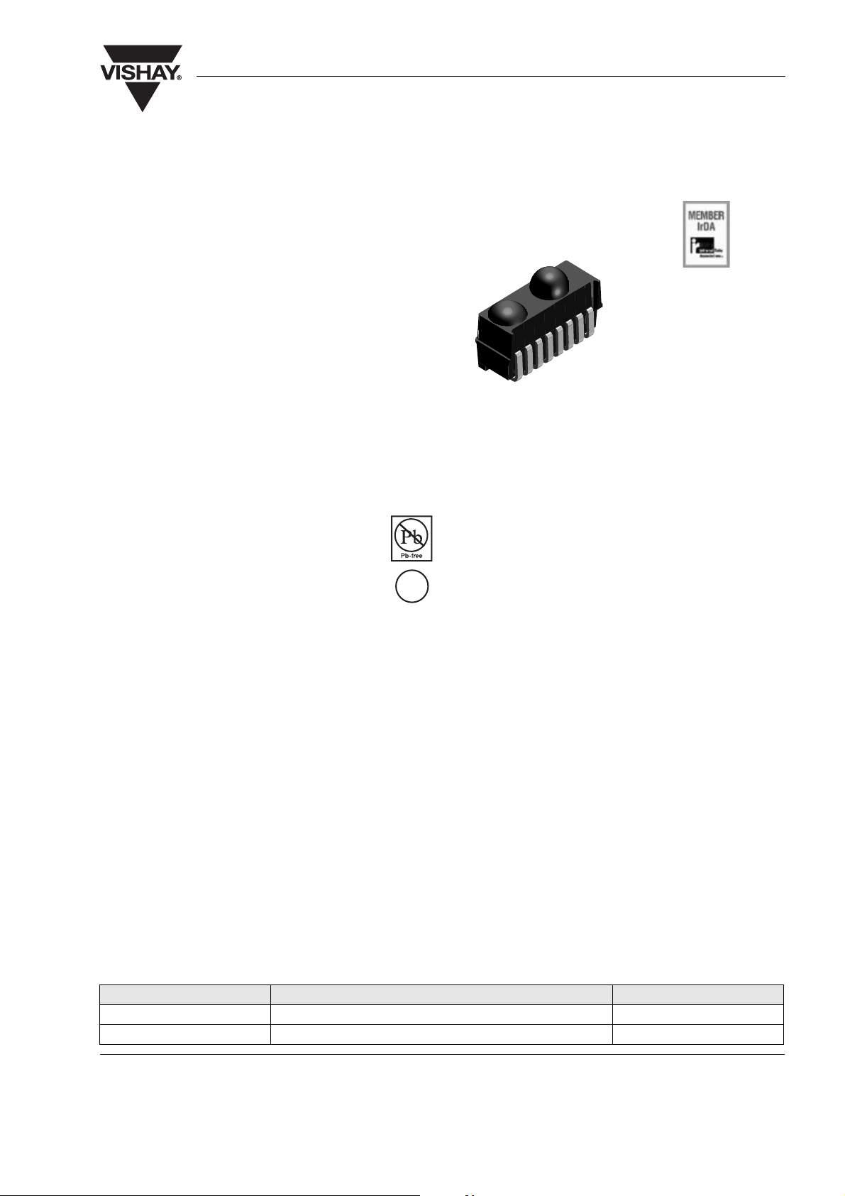
TFDU4202
Vishay Semiconductors
Integrated Low Profile Transceiver Module for Telecom
Applications - IrDA Standard
Description
The miniaturized TFDU4202 is an ideal transceiver
for applications in telecommunications like mobile
phones and pagers. The device is mechanically
designed for lowest profile with a height of only
2.8 mm. The infrared transceiver is compatible to the
latest IrDA
115 kbit/s. At lower operating voltages up to 3.3 V the
transceiver can be operated without external current
limiting resistor to achieve a range > 1 m.
The added feature is a split power supply for IRED
driver (V
For operating only in the limited distance, low power
range (20 cm/ 30 cm), TFDU4201 with built-in current
control is recommended. For this device see the
appropriate data sheet.
®
IrPHY specification up to a data rate of
) and ASIC (V
ccp
ccp
).
18170
Features
• Package dimension microFace
TFDU4202:
L 7.1 mm x W 4.7 mm x H 2.8 mm
• Compatible to latest IrDA IrPHY standard
• CIR Remote Control operation:
Typical transmission range 8 m using standard
RC-receivers. Receives RC-commands with
typical specified sensitivity.
• SMD Side View
• Lowest power consumption 65 µA, receive mode,
0.01 µA Shutdown
• Built-in current limitation
• Output intensity adjustable by external resistor
• Wide supply voltage range (2.4 V to 5.5 V)
• Split power supply
e3
Applications
• Mobile Phones
• Pagers
• Personal Digital Assistants (PDA)
• Handheld Battery Operated Equipment
• Operational down to 2.0 V
• Fewest external components
• Eye safety: Double safety
Measures:
Limited optical output oulse duration
Limited optical output intensity
IEC60825-1, 2001: Class 1
• Push-pull output (RXD)
• High EMI immunity
• Split power supply, transmitter and receiver can be
operated from two power supplies with relaxed
requirements saving costs, US Patent No.
6,157,476
• Lead (Pb)-free device
• Device in accordance to RoHS 2002/95/EC and
WEEE 2002/96/EC
Parts Table
Par t Description Qty / Reel
TFDU4202-TR1 Orientated in carrier tape for side view in mounting 750 pcs
TFDU4202-TR3 Orientated in carrier tape for side view in mounting 2250 pcs
Document Number 82541
Rev. 1.8, 05-Dec-05
www.vishay.com
1
TFDU4202
Vishay Semiconductors
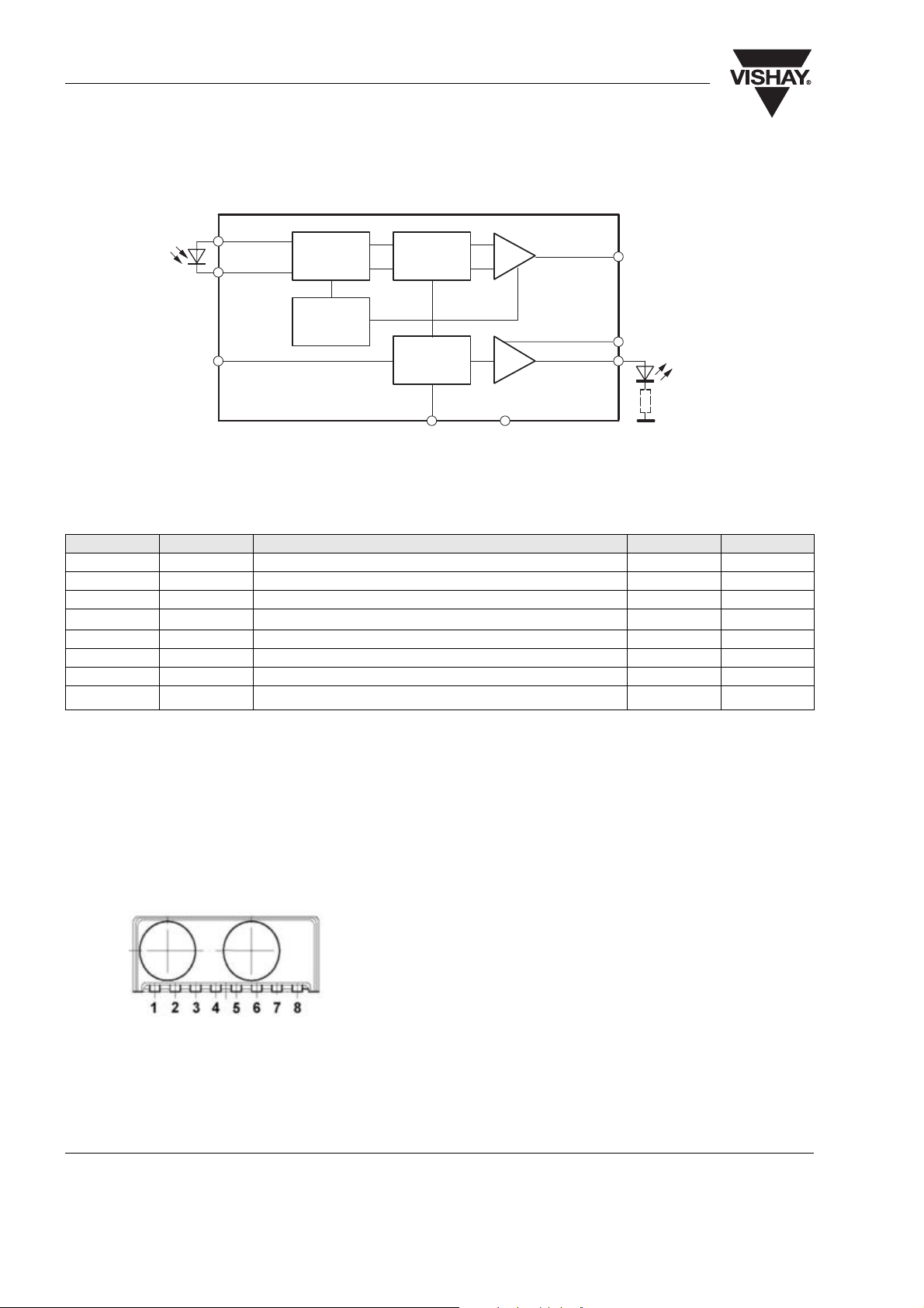
Functional Block Diagram
TXD
Amplifier
Control
Logic
Comparator
Control
Tri-State-Driver
Controlled Driver
RXD
V
ccp
18190
V
CC
GND
Pin Description
Pin Number Function Description I/O Active
1 IRED GND IRED cathode, ground
2 IRED GND IRED cathode, ground
3 RXD Output, received data, push-pull output O low
4V
5 GND Ground
6 GND Ground
7 TXD Input, transmit data I high
8
*)
VCC is allowed to be switched off for standby with V
CCP
*)
V
CC
IRED supply voltage
Power supply voltage I high
applied.
ccp
Pinout
TFDU4202
weight 100 mg
18228
www.vishay.com
2
Document Number 82541
Rev. 1.8, 05-Dec-05
TFDU4202
Vishay Semiconductors
Absolute Maximum Ratings
Reference Point Pin 8, unless otherwise noted.
Parameter Test Conditions Symbol Min Ty p. Max Unit
Supply voltage range V
CC
V
ccp
Input current all pins 10 mA
Output sink current 25 mA
Power dissipation P
Junction temperature T
Ambient temperature range
tot
J
T
amb
(operating)
Storage temperature range T
stg
Soldering temperature see the chapter “Soldering
conditions” for lead-bearing and
Pb-free processing
Average IRED current I
Repetitive pulsed IRED current < 90µs, t
< 20 % I
on
Transmitter data input voltage V
Receiver data output voltage V
IRED(DC)
IRED(RP)
TXD
RXD
- 0.5 6 V
- 0.5 6 V
200 mW
125 °C
- 25 85 °C
- 40 100 °C
260 °C
125 mA
500 mA
- 0.5 6 V
- 0.5 6 V
Eye safety information
Parameter Test Conditions Symbol Min Ty p. Max Unit
Virtual source size Method: (1 - 1/e) encircled
d2mm
energy
Compatible to Class 1 operation of IEC 60825 or EN60825 with worst case IrDA SIR pulse pattern, 115.2 kbit/s
Electrical Characteristics
Transceiver
Tested for the following parameters (VCC = 2.4 V to 5.5 V, - 25 °C to + 85 °C, unless otherwise stated).
Parameter Test Conditions Symbol Min Ty p. Max Unit
Supported data rates base band 9.6 115.2 kbit/s
Supply voltage range operational down to 2.0 V V
Supply current V
= 2.4 V to 5.5 V, Ee = 0,
CC
receive mode, full temperature
range
= 2.4 V to 5.5 V, 10 klx
V
CC
sunlight, receive mode, full
temperature range, no signal
V
CC
= 2.7 V, V
= 2.7 V,
ccp
115.2 kbit/s transmission,
receive mode,
nose to nose operation
Supply current at V
ccp
shutdown mode, entire
temperature range 20 °C
= 0 V, entire temperature
V
CC
I
Sshdown
I
Sshdown
range 20 °C
IRED peak current transmitting I
= 40 mW/sr, no external
e
resistor V
= 2.7 V, SIR
ccp
standard
Transceiver ‘power on‘ settling
time
time from switching on V
CC
to
established specified operation
CC
I
S
I
S
I
S
I
Str
2.4 5.5 V
65 100 µA
70 100 µA
1mA
0.02 1 µA
10 nA
360 mA
1ms
Document Number 82541
Rev. 1.8, 05-Dec-05
www.vishay.com
3
TFDU4202
Vishay Semiconductors
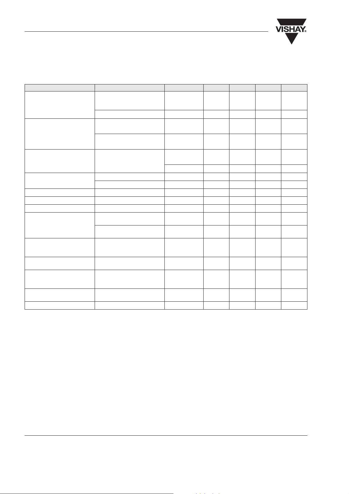
Optoelectronic Characteristics
Receiver
Tested for the following parameters (VCC = 2.4 V to 5.5 V, - 25 °C to + 85 °C, unless otherwise stated).
Parameter Test Conditions Symbol Min Ty p . Max Unit
Minimum detection threshold
irradiance (logic high receiver
| α | ≤ ± 15 °,
V
= 2.4 V to 5.5 V
CC
input irradiance)
2.0 V, 25 °C tested E
Maximum detection threshold
| α | ≤ ± 90 °, VCC = 5 V E
irradiance
| α | ≤ ± 90 °, V
= 3 V E
CC
Logic low receiver input
irradiance
Output voltage RXD active, C = 15 pF V
non active, C = 15 pF V
Output current RXD V
< 0.5 V 4 mA
OL
Rise time at load C = 15 pF, R = 2.2 kΩ t
Fall time at load C = 15 pF, R = 2.2 kΩ t
RXD signal electrical output
pulse width
2.4 kbit/s, input pulse width
1.41 µs to 3/16 of bit duration
115.2 kbit/s, input pulse width
1.41 µs to 3/16 of bit duration
Output delay time (RXD),
leading edge optical input to
electrical output
Jitter, leading edge of output
signal
Output delay time (RXD), trailing
edge optical input to electrical
output
output level =
0.5 x V
@ 40 mW/m
CC
over a period of 10 bit,
115.2 kbit/s
output level =
0.5 x V
@ 40 mW/m
CC
2
2
Power on time, SD recovery
time
Latency t
E
e, min
e, min
e, max
e, max
E
e, max,low
E
e, max,low
OL
OH
t
t
t
dl
t
t
dt
3300
(330)
8000
(800)
00.5V
VCC - 0.5 V
r
f
p
p
j
L
20 70 ns
20 70 ns
1.41 20 µs
1.41 4.5 µs
25
(2.5)
50 100
5000
(500)
15000
(1500)
50
(5)
4
(0.4)
mW/m
(µW/cm
mW/m
W/m
(mW/cm
W/m
(mW/cm
mW/m
(µW/cm
µW/m
2
2
)
2
2
2
)
2
2
)
2
2
)
2
12µs
400 ns
6.5 µs
0.1 1 ms
100 200 µs
www.vishay.com
4
Document Number 82541
Rev. 1.8, 05-Dec-05

TFDU4202
Vishay Semiconductors
Transmitter
Parameter Test Conditions Symbol Min Ty p. Max Unit
Logic low transmitter input
voltage
Logic high transmitter input
voltage
Output radiant intensity I
Peak emission wavelength λ
Spectral emission bandwidth 60 nm
Optical rise/fall time 115.2 kHz square wave signal
Optical output pulse duration input pulse duration 1.6 µs 1.5 1.6 1.7 µs
Output radiant intensity logic low level 0.04 µW/sr
Overshoot, optical 25 %
Rising edge peak to peak jitter over a period of 10 bits,
= 320 mA, | α | ≤ ± 15 °,
F1
current controlled by external
resistor, voltage range
2.7 V to 5.5 V
(duty cycle 1 : 1)
input pulse duration > 25 µs,
safety protection
independent of information
content
V
IL(TXD)
V
IH(TXD)
I
e
p
t
j
- 0.5 0.15 x V
0.8 x V
CC
45 mW/sr
850 900 nm
CC
6V
200 ns
25 µs
0.2 µs
V
Truth table
Inputs Outputs
V
CC
low x x low 0
high high x high I
TXD
high ≥ 25 µs x high 0
low < 4 high 0
low > Min. detection threshold irradiance
low > Max. detection threshold irradiance undefined 0
Optical input Irradiance mW/m
< Max. detection threshold irradiance
2
RXD Transmitter
x0
e
Document Number 82541
Rev. 1.8, 05-Dec-05
www.vishay.com
5

TFDU4202
Vishay Semiconductors
Application Hints
The TFDU4202 does not need any external component when operated with a "clean" power supply. In a
more noisy ambient it is recommended to add a
capacitor C1 and a resistor R1 for noise suppression.
A combination of a tantalum with a ceramics capacitor
will be efficient to attenuate both, RF and LF. The
power supply V
must be able to source up to
ccp
550 mA current with a fast rise time. If that cannot be
guaranteed an additional capacitor near pin 4 (V
ccp
should be included. The value is depended on the
power supply quality. A good choice between 4.7 µF
and 10 µF.
Shut down
The TFDU4202 can be shut down (disabled) by setting the V
when the devices are in shut down mode. The TXD
input is high impedance in shut down mode.
pin 8 low. The RXD output is floating
PP
Latency
The receiver is in specified conditions after the
defined latency. In a UART related application after
that time (typically 50 µs) the receiver buffer of the
UART must be cleared. Therefore the transceiver has
to wait at least the specified latency after receiving the
last bit before starting the transmission to be sure that
the corresponding receiver is in a defined state.
For more application circuits, see IrDC Design Guide
and TOIM4232 data sheet.
)
Recommended Circuit Diagram
R1
VCC/SD
GND
RXD
TXD
Vccp
C1
8
V
CC
5, 6
GND
RXD
3
TXD
7
V
4
R2
CCP
1, 2 IRED Cathode
18187
Table
Recommended Application Circuit Components
Component Recommended Value Vishay Part Number
C1 4.7 µF, 16 V 293D 475X9 016B 2T
R1 5 Ω ( 2 Ω to 47 Ω)
This is a recommendation for a combination to start with to exclude power supply effects.
Optimum, from a costs point of view, to work without both.
www.vishay.com
6
Document Number 82541
Rev. 1.8, 05-Dec-05

TFDU4202
Time/s
10 s max. at 230 °C
120 s...180 s
240 °C max.
0
25
50
75
100
125
150
175
200
225
250
275
0 50 100 150 200 250 300 350
Temperature/°C
30 s max.
2 °C...3 °C/s
2 °C...4 °C/s
90 s...120 s
T ≥ 217 °C for 70 s max
T
peak
= 260 °C
70 s max.
T ≥ 255 °C for 10 s....30 s
Vishay Semiconductors
Temperature Derating Diagram
90
85
80
75
70
65
60
Ambient Temperature (°C)
55
50
2.0 2.5 3.0 3.5 4.0
18097
Operating Voltage [V] at duty cycle 20 %
4.5
5.0 5.5 6.0
Figure 1. Temperature Derating Diagram
Recommended Solder Profile
Solder Profile for Sn/Pb soldering
260
240
220
200
180
160
140
120
100
80
Tem perat u re/°C
60
40
20
2...4 °C/s
0
0 50 100 150 200 250 300 350
160 °C max.
2...4 °C/s
90 s max.
19431_1
The temperature derating diagram shows the maximum operating temperature when the device is operated without external current limiting resistor. A power
dissipating resistor of 2 Ω is recommended from the
cathode of the IRED to Ground for supply voltages
above 4 V. In that case the device can be operated up
to 85 °C, too.
Lead-Free, Recommended Solder Profile
The TFDU4202 is a lead-free transceiver and qualified for lead-free processing. For lead-free solder
paste like Sn-(3.0 - 4.0)Ag-(0.5 - 0.9)Cu, there are two
standard reflow profiles: Ramp-Soak-Spike (RSS)
and Ramp-To-Spike (RTS). The Ramp-Soak-Spike
profile was developed primarily for reflow ovens
heated by infrared radiation. With widespread use of
forced convection reflow ovens the Ramp-To-Spike
profile is used increasingly. Shown below in figure 2 is
Vishay’s recommended profile for use with the
TFDU4202 transceivers. For more details please
refer to Application note: SMD Assembly Instruction.
Figure 2. Recommended Solder Profile for Sn/Pb soldering
Document Number 82541
Rev. 1.8, 05-Dec-05
19260
Figure 3. Solder Profile, RSS Recommendation
Time/s
www.vishay.com
7

TFDU4202
0
20
40
60
80
100
120
140
160
180
200
220
240
260
280
0 50 100 150 200 250 300
Time/s
Temperature/°C
<4 °C/s
1.3 °C/s
Time above 217 °C t
≤
70 s
Time above 255 °C t
≤
30 s
Peak temperature T
peak
= 260 °C
<2 °C/s
T
peak
= 260 °C max.
Vishay Semiconductors
Figure 4. RTS Recommendation
A ramp-up rate less than 0.9 °C/s is not recommended. Ramp-up rates faster than 1.3 °C/s could
damage an optical part because the thermal conductivity is less than compared to a standard IC.
www.vishay.com
8
Document Number 82541
Rev. 1.8, 05-Dec-05

Package Dimensions
TFDU4202
Vishay Semiconductors
Drawing-No.: 6.550-5185.01-4
Issue: 5; 02.09.05
Document Number 82541
Rev. 1.8, 05-Dec-05
19821
Figure 5. Package drawing, TFDU4202
www.vishay.com
9

TFDU4202
Vishay Semiconductors
Reel Dimensions
14017
mm mm mm mm mm mm mm
Tape Width A max. N W1 min. W2 max. W3 min. W3 max.
16 180 60 16.4 22.4 15.9 19.4
16 330 50 16.4 22.4 15.9 19.4
www.vishay.com
10
Document Number 82541
Rev. 1.8, 05-Dec-05

Tape Dimensions
TFDU4202
Vishay Semiconductors
Drawing-No.: 9.700-5227.01-4
Issue: 3; 03.09.99
Document Number 82541
Rev. 1.8, 05-Dec-05
19820
Figure 6. Tape drawing, TFDU4202 for side view mounting
www.vishay.com
11

TFDU4202
Vishay Semiconductors
Ozone Depleting Substances Policy Statement
It is the policy of Vishay Semiconductor GmbH to
1. Meet all present and future national and international statutory requirements.
2. Regularly and continuously improve the performance of our products, processes, distribution and operating
systems with respect to their impact on the health and safety of our employees and the public, as well as
their impact on the environment.
It is particular concern to control or eliminate releases of those substances into the atmosphere which are
known as ozone depleting substances (ODSs).
The Montreal Protocol (1987) and its London Amendments (1990) intend to severely restrict the use of ODSs
and forbid their use within the next ten years. Various national and international initiatives are pressing for an
earlier ban on these substances.
Vishay Semiconductor GmbH has been able to use its policy of continuous improvements to eliminate the use
of ODSs listed in the following documents.
1. Annex A, B and list of transitional substances of the Montreal Protocol and the London Amendments
respectively
2. Class I and II ozone depleting substances in the Clean Air Act Amendments of 1990 by the Environmental
Protection Agency (EPA) in the USA
3. Council Decision 88/540/EEC and 91/690/EEC Annex A, B and C (transitional substances) respectively.
Vishay Semiconductor GmbH can certify that our semiconductors are not manufactured with ozone depleting
substances and do not contain such substances.
We reserve the right to make changes to improve technical design
and may do so without further notice.
Parameters can vary in different applications. All operating parameters must be validated for each
customer application by the customer. Should the buyer use Vishay Semiconductors products for any
unintended or unauthorized application, the buyer shall indemnify Vishay Semiconductors against all
claims, costs, damages, and expenses, arising out of, directly or indirectly, any claim of personal
damage, injury or death associated with such unintended or unauthorized use.
Vishay Semiconductor GmbH, P.O.B. 3535, D-74025 Heilbronn, Germany
www.vishay.com
12
Document Number 82541
Rev. 1.8, 05-Dec-05

Legal Disclaimer Notice
Vishay
Document Number: 91000 www.vishay.com
Revision: 08-Apr-05 1
Notice
Specifications of the products displayed herein are subject to change without notice. Vishay Intertechnology, Inc.,
or anyone on its behalf, assumes no responsibility or liability for any errors or inaccuracies.
Information contained herein is intended to provide a product description only. No license, express or implied, by
estoppel or otherwise, to any intellectual property rights is granted by this document. Except as provided in Vishay's
terms and conditions of sale for such products, Vishay assumes no liability whatsoever, and disclaims any express
or implied warranty, relating to sale and/or use of Vishay products including liability or warranties relating to fitness
for a particular purpose, merchantability, or infringement of any patent, copyright, or other intellectual property right.
The products shown herein are not designed for use in medical, life-saving, or life-sustaining applications.
Customers using or selling these products for use in such applications do so at their own risk and agree to fully
indemnify Vishay for any damages resulting from such improper use or sale.
 Loading...