

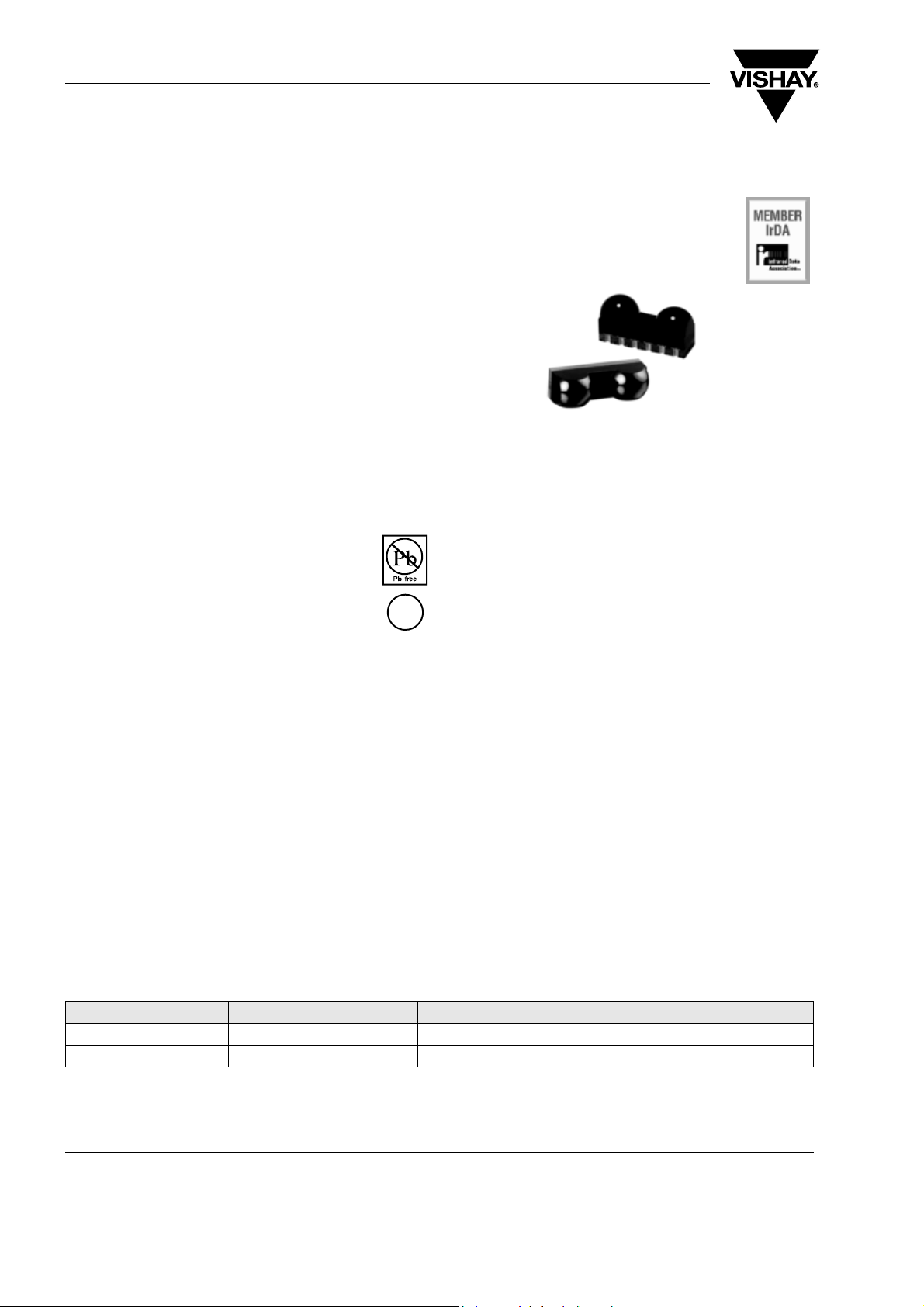
TFBS6711
Vishay Semiconductors
Low Profile Fast Infrared Transceiver (FIR, 4 Mbit/s)
for IrDA
Description
The TFBS6711 is the smallest FIR transceiver available. It is a low profile and low-power IrDA transceiver. Compliant to IrDA’s Physical Layer specification, the TFBS6711 supports data transmission rates
from 9.6 kbit/s to 4 Mbit/s with a typical link distance
of 50 cm. It also enables mobile phones and PDAs to
function as universal remote controls for televisions,
DVDs and other home appliances. The TFBS6711
emitter covers a range of 6.5 meters with common
remote control receivers. Integrated within the transceiver module is a PIN photodiode, an infrared emitter, and a low-power control IC. The TFBS6711 can
be completely shutdown, achieving very low power
consumption. The TFBS6711 has an I/O voltage
®
Applications
related to the supply voltage while TFBS6712 supports low voltage logic of 1.8 V allowing direct connection to a microcontroller’s I/Os operating at 1.8 V.
20208
Features
• Lowest profile: 1.9 mm
• Smallest footprint: 6.0 mm x 3.05 mm
• Surface mount package
• IrDA transmit distance: 50 cm typical
• Best Remote Control distance:
• Fast data rates: from 9.6 kbit/s to 4 Mbit/s
• Low shutdown current: 0.01 µA
• Operating Voltage: 2.4 V to 3.6 V
• Reduced pin count: 6 pins
• I/O voltage equal to the supply voltage
• Pin compatibility: TFBS4711 and TFBS5711
• Integrated EMI Protection
required
≥ 6.5 m on-axis
− no external shield
e4
•IEC 60825-1 Class 1, Eye Safe
• Qualified for Lead (Pb)-free and Sn/Pb processing
• Compliant to IrDA Physical Layer Specification
• Split power supply, transmitter and receiver can be
operated from two power supplies with relaxed
requirements saving costs, US patent
No. 6,157,476
• Lead (Pb)-free device
• Qualified for lead (Pb)-free and Sn/Pb processing
(MSL4)
• Device in accordance with RoHS 2002/95/EC and
WEEE 2002/96/EC
Applications
• High-speed data transfer using infrared
wireless communication
• Mobile phones
• Camera phones
•PDAs
• MP3 Players
• Digital Cameras
• IrDA Adapters or Dongles
Package Options
Ordering Information
Part Number Qty / Reel or Tube Description and Remarks
TFBS6711-TR1 1000 pcs Oriented in carrier tape for side view surface mounting
TFBS6711-TR3 2500 pcs Oriented in carrier tape for side view surface mounting
Note: A version oriented in the carrier tape for top view mounting is available on request
www.vishay.com
258
Document Number 84676
Rev. 1.2, 03-Jul-06

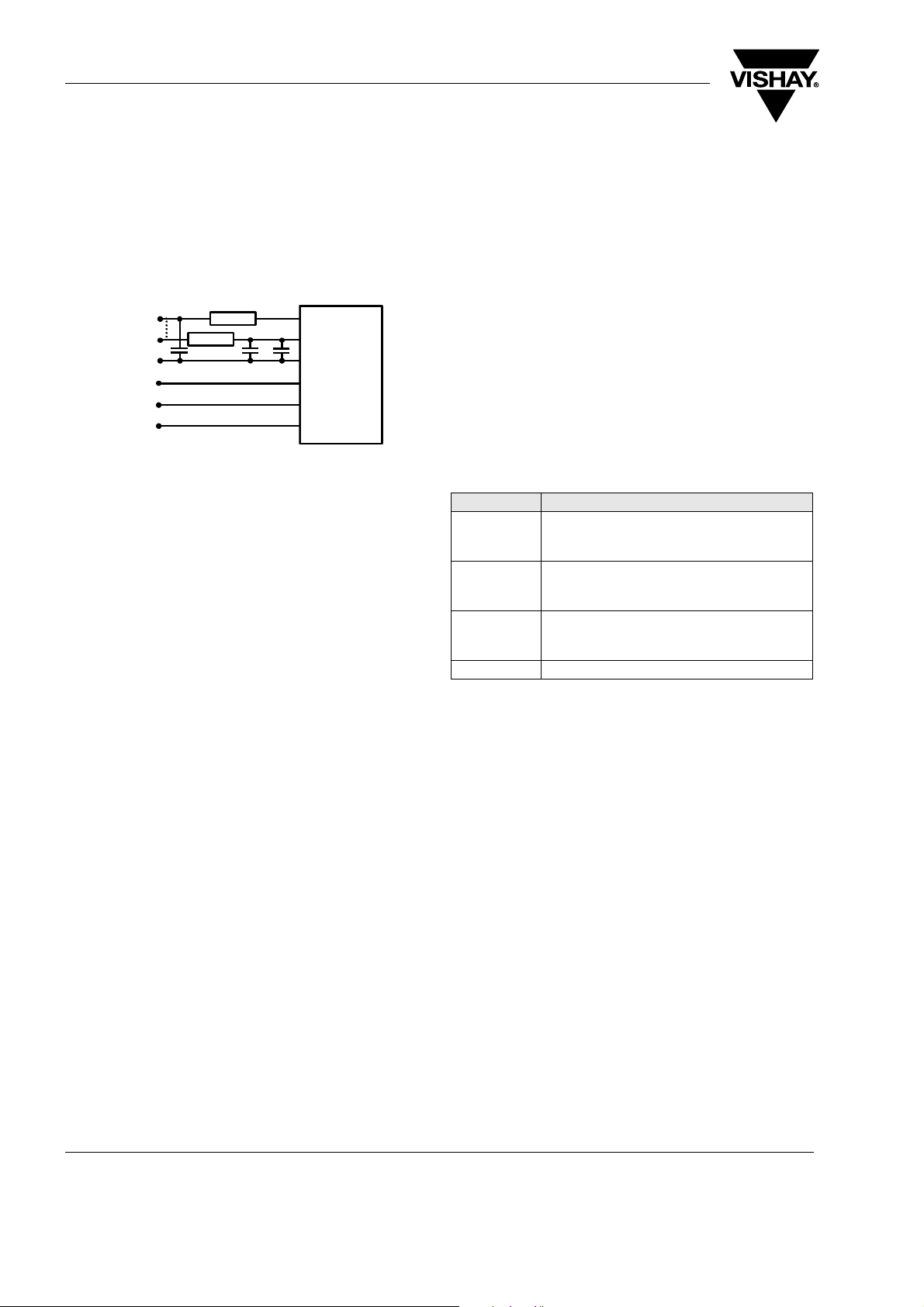
Functional Block Diagram
Amplifier
V
Comparator
CC1
TFBS6711
Vishay Semiconductors
Tri-State
Driver
RXD
V
CC2
SD
Logic
&
Control
Controlled
Driver
TXD
GND
19298
Figure 1. Functional Block Diagramm
Pin Description
Pin Number Function Description I/O Active
1V
2 TXD Transmit Data Input I HIGH
3 RXD Received Data Output, push-pull CMOS driver output capable of driving a
4 SD Shutdown, also used for dynamic mode switching I HIGH
5V
6 GND Ground
CC2
Anode
, IRED
CC1
IRED anode to be externally connected to V
3.6 V an external resistor might be necessary for reducing the internal power
dissipation. See derating curves. This pin is allowed to be supplied from an
uncontrolled power supply separated from the controlled V
standard CMOS load. No external pull-up or pull-down resistor is required.
Floating with a weak pull-up of 500 kΩ (typ.) in shutdown mode. The RXD
output echos the TXD input during transmission.
Supply voltage
. For higher voltages as
CC2
CC1
- supply
OLOW
TFBS6711
Weight: 50 mg
Document Number 84676
Rev. 1.2, 03-Jul-06
PIN 1
Figure 2. Pinning
19428
www.vishay.com
259

TFBS6711
Vishay Semiconductors
Absolute Maximum Ratings
Reference point Pin, GND unless otherwise noted.
Typical values are for DESIGN AID ONLY, not guaranteed nor subject to production testing.
Parame te r Test Conditions Symbol Min Ty p. Max Unit
Supply voltage range,
transceiver
Supply voltage range,
transmitter
0 V < V
0 V < V
< 6 V V
CC2
< 6 V V
CC1
CC1
CC2
Input currents For all Pins, Except IRED Anode
Pin
Output sinking current 25 mA
Power dissipation P
Junction temperature T
Ambient temperature range
(operating)
Storage temperature range T
D
J
T
amb
stg
Soldering temperature 260 °C
Average output current I
Repetitive pulse output current < 90 µs, t
< 20 % I
on
IRED anode voltage I
Voltage at all inputs and outputs V
in
> V
is allowed V
CC1
Virtual source size Method: (1-1/e) encircled
(DC) 125 mA
IRED
(RP) 600 mA
IRED
IREDA
in
d1.5 mm
energy
Maximum Intensity for Class 1 operation of
IEC60825-1 or EN60825-1, edition Jan. 2001
®
IrDA
specified maximum limit
Due to the internal limitation measures the device is a “class 1” device. It will not exceed the IrDA
intensity limit of 500 mW/sr
- 0.5 6 V
- 0.5 6.5 V
10 mA
500 mW
125 °C
- 25 + 85°C
- 25 + 85°C
- 0.5 6.5 V
- 0.5 5.5 V
internal
mW/sr
limitation
to class 1
500
®
Definitions:
In the Vishay transceiver data sheets the following nomenclature is used for defining the IrDA operating modes:
SIR: 2.4 kbit/s to 115.2 kbit/s, equivalent to the basic serial infrared standard with the physical layer version IrPhY 1.0
MIR: 576 kbit/s to 1152 kbit/s
FIR: 4 Mbit/s
VFIR: 16 Mbit/s
®
, the Infrared Data Association, implemented MIR and FIR with IrPHY 1.1, followed by IrPhY 1.2, adding the SIR Low Power Stan-
IrDA
dard. IrPhY 1.3 extended the Low Power Option to MIR and FIR and VFIR was added with IrPhY 1.4. A new version of the standard in any
case obsoletes the former version.
www.vishay.com
260
Document Number 84676
Rev. 1.2, 03-Jul-06

TFBS6711
Vishay Semiconductors
Electrical Characteristics
T
= 25 °C, VCC = 2.4 V to 3.6 V unless otherwise noted.
amb
Typical values are for DESIGN AID ONLY, not guaranteed nor subject to production testing.
Parameters Test Conditions / Pins Symbol Min Ty p. Max Unit
Transceiver
Supply voltage V
CC
Dynamic supply current Receive mode only.
In transmit mode, add additional 85 mA (typ) for IRED current.
Add RXD output current depending on RXD load.
I
SD = Low, SIR mode
SD = Low, MIR/FIR mode I
Shutdown supply current SD = High
T = 25 °C, not ambient light
CC
CC
I
SD
sensitive, detector is disabled in
shutdown mode
Shutdown supply current SD = High
T = 85 °C, not ambient light
I
SD
sensitive
Operating temperature range T
Output voltage low I
Output voltage high I
= 1 mA
OL
C
LOAD
= - 250 µA
OH
C
LOAD
= 15 pF
= 15 pF
Internal RXD pull-up R
Input voltage low (TXD, SD) V
Input voltage high (TXD, SD) V
Input leakage current (TXD, SD) I
Input capacitance
(TXD, SD)
*)
Standard illuminant A
**)
The typical threshold level is 0.5 x VCC (VCC = 3 V). It is recommended to use the specified min/max values to avoid increased operating/
V
V
OL
OH
RXD
IH
ICH
C
A
IL
I
shutdown currents.
2.4 3.6 V
1.7 3 mA
1.9 3.3 mA
1µA
5µA
- 25 + 85°C
0.4 V
0.9 x V
CC
V
400 500 600 kΩ
- 0.5 0.5 V
VCC - 0.5 VCC + 0.5 V
- 1 0.05 + 1 µA
5pF
Document Number 84676
Rev. 1.2, 03-Jul-06
www.vishay.com
261

TFBS6711
Vishay Semiconductors
Optoelectronic Characteristics
T
= 25 °C, VCC = 2.4 V to 3.6 V unless otherwise noted.
amb
Typical values are for DESIGN AID ONLY, not guaranteed nor subject to production testing.
Parameter Test Conditions Symbol Min Ty p . Max Unit
Receiver
Minimum irradiance E
in
e
angular range **)
Minimum irradiance E
in
e
angular range
MIR mode
Minimum irradiance E
in
e
angular range
FIR mode
Maximum irradiance E
in
e
angular range ***)
No detection receiver Input
Irradiance (fluorescent light
noise suppression)
Rise time of output signal 10 % to 90 %, C
Fall time of output signal 90 % to 10 %, C
RXD pulse width of output
signal, 50%, SIR mode
RXD pulse width of output
signal, 50%, MIR mode
RXD pulse width of output
signal, 50%, FIR mode
RXD pulse width of output
signal, 50%, FIR mode
RXD output jitter, leading edge
Receiver start up time After completion of shutdown
9.6 kbit/s to 115.2 kbit/s
λ = 850 nm - 900 nm, V
CC
= 2.4 V
1.152 Mbit/s
λ = 850 nm - 900 nm, V
= 2.4 V
CC
4 Mbit/s
λ = 850 nm - 900 nm, V
= 2.4 V
CC
λ = 850 nm - 900 nm E
= 15 pF t
L
= 15 pF t
L
r (RXD)
f (RXD)
Input pulse length
1.4 μs < P
Wopt
< 25 µs
Input pulse length
P
= 217 ns, 1.152 Mbit/s
Wopt
Input pulse length
P
= 125 ns, 4 Mbit/s
Wopt
Input pulse length
= 250 ns, 4 Mbit/s
P
Wopt
Input irradiance = 150 mW/m
2
,
4 Mbit/s
1.152 Mbit/s
≤ 115.2 kbit/s
E
e 50
E
e 100
E
e 120
e 5
E
e 4
(0.4)
10 50 ns
10 50 ns
t
t
t
t
PW
PW
PW
PW
1.4 1.8 2.6 µs
110 250 270 ns
110 140 ns
225 275 ns
(5)
(10)
(12)
(500)
80
(8)
200
(20)
20
40
350
500 µs
programming sequence
Power on delay
Latency t
Note: All timing data measured with 4 Mbit/s are measured using the IrDA
®
L
FIR transmission header. The data given here are valid 5 µs
100 µs
after starting the preamble.
**)
IrDA sensitivity definition: Minimum Irradiance Ee In Angular Range, power per unit area. The receiver must meet the BER specification while the source is operating at the minimum intensity in angular range into the minimum half-angle range at the maximum Link
Length
***)
Maximum Irradiance Ee In Angular Range, power per unit area. The optical delivered to the detector by a source operating at the
maximum intensity in angular range at Minimum Link Length must not cause receiver overdrive distortion and possible related link errors.
If placed at the Active Output Interface reference plane of the transmitter, the receiver must meet its bit error ratio (BER) specification.
mW/m
(µW/cm
mW/m
(µW/cm
mW/m
(µW/cm
kW/m
(mW/cm
mW/m
(µW/cm
ns
ns
ns
2
2
2
2
2
2
2
2
2
2
)
)
)
)
)
For more definitions see the document “Symbols and Terminology” on the Vishay Website (http://www.vishay.com/docs/82512/82512.pdf
www.vishay.com
262
Document Number 84676
Rev. 1.2, 03-Jul-06
).

TFBS6711
Vishay Semiconductors
Optoelectronic Characteristics, continued
T
= 25 °C, VCC = 2.4 V to 3.6 V unless otherwise noted.
amb
Typical values are for DESIGN AID ONLY, not guaranteed nor subject to production testing.
Parameter Test Conditions Symbol Min Ty p. Max Unit
IRED operating current,
switched current control
Output leakage IRED current V
Output radiant intensity,
s. figure 3, recommended
application circuit
Output radiant intensity,
s. figure 3, recommended
application circuit
Output radiant intensity V
For 3.3-V operation no external
resistor is needed.
= V
CC
V
CC
TXD = High, SD = Low, R
V
CC
TXD = High, SD = Low, R
CC1
= 3.3 V, TXD = Low I
IRED
= V
= 3.3 V, α = 0°
IRED
= V
= 3.3 V, α = 0°, 15°
IRED
= 3.6 V, α = 0°, 15°
= 1 Ω
1
= 1 Ω
1
I
D
IRED
I
e
I
e
I
e
TXD = Low or SD = High
(Receiver is inactive as long as
SD = High)
Output radiant intensity, angle of
α
half intensity
Peak - emission wavelength λ
Optical rise time,
Optical fall time
Optical output pulse duration Input pulse width 217 ns,
t
ropt
t
t
p
,
fopt
opt
1.152 Mbit/s
Optical output pulse duration Input pulse width 125 ns, 4 Mbit/s t
Optical output pulse duration Input pulse width 250 ns, 4 Mbit/s t
Optical output pulse duration Input pulse width t < 80 µs
Input pulse width t ≥ 80 µs
opt
opt
t
opt
t
opt
Optical overshoot 25 %
330 440 600 mA
- 1 1 µA
45 115 300 mW/sr
25 75 300 mW/sr
0.04 mW/sr
±
24
880 900 nm
10 40 ns
200 217 230 ns
116 125 134 ns
241 250 259 ns
t
20
85
°
µs
µs
Document Number 84676
Rev. 1.2, 03-Jul-06
www.vishay.com
263
TFBS6711
S
T
Vishay Semiconductors
Recommended Circuit Diagram
Operated at a clean low impedance power supply the
TFBS6711 needs no additional external components.
However, depending on the entire system design and
board layout, additional components may be required
(see figure 3).
V
CC2
V
CC1
GND
D
XD
RXD
19299
Figure 3. Recommended Application Circuit
C1
R2
C3
R1
C2
The capacitor C1 is buffering the supply voltage and
eliminates the inductance of the power supply line.
This one should be a Tantalum or other fast capacitor
to guarantee the fast rise time of the IRED current.
Vishay transceivers integrate a sensitive receiver and
a built-in power driver. The combination of both needs
a careful circuit board layout. The use of thin, long,
resistive and inductive wiring should be avoided. The
inputs (RXD, SD) and the output RXD should be
directly (DC) coupled to the I/O circuit.
The capacitor C2 combined with the resistor R2 is the
low pass filter for smoothing the supply voltage.
R2, C1 and C2 are optional and dependent on the
quality of the supply voltages V
noise. An unstable power supply with dropping voltage during transmission may reduce the sensitivity
(and transmission range) of the transceiver.
The placement of these parts is critical. It is strongly
recommended to position C2 as close as possible to
the transceiver power supply pins.
A Tantalum capacitor should be used for C1 while a
ceramic capacitor is used for C2.
IRED Anode
V
CC
Ground
SD
TXD
RXD
and injected
CCx
In addition, when connecting the described circuit to
the power supply, low impedance wiring should be
used.
When extended wiring is used the inductance of the
power supply can cause dynamically a voltage drop
at V
. Often some power supplies are not able to
CC2
follow the fast current rise time. In that case another
4.7 µF (type, see table under C1) at V
will be help-
CC2
ful.
Keep in mind that basic RF-design rules for circuit
design should be taken into account. Especially
longer signal lines should not be used without termination. See e.g. "The Art of Electronics" Paul Horowitz, Winfield Hill, 1989, Cambridge University Press,
ISBN: 0521370957.
Table 1. Recommended Application Circuit Components
Component Recommended Value
C1 4.7 µF, 16 V
Vishay part#:
293D 475X9 016B
C2 0.1 µF, Ceramic
Vishay part#:
VJ1206 Y 104 J XXMT
R1 3.3 V supply voltage: no resistor is necessary,
the internal controller is able to control the
current
R2 4.7 Ω, 0.125 W
I/O and Software
In the description, already different I/Os are mentioned. Different combinations are tested and the
function verified with the special drivers available
from the I/O suppliers. In special cases refer to the I/
O manual, the Vishay application notes, or contact
directly Vishay Sales, Marketing or Application.
www.vishay.com
264
Document Number 84676
Rev. 1.2, 03-Jul-06

TFBS6711
Vishay Semiconductors
Mode Switching
The TFBS6711 is in the SIR mode after power on as
a default mode, therefore the FIR data transfer rate
has to be set by a programming sequence using the
TXD and SD inputs as described below. The low frequency mode covers speeds up to 115.2 kbit/s. Signals with higher data rates should be detected in the
high frequency mode. Lower frequency data can also
be received in the high frequency mode but with
reduced sensitivity. To switch the transceivers from
low frequency mode to the high frequency mode and
vice versa, the programming sequences described
below are required.
Setting to the High Bandwidth Mode
(0.576 Mbit/s to 4 Mbit/s)
1. Set SD input to logic "HIGH".
2. Set TXD input to logic "HIGH". Wait t
3. Set SD to logic "LOW" (this negative edge latches
state of TXD, which determines speed setting).
4. After waiting t
≥ 200 ns TXD can be set to logic
h
“LOW”. The hold time of TXD is limited by the maximum allowed pulse length.
TXD is now enabled as normal TXD input for the high
bandwidth mode.
≥ 200 ns.
s
Setting to the Lower Bandwidth Mode
(2.4 kbit/s to 115.2 kbit/s)
1. Set SD input to logic "HIGH".
2. Set TXD input to logic "LOW". Wait t
3. Set SD to logic "LOW" (this negative edge latches
state of TXD, which determines speed setting).
4. TXD must be held for t
≥ 200 ns.
h
TXD is now enabled as normal TXD input for the
lower bandwidth mode.
SD
TXD
50 %
Figure 4. Mode Switching Timing Diagram
50 %
t
t
s
h
50 %
≥ 200 ns.
s
Hig h:F IR
Low : SIR
14873
Truth table
Inputs Outputs
SD TXD Input irradiance mW/m
high x x weakly pulled
low high x high I
low high > 80 µs x high 0
low low < 4 high 0
low low > Min. irradiance E
in angular range
< Max. irradiance E
in angular range
low low > Max. irradiance E
in angular range
Document Number 84676
Rev. 1.2, 03-Jul-06
2
e
e
e
RXD Transmitter
0
(500 kΩ)
high
e
low (active) 0
x0
www.vishay.com
265

TFBS6711
0
20
40
60
80
100
120
140
160
180
200
220
240
260
0 50 100 150 200 250 300 350
Time/s
Tem peratu re/°C
2...4 °C/s
2...4 °C/s
10 s max. at 230 °C
120 s...180 s
160 °C max.
240 °C max.
90 s max.
20
Vishay Semiconductors
Recommended Solder Profiles
Solder Profile for Sn/Pb soldering
Figure 5. Recommended Solder Profile for Sn/Pb soldering
19431
Manual Soldering
Manual soldering is the standard method for lab use.
However, for a production process it cannot be recommended because the risk of damage is highly
dependent on the experience of the operator. Nevertheless, we added a chapter to the above mentioned
application note, describing manual soldering and
desoldering.
Storage
The storage and drying processes for all VISHAY
transceivers (TFDUxxxx and TFBSxxx) are equivalent to MSL4.
The data for the drying procedure is given on labels
on the packing and also in the application note
"Taping, Labeling, Storage and Packing"
(http://www.vishay.com/docs/8 2601/82601.pdf).
Lead (Pb)-Free, Recommended Solder Profile
The TFBS6711 is a lead (Pb)-free transceiver and
qualified for lead (Pb)-free processing. For lead
(Pb)-free solder paste like Sn(3.0-4.0)Ag(0.5-0.9)Cu,
there are two standard reflow profiles: Ramp-SoakSpike (RSS) and Ramp-To-Spike (RTS). The RampSoak-Spike profile was developed primarily for reflow
ovens heated by infrared radiation. With widespread
use of forced convection reflow ovens the Ramp-ToSpike profile is used increasingly. Shown below in
figure 6 is VISHAY's recommended profiles for use
with the TFBS6711 transceivers. For more details
please refer to Application note: SMD Assembly
Instruction.
Wave Soldering
For TFDUxxxx and TFBSxxxx transceiver devices
wave soldering is not recommended.
280
260
240
220
200
180
160
140
120
Temperature/°C
100
80
60
2 °C...4 °C/s
40
20
0
0 50 100 150 200 250 300 350
19261
T ≥ 255 °C for 20 s max
T ≥ 217 °C for 50 s max
90 s...120 s
Time/s
s
50 s max.
T
peak
= 260 °C max.
Figure 6. Solder Profile, RSS Recommendation
2 °C...4 °C/s
www.vishay.com
266
Document Number 84676
Rev. 1.2, 03-Jul-06

TFBS4711, TFBS5711, TFBS6711, and TFBS6712 Package
(Mechanical Dimensions)
TFBS6711
Vishay Semiconductors
19612
Figure 7. Package drawing, tolerances: Height + 0.1, - 0.2 mm, otherwise ± 0.2 mm if not indicated
19728
Soldering footprint: Side view
Figure 8. Soldering footprints
19301
Soldering footprint: Top view
Design Rules for Optical Windows
For optical windows see the application note on the web http://www.vishay.com/docs/82506/82506.pdf
Document Number 84676
Rev. 1.2, 03-Jul-06
.
www.vishay.com
267
TFBS6711
Vishay Semiconductors
Drawing-No.: 9.800-5090.01-4
Issue: 1; 29.11.05
14017
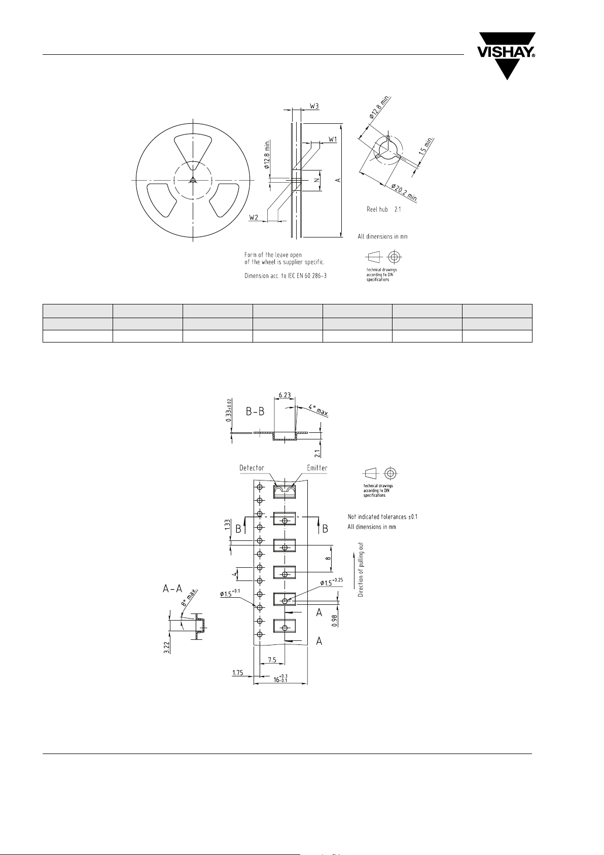
Tape Width A max. N W1 min. W2 max. W3 min. W3 max.
mm mm mm mm mm mm mm
16 330 50 16.4 22.4 15.9 19.4
Figure 9. Reel dimensions [mm]
Drawing-No.: 9.700-5294.01-4
Issue: prel. copy; 24.11.04
www.vishay.com
268
19303
Figure 10. Tape dimensions [mm] TFBS6711-TT3
Document Number 84676
Rev. 1.2, 03-Jul-06

TFBS6711
Vishay Semiconductors
Drawing-No.: 9.700-5295.01-4
Issue: prel. copy; 24.11.04
19304
Figure 11. Tape dimensions [mm] TFBS6711-TR3
Document Number 84676
Rev. 1.2, 03-Jul-06
www.vishay.com
269

TFBS6711
Vishay Semiconductors
Ozone Depleting Substances Policy Statement
It is the policy of Vishay Semiconductor GmbH to
1. Meet all present and future national and international statutory requirements.
2. Regularly and continuously improve the performance of our products, processes, distribution and operating
systems with respect to their impact on the health and safety of our employees and the public, as well as
their impact on the environment.
It is particular concern to control or eliminate releases of those substances into the atmosphere which are
known as ozone depleting substances (ODSs).
The Montreal Protocol (1987) and its London Amendments (1990) intend to severely restrict the use of ODSs
and forbid their use within the next ten years. Various national and international initiatives are pressing for an
earlier ban on these substances.
Vishay Semiconductor GmbH has been able to use its policy of continuous improvements to eliminate the use
of ODSs listed in the following documents.
1. Annex A, B and list of transitional substances of the Montreal Protocol and the London Amendments
respectively
2. Class I and II ozone depleting substances in the Clean Air Act Amendments of 1990 by the Environmental
Protection Agency (EPA) in the USA
3. Council Decision 88/540/EEC and 91/690/EEC Annex A, B and C (transitional substances) respectively.
Vishay Semiconductor GmbH can certify that our semiconductors are not manufactured with ozone depleting
substances and do not contain such substances.
We reserve the right to make changes to improve technical design
and may do so without further notice.
Parameters can vary in different applications. All operating parameters must be validated for each
customer application by the customer. Should the buyer use Vishay Semiconductors products for any
unintended or unauthorized application, the buyer shall indemnify Vishay Semiconductors against all
claims, costs, damages, and expenses, arising out of, directly or indirectly, any claim of personal
damage, injury or death associated with such unintended or unauthorized use.
Vishay Semiconductor GmbH, P.O.B. 3535, D-74025 Heilbronn, Germany
Document Number 84676
Rev. 1.2, 03-Jul-06
www.vishay.com
270

Legal Disclaimer Notice
Vishay
Document Number: 91000 www.vishay.com
Revision: 08-Apr-05 1
Notice
Specifications of the products displayed herein are subject to change without notice. Vishay Intertechnology, Inc.,
or anyone on its behalf, assumes no responsibility or liability for any errors or inaccuracies.
Information contained herein is intended to provide a product description only. No license, express or implied, by
estoppel or otherwise, to any intellectual property rights is granted by this document. Except as provided in Vishay's
terms and conditions of sale for such products, Vishay assumes no liability whatsoever, and disclaims any express
or implied warranty, relating to sale and/or use of Vishay products including liability or warranties relating to fitness
for a particular purpose, merchantability, or infringement of any patent, copyright, or other intellectual property right.
The products shown herein are not designed for use in medical, life-saving, or life-sustaining applications.
Customers using or selling these products for use in such applications do so at their own risk and agree to fully
indemnify Vishay for any damages resulting from such improper use or sale.
 Loading...