

Page 1
TELEFUNKEN
Semiconductors
TFDU6100E/TFDS6500E/TFDT6500E
2.7–5.5V Fast Infrared Transceiver Module Family
(FIR, 4 Mbit/s)
Features Applications
Compliant to IrDA 1.2 (Up to
4 Mbit/s), HP–SIR, Sharp ASK
and TV Remote
Wide Operating Voltage Range
(2.7 to 5.5 V )
Low-Power Consumption (3 mA
Supply Current)
Power Shutdown Mode (1 A
Shutdown Current)
Long Range (Up to 2.0 m at
4 Mbit/s in Nominal Design)
High Efficiency Emitter
(120 mW/sr min 15)
Three Surface Mount Package
Options
– Universal (9.7 x 4.7 x 4.0 mm)
– Side View (13.0 x 5.95 x 5.3 mm)
– T op View (13.0 x 7.6 x 5.95 mm)
BabyFace (Universal) Package
Capable of Surface Mount
Solderability to Side and T op
View Orientation
Directly Interfaces With Various
Super I/O and Controller Devices
Built–In EMI Protection – No
External Shielding Necessary
Few External Components
Required
Backward Compatible to All
TEMIC SIR and FIR Infrared
Transceivers
Description
The TFDU6100E, TFDS6500E, and TFDT6500E are a
family of low-power infrared transceiver modules
compliant to the IrDA 1.2 standard for fast infrared (FIR)
data communication, supporting IrDA speeds up to 4.0
Mbit/s, HP–SIR, Sharp ASK and carrier based remote
control modes up to 2 MHz. Integrated within the
transceiver modules are a photo PIN diode, infrared
emitter (IRED), and a low-power CMOS control IC to
provide a total front–end solution in a single package.
TEMIC’s FIR transceivers are available in three package
options, including our BabyFace package (TFDU6100E),
the smallest FIR transceiver available on the market. This
Notebook Computers, Desktop
PCs, Palmtop Computers (Win
CE, Palm PC), PDAs
Digital Still and Video Cameras
Printers, Fax Machines,
Photocopiers, Screen Projectors
T elecommunication Products
(Cellular Phones, Pagers)
Internet TV Boxes, Video
Conferencing Systems
External Infrared Adapters
(Dongles)
Medical and Industrial Data
Collection Devices
wide selection provides flexibility for a variety of
applications and space constraints.
The transceivers are capable of directly interfacing with
a wide variety of I/O chips which perform the pulse-width
modulation/demodulation function, including National
Semiconductor’s PC87338, PC87108 and PC87109,
SMSC’s FDC37C669, FDC37N769 and CAM35C44,
and Hitachi’s SH3. At a minimum, a current-limiting
resistor in series with the infrared emitter and a V
bypass capacitor are the only external components
required to implement a complete solution.
CC
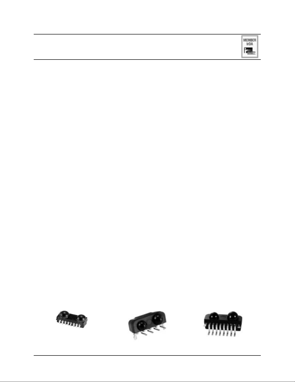
Package Options
TFDU6100E
Baby Face (Universal)
This product is currently in devleopment. Inquiries regarding the status of this product should be directed to TEMIC Marketing.
Pending—Rev. A, 03-Apr-98 1
TFDS6500E
Side View
TFDT6500E
Top View
Pre-Release Information
Page 2
TFDU6100E/TFDS6500E/TFDT6500E
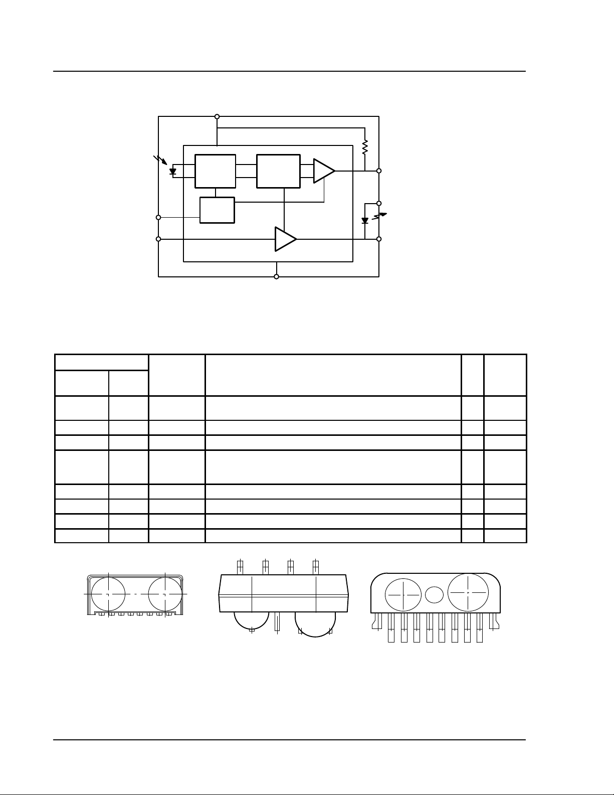
Functional Block Diagram
V
CC
Driver
Amplifier Comparator
TELEFUNKEN
Semiconductors
Rxd
IRED Anode
IRED Cathode
SD/Mode
Txd
AGC
Logic
Open Collector Driver
GND
Pin Assignment and Description
Pin Number
“ U ”, “ T ”
Option
1 8 IRED Anode IRED anode, should be externally connected to VCC through a current
2 1 IRED Cathode IRED cathode, internally connected to driver transistor
3 7 Txd Transmit Data Input I HIGH
4 2 Rxd Received Data Output, push–pull CMOS driver output capable of driving a
5 6 SD/Mode Shutdown/Mode I HIGH
6 3 V
7 5 NC Do not connect.
8 4 GND Ground
“ S ”
Option
Function Description I/O Active
control resistor
standard CMOS or TTL load. No external pull–up or pull–down resistor is
required (pin is floating when device is in shutdown mode).
CC
Supply Voltage
O LOW
5678
IRED Detector
12345678
”U” Option
BabyFace (Universal)
123 4
IRED Detector
”S” Option
Side View
IRED Detector
1 2345678
”T” Option
Top View
2 Pending—Rev . A, 03-Apr-98
Pre-Release Information
Page 3
TELEFUNKEN
V
A
°C
A
Semiconductors
TFDU6100E/TFDS6500E/TFDT6500E
Ordering Information
Part Number Qty/ Reel Description
TFDU6100E–TR3 1000 pcs Oriented in carrier tape for side view surface mounting
TFDU6100E–TT3 1000 pcs Oriented in carrier tape for top view surface mounting
TFDS6500E–TR3 750 pcs
TFDT6500E–TR3 750 pcs
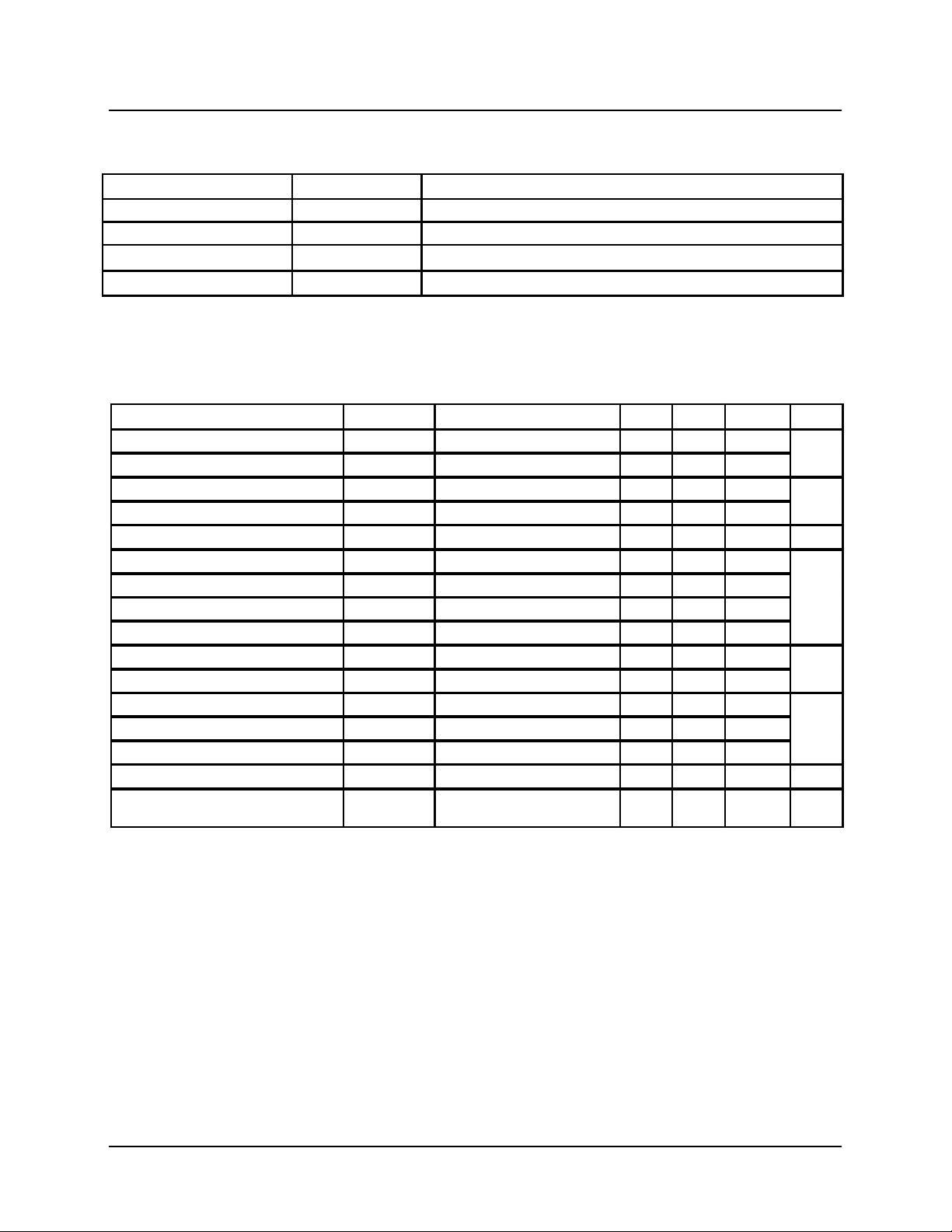
Absolute Maximum Ratings
Parameter Symbol Test Conditions
Supply Voltage Range V
Supply Voltage Range (Anode) V
Input Currents
Output Sinking Current 25
Power Dissipation
Junction Temperature T
Ambient Temperature Range (Operating) T
Storage Temperature Range T
Soldering Temperature See Recommended Solder Profile 240
Average Output Current I
Repetitive Pulsed Output Current I
IRED Anode Voltage at Current Output V
Transmitter Data Input Voltage V
Receiver Data Output Voltage V
Virtual Source Size
Maximum Intensity for Class 1 Operation
of IEC 825 or EN60825
Notes
a. Reference point GND pin unless otherwise noted.
b. The algebraic convention whereby the most negative value is a minimum and the most positive a maximum.
c. Typical values are for DESIGN AID ONLY, not guaranteed nor subject to production testing.
d. Maximum input current for all pins (except IRED Anode pin).
e. See Derating Curve.
f. Method: (1-1/e) encircled energy.
g. Worst case IrDA SIR pulse pattern.
d
e
f
g
CC
anode
P
D
J
amb
stg
(DC) 130
IRED
(RP) <90 µs, ton <20% 600
IRED
IREDA
Txd
Rxd
d 2.5 2.8 mm
EN60825, 1997 320 mW/sr
a
MinbTyp
– 0.5 6
0 VCC+1.5
–25 85
–25 85
– 0.5 6
– 0.5 VCC+0.5
– 0.5 VCC+0.5
c
Max
b
Unit
10
350 mW
125
m
°
m
V
Pending—Rev. A, 03-Apr-98 3
Pre-Release Information
Page 4
TFDU6100E/TFDS6500E/TFDT6500E
A
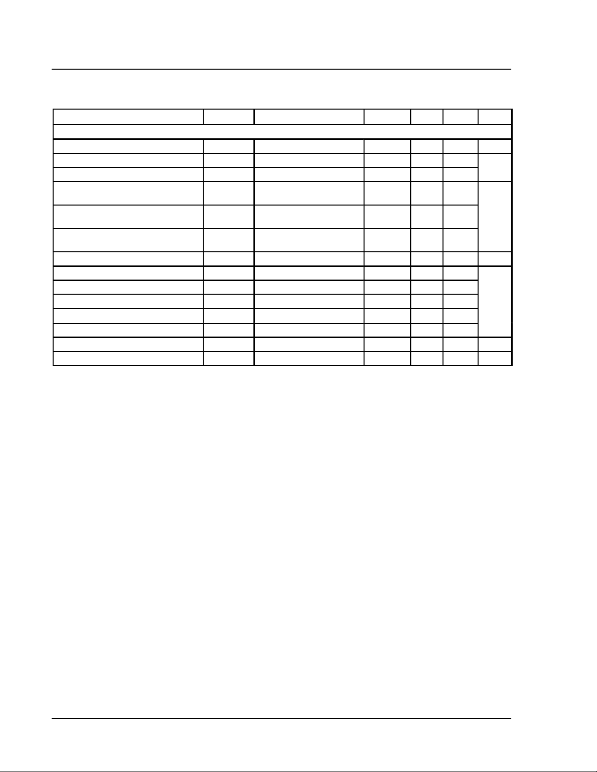
Electrical Characteristics
TELEFUNKEN
Semiconductors
Parameter Symbol Test Conditions
a
Min
b
Transceiver
Supply Voltage V
Dynamic Supply Current
d
Dynamic Supply Current I
Standby Supply Current
e
Standby Supply Current I
Standby Supply Current
e
Operating Temperature Range T
Output Voltage Low V
Output Voltage High V
Input Voltage Low V
Input Voltage High
Input Voltage High
f
g
Input Leakage Current I
Input Capacitance C
Notes
a. Tamb = 25, V
b. The algebraic convention whereby the most negative value is a minimum and the most positive a maximum.
= 2.7 – 5.5 V unless otherwise noted.
CC
CC
I
CC
CC
I
SD
SD
I
SD
A
OL
OH
IL
V
IH
V
IH
L
I
SD = Low, Ee = 0 mW/m
SD = Low, Ee = 1 klx
SD = High, Mode = floating,
25°C, E
= 0 klx
e
SD = High, Mode = floating,
T =25°C, E
= 1 klx
e
SD = High, Mode = floating,
T = 85°C
R
= 2.2 kΩ, C
load
R
load
= 2.2 kΩ, C
load
load
V
≥ 4.5V 2.4
CC
2
d
d
= 15 pF 0.5 0.8
= 15 pF VCC–0.5
2.7 5.5 V
–25 85 °C
0 0.8
0.9 * V
CC
–10 +10 µA
c. Typical values are for DESIGN AID ONLY, not guaranteed nor subject to production testing.
d. Receive mode only. In transmit mode, add additional 100 mA (typ) to IRED current.
e. Not ambient light sensitive.
f. CMOS levels.
g. TTL levels.
TypcMax
3 4
3 4
1
1.5
5
5 pF
b
Unit
m
µA
V
4 Pending—Rev . A, 03-Apr-98
Pre-Release Information
Page 5
TELEFUNKEN
2
Semiconductors
TFDU6100E/TFDS6500E/TFDT6500E
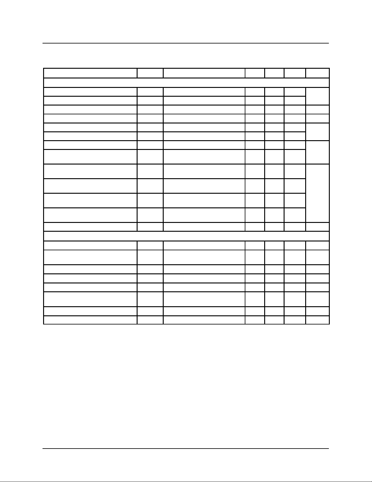
Optoelectronic Characteristics
Parameter Symbol Test Conditions
a
MinbTypcMax
b
Receiver
Minimum Detection Threshold Irradiance E
Minimum Detection Threshold Irradiance E
Maximum Detection Threshold Irradiance E
Logic LOW Receiver Input Irradiance E
Rise Time of Output Signal t
Fall Time of Output Signal t
Rx Pulse Width of Output Signal, 50% P
Rx Pulse Width of Output Signal, 50% P
Rx Pulse Width of Output Signal, 50% P
Rx Pulse Width of Output Signal, 50% P
Rx Pulse Width of Output Signal, 50% P
Jitter, Leading Edge
Latency t
e
e
e
e
RR
FR
w
w
w
w
w
L
9.6 kbit/s to 115.2 kbit/s 20 35
1.152 Mbit/s to 4 Mbit/s 50 80
5 10 kW/m
4 mW/m
10% to 90%, @2.2 kΩ, 15pF 10 40
90% to 10%, @2.2 kΩ, 15pF 10 40
Input pulse length 20 µs, 9.6 kbit/s 1.2 10 20
Input pulse length 1.41µs, 115.2 kbit/s
mode
Input pulse length 217 ns, 4.0 Mbit/s
mode
Input pulse length 125 ns, 4.0 Mbit/s
mode
Input pulse length 250 ns, 4.0 Mbit/s
mode (double pulse)
Input Irradiance = 90 mW/m2,
4.0 Mbit/s mode
1.2 2.2
190 260
90 165
210 290
mW/m
10
120 µs
Transmitter
IRED Operating Current I
Output Radiant Intensity
Output Radiant Intensity Half Angle α ±24
Output Radiant Intensity
Peak Wavelength λ
Voltage drop at output driver
Rise Time, Fall Time tR, t
Optical Overshoot 25 %
Notes
= 25C, VCC = 2.7 – 5.5 V unless otherwise noted.
a. T
amb
b. The algebraic convention whereby the most negative value is a minimum and the most positive a maximum.
c. Typical values are for DESIGN AID ONLY, not guaranteed nor subject to production testing.
d. VCC = 5 V, a = 0, 15
e. Receiver is inactive as long as SD = High
d
d
D
I
e
I
e
P
F
VCC = 5 V, R1= 5.6 Ω 0.48 0.55 A
Txd = High, SD = Low,
R
= 5.6 Ω
1
Txd = Low or SD = Highe, RL=5.6 Ω .04 mW/sr
I
= 600 mA, pulse length 2 µs, duty
F
cycle 25%
120 140 280 mW/sr
880 900 nm
400 800 mV
10 40 ns
Unit
2
2
2
ns
µs
ns
Pending—Rev. A, 03-Apr-98 5
Pre-Release Information
Page 6
TFDU6100E/TFDS6500E/TFDT6500E
Recommended Circuit Diagram
TELEFUNKEN
Semiconductors
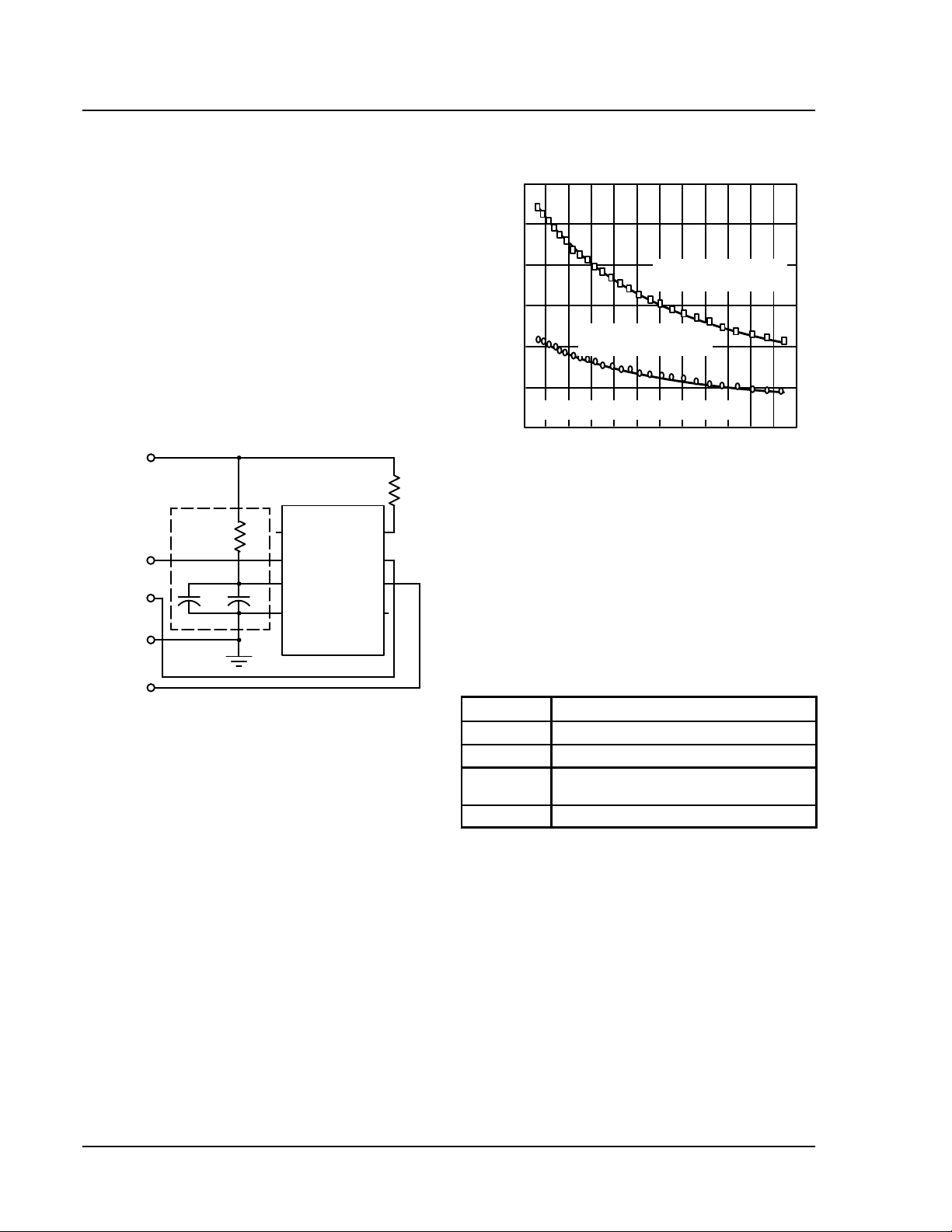
The only required components for designing an IrDA 1.2
compatible design using TEMIC FIR transceivers are a
current limiting resistor, R
, to the IRED. However,
1
depending on the entire system design and board layout,
additional components may be required (see Figure 1).
TEMIC FIR transceivers integrate a sensitive receiver
and a built–in power driver. The combination of both
needs a careful circuit board layout. The use of thin, long
resistive and inductive wiring should be avoided. The
inputs (Txd, SD/Mode) and the output Rxd should be
directly (DC) coupled to the I/O circuit.
V
CC2
R1
Rxd
Txd
GND
R2
C1 C2
TFDx6x00
IRED
Cathode
Rxd
V
CC
GND
IRED
Anode
Txd
SD/Mode
NC
300
250
200
150
Intensity (mW/sr)
100
50
IrDA Field of View: Cone of 15
0
4.0 6.0 8.0 10.0 12.0 14.0 16.0
4.75 V, Min. Efficiency,
Min. VF, Max. R
Current Control Resistor (W)
Figure 2. Ie vs. R
5.25 V, Min. Efficiency ,
Min. VF, Min. R
DSon
DSon
l
The placement of these parts is critical. It is strongly
recommended to position C2 as near as possible to the
transceiver power supply pins. A tantalum capacitor
should be used for C1 while a ceramic capacitor is used
for C2. Also, when connecting the described circuit to the
power supply, low impedance wiring should be used.
SC
Note: Outlined components are optional depending on quality of
power supply.
Figure 1. Recommended Application Circuit
R1 is used for controlling the current through the IR
emitter. For increasing the output power of the IRED, the
value of the resistor should be reduced. Similarly, to
reduce the output power of the IRED, the value of the
resistor should be increased. For typical values of R1 see
Figure 2 . For IrDA compliant operation, a current control
resistor of 5.6 Ω is recommended. The upper drive current
limitation is dependent on the duty cycle and is given by
the absolute maximum ratings on the data sheet.
R2, C1 and C2 are optional and dependent on the quality
of the supply voltage V
and injected noise. An unstable
CC
power supply with dropping voltage during transmission
may reduce sensitivity (and transmission range) of the
transceiver.
Table 1. Recommended Application Circuit Components
Component Recommended Value
C1 4.7 mF, Tantalum
C2 0.1 µF, Ceramic
R1 5.6 Ω , 0.25 W (recommend using two 0.125 W
resistors in parallel)
R2 47 Ω , 0.125 W
Mode Switching
The TFDU6100E, TFDS6500E and TFDT6500E powers
on in a no default mode, therefore the data transfer rate
has to be set by a programming sequence as described
below or selected by setting the mode pin. When using the
Mode pin, the standby current might be increased to about
50 to 60 µA. In standby mode, the mode input should float
to minimize standby current.
The low frequency mode covers speeds up to 115.2 kbit/s.
Signals with higher data rates should be detected in the
high frequency mode. Lower data frequency data can also
6 Pending—Rev . A, 03-Apr-98
Pre-Release Information
Page 7
TELEFUNKEN
Semiconductors
TFDU6100E/TFDS6500E/TFDT6500E
received in high frequency mode with reduced sensitivity .
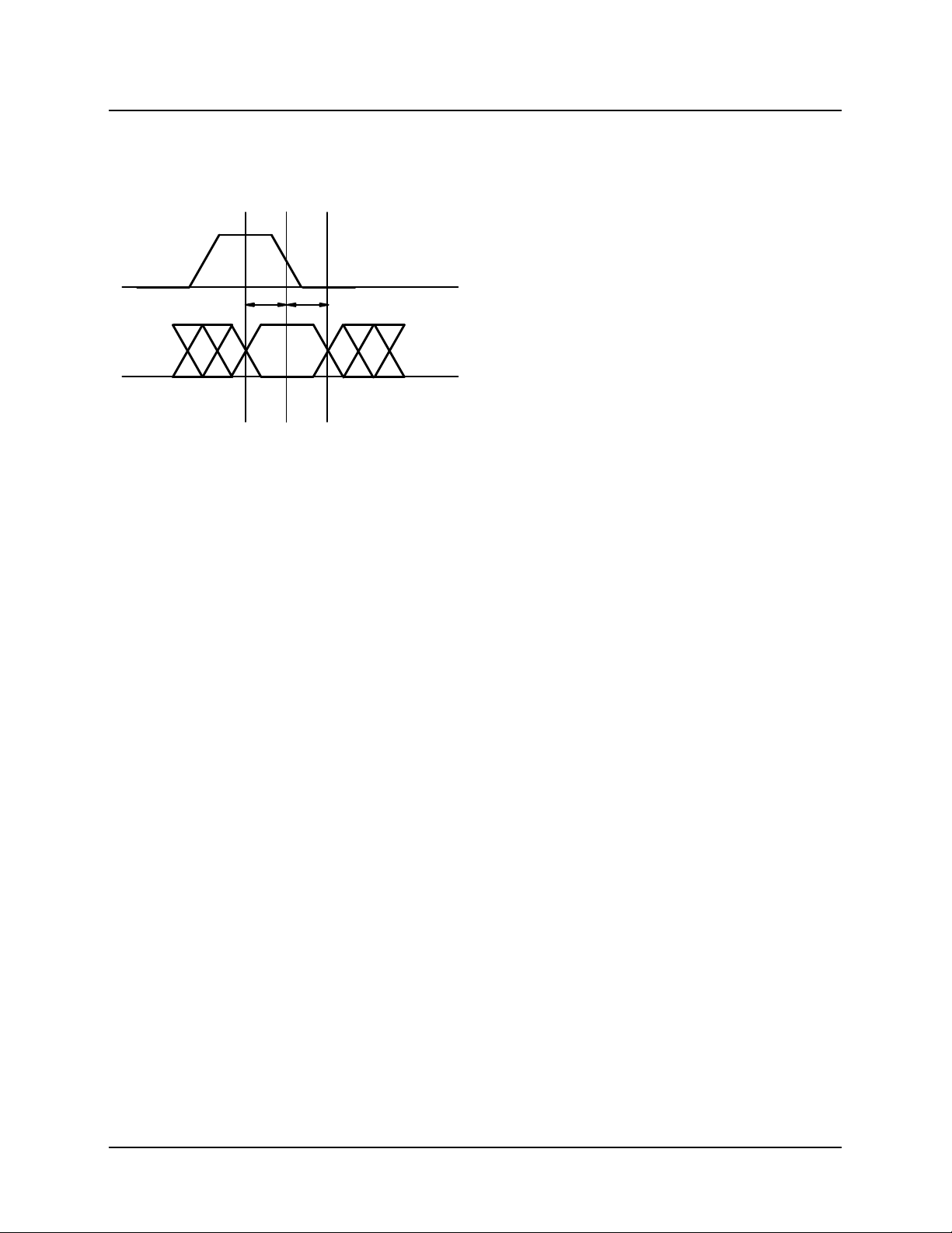
To switch the transceivers from low frequency mode to
the 4.0 Mbit/s mode and vice versa, the programming
sequences described below are required.
SD/Mode
t
t
s
h
High
Txd
Low
Mode Pin
Figure 3. Timing Diagram
High: FIR
Low: SIR
Setting to the High Bandwidth Mode (0.576 to
4.0 Mbit/s)
1. Set SD/MODE input to logic ”HIGH”.
2. Set Txd input to logic ”HIGH”. Wait t
w200 ns.
s
3. Set SD/MODE to logic ”LOW” (this negative edge
latches state of Txd, which determines speed setting).
4. After waiting t
w200 ns Txd can be set to logic
h
”LOW”. The hold time of Txd is limited by the
maximum allowed pulse length.
Txd is now enabled as normal Txd input for the high
bandwidth mode.
Setting to the Lower Bandwidth Mode (2.4 to
115.2 kbit/s)
1. Set SD/MODE input to logic ”HIGH”.
2. Set Txd input to logic ”LOW”. Wait t
3. Set SD/MODE to logic ”LOW” (this negative edge
latches state of Txd, which determines speed setting).
4. Txd must be held for t
w200 ns.
h
Txd is now enabled as normal Txd input for the lower
bandwidth mode.
w200 ns.
s
Pending—Rev. A, 03-Apr-98 7
Pre-Release Information
Page 8
TFDU6100E/TFDS6500E/TFDT6500E
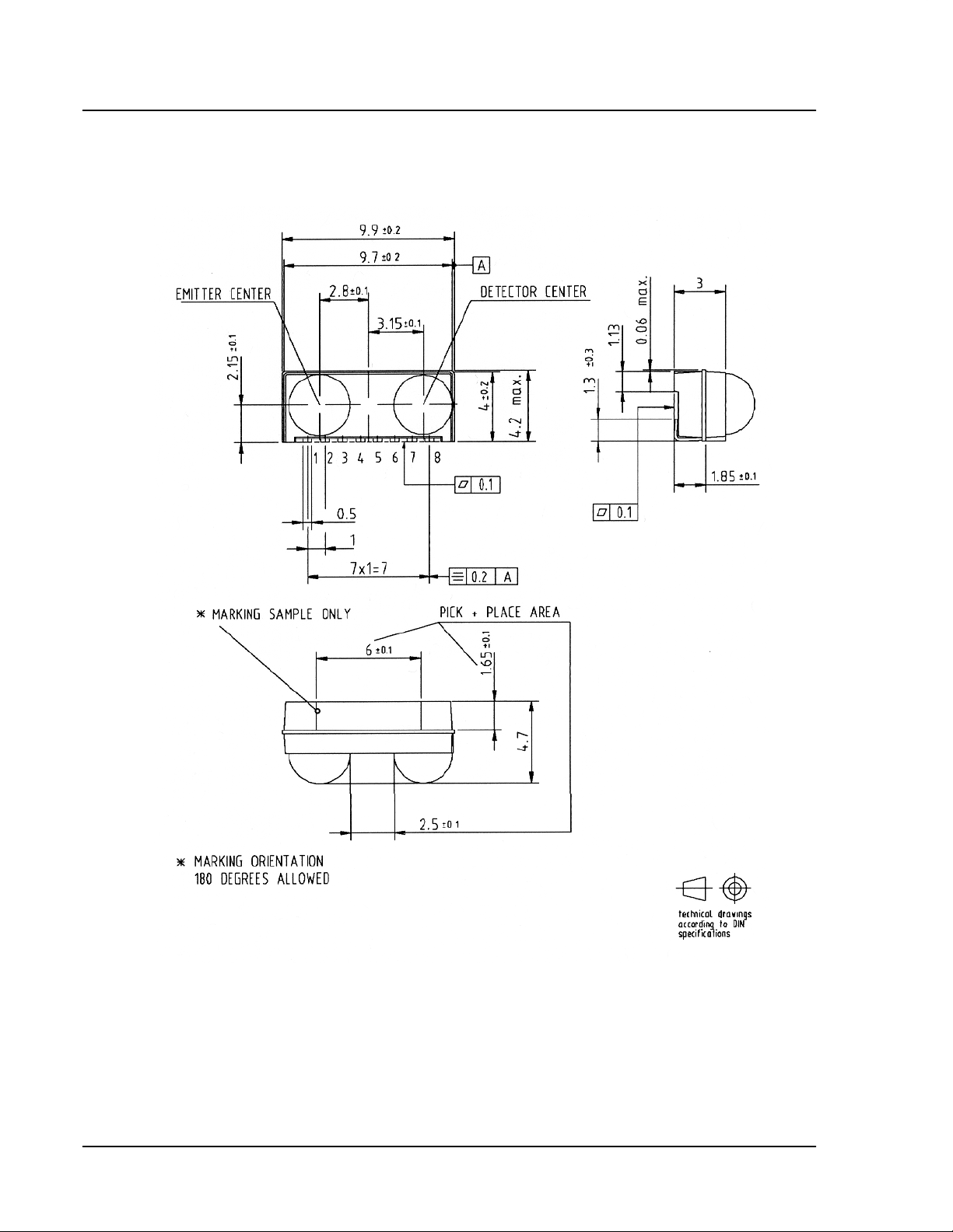
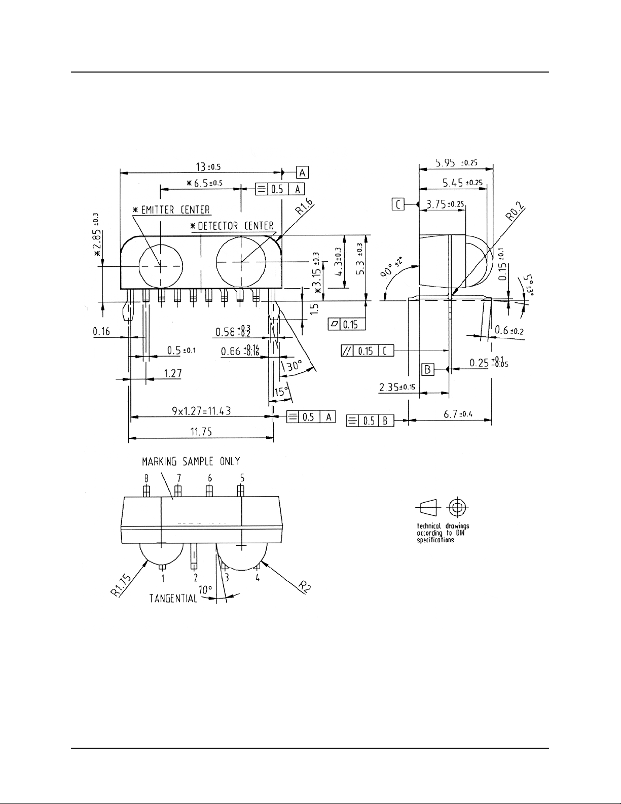
TFDU6100E – BabyFace (Universal) Package
Mechanical Dimensions
TELEFUNKEN
Semiconductors
8 Pending—Rev . A, 03-Apr-98
Pre-Release Information
Page 9
TELEFUNKEN
Semiconductors
TFDU6100E/TFDS6500E/TFDT6500E
TFDS6500E – Side View Package
Mechanical Dimensions
TK84 731
TFDS6500
Pending—Rev. A, 03-Apr-98 9
Pre-Release Information
Page 10
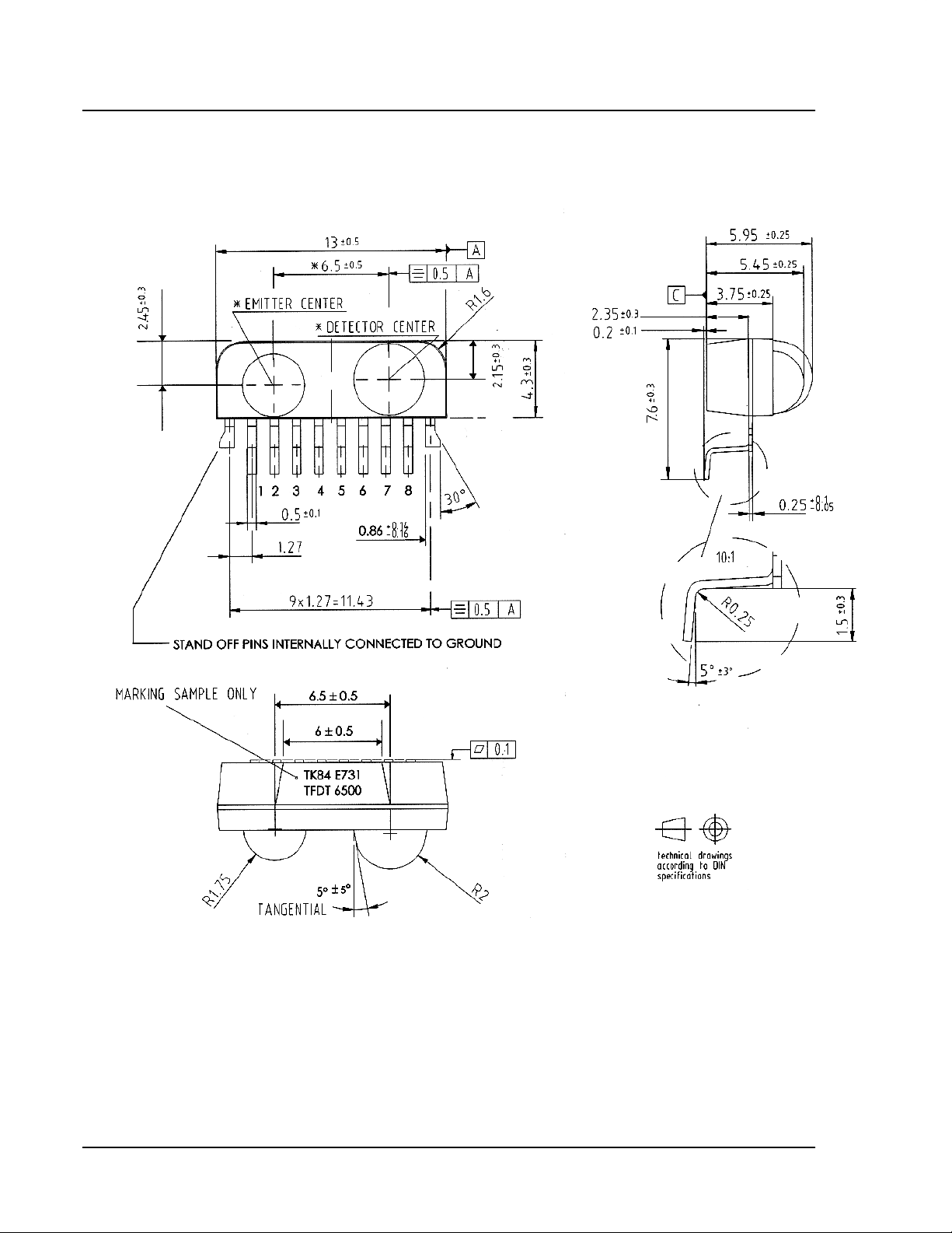
TFDU6100E/TFDS6500E/TFDT6500E
TFDT6500E – Top View Package
Mechanical Dimensions
TELEFUNKEN
Semiconductors
10 Pending—Rev. A, 03-Apr-98
Pre-Release Information
Page 11
TELEFUNKEN
Semiconductors
TFDU6100E/TFDS6500E/TFDT6500E
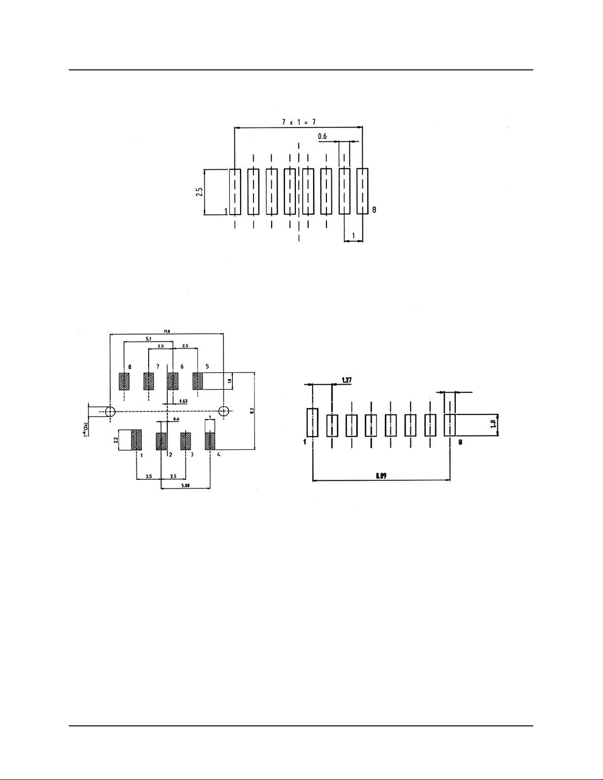
Recommended SMD Pad Layout
TFDU6100E - BabyFace (Universal) Package
a
TFDS6500E - Side View Package
a. The leads of the device should be sodered in the center position pads.
(note: leads of the device should be at least 0.3 mm
within the ends of the pads. Pad 1 is longer to designate
0.8
TFDT6500E - Top View Package
Pin 1 connection to transceiver.)
Pending—Rev. A, 03-Apr-98 11
Pre-Release Information
Page 12
TFDU6100E/TFDS6500E/TFDT6500E
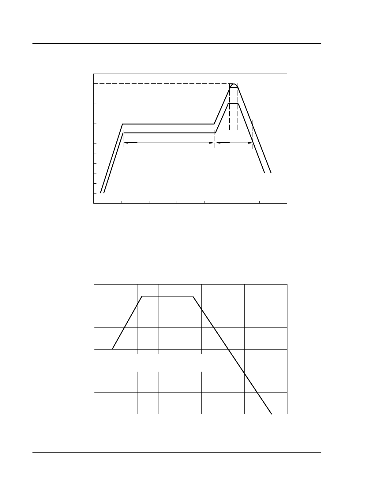
Recommended Solder Profile
260
240
220
200
180
Temperature ( C)
160
140
120
100
80
60
40
20
120 – 180 Seconds 90 s Max.
2 – 4 C/Seconds
0
0 50 100 150 200 250 300 350
2 – 4 C/Seconds
TELEFUNKEN
Semiconductors
10 s Max. @ 230 C
Current Derating Curve
600
500
400
300
Current derating as a function of the
200
Peak Operating Current (mA)
100
maximum forward current of IRED.
Maximum duty cycle: 25%
Time (Seconds)
0
–40 –20 0 20 40 60 80 100
Temperature (C)
120 140
12 Pending—Rev. A, 03-Apr-98
Pre-Release Information
 Loading...