VISHAY
18088
TFBS6614
Vishay Semiconductors
Lowest Profile 4 Mbits/s (FIR) Infrared Transceiver Module
Description
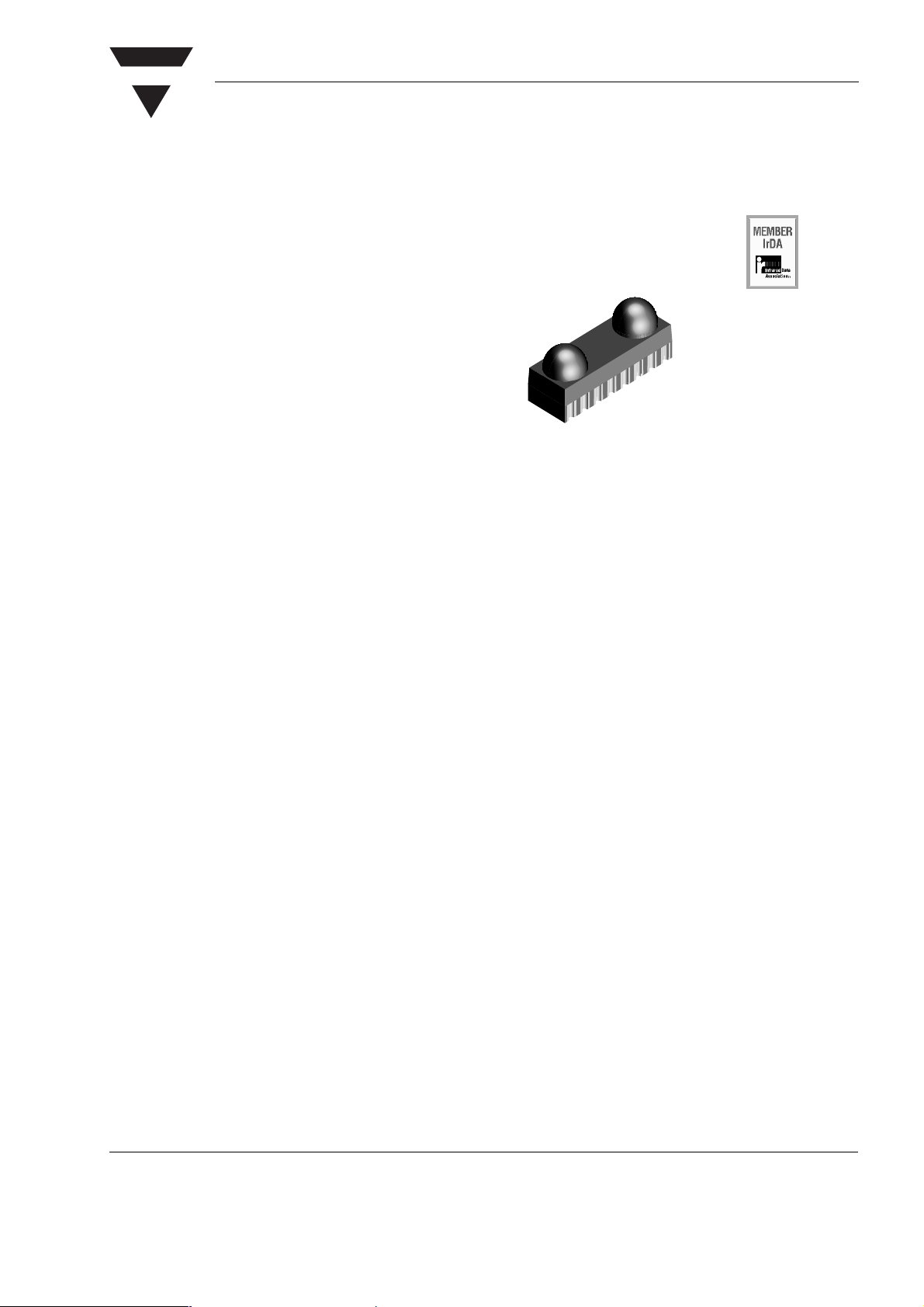
The Vishay TFBS6614 is the lowest profile (2.7 mm)
4 Mbit/s Infrared Data Transceiver module available.
A PIN photodiode, an infrared emitter (IRED) and a
low-power CMOS control IC are integrated in a single
package that provides a total front-end solution.
V
directly to TxD, RxD and SD/Mode logic signals of the
transceiver hence eliminating the need for costly signal level converter and reducing power consumption.
The TxD-echo function is enabled for internal selftest. During transmission the TxD signals are echoed
at RxD output to perform the internal self-test.
- allows a low-voltage controller to connect
LOGIC
The Shut Down (SD) feature cuts current consumption to less than 10 nA.
Features
• Smallest FIR Transceiver available:
H 2.7 mm x W 3.33 mm x L 7.98 mm
• 1.0 m Link distance
• Battery & Power Management Features:
> Receive - 2 mA Typical
> Shutdown - 10 nA Typical
> Independent LED Anode Power Supply
> Wide Voltage Range 2.7 V - 5.5 V
> Power Up Latency < 100 µs
> High V
• The TxD-Echo function is enabled
•V
LOGIC
voltage
• Shutdown Tri-States Receiver Output and Disables TxD allowing Bus Interfacing
• High Immunity to Fluorescent Light Noise and AC
Field. No external shield required
• High DC Ambient Rejection - Operates Outdoors
• Receiver Latency Less than 100 µs
• Directly Interfaces with Various Super I/O and
Controller Devices
Noise Rejection > 100 m VPP
CC
(1.5 V - 5.5 V) - Independent Digital supply
Applications
PDAs
Mobile Phones
Notebook Computers, Desktop PCs
Digital Still and Video Cameras
External Infrared Adapters (Dongles)
Diagnostics Systems
Medical and Industrial Data Collection Devices
GPS
Document Number 82611
Rev. 1.4, 28-Oct-03
www.vishay.com
1

TFBS6614
Vishay Semiconductors
Parts Table
Part Description Qty / Reel
TFBS6614-TR3 Oriented in carrier tape for side view surface mounting 2500 pcs
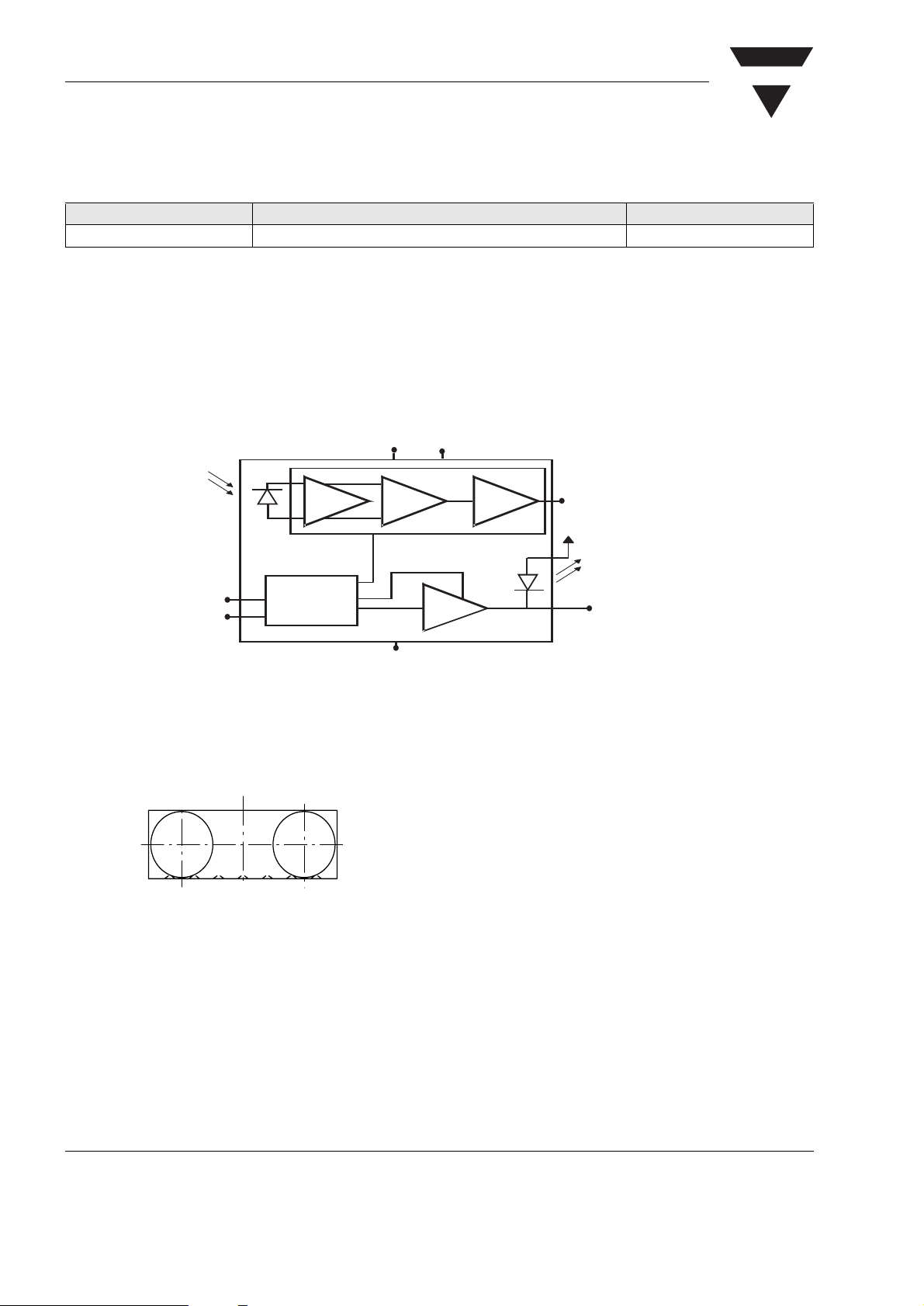
Functional Block Diagram
VISHAY
18072
Pinout
TFBS6614
weight 80 mg
SD/Mode
TxD
Amp
Mode &
Power
Control
V
CC1
Comp
GND
V
Driver
logic
Driver
V
RxD
CC2
LEDA
LEDC
18304
www.vishay.com
2
1234567
Document Number 82611
Rev. 1.4, 28-Oct-03

VISHAY
TFBS6614
Vishay Semiconductors
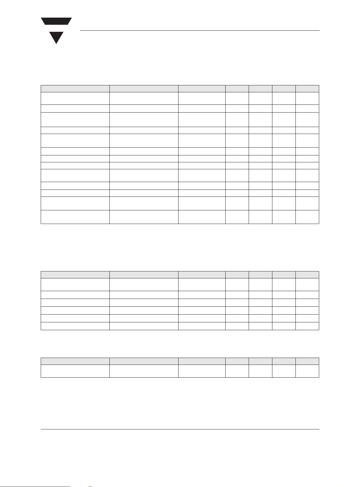
Absolute Maximum Ratings
Reference Point Ground, Pin 8, unless otherwise noted
Parameter Test Conditions Symbol Min Ty p. Max Unit
Analog Supply Voltage Range,
all states
Digital Supply Voltage Range V
Input Current During Transmit, VCC = 5.0 V,
TxD = V
DD
Output Sink Current, RxD 25.0 mA
Peak IRED Current V
Average IRED Current V
Power Dissipation 500 mW
Junction Temperature 125 °C
Ambient Temperature Range
(Operating)
Storage Temperature Range T
Soldering Temperature t = 20 s @ 215 °C 215 240 °C
Transmitter Data and Shutdown
Input Voltage
Receiver Data Output Voltage RxD - 0.5 VDD +
= 2.7 V, TxD = VDD, 125 ns
CC1
pulse
= 2.7 V 125 mA
CC2
V
CC1
DD
T
A
S
V
, V
TxD
SD
- 0.5 + 6.0 V
- 0.5 + 6.0 V
10.0 mA
650 mA
- 25 + 85 °C
- 25 + 85 °C
- 0.5 VDD +
0.5
0.5
V
V
Optoelectronic Characteristics
Receiver
TA = 25 °C, VCC = 2.7 V to 5.5 V unless othervise noted
Parameter Test Conditions Symbol Min Ty p. Max Unit
Minimum Detection Threshold
Irradiance
Analog Supply Voltage Range Specified operation V
Digital Supply Voltage Range Specified operation V
Maximum LED Anode Voltage V
ICC Shut Down Current VCC = 5 V I
ICC Idle Current VCC = 5 V I
4.0 Mbit/s,
l = 850 nm to 900 nm
Transmitter
TA = 25 °C, VCC = 2.7 V to 5.5 V unless othervise noted
Parameter Test Conditions Symbol Min Ty p. Max Unit
Output Radiant Intensity α = 0 °C, 15 °C,
TxD = High, SD = Low
E
e
CC
DD
LEDA
CC1
CC2
I
e
100
2.7 5.5 V
1.5 5.5 V
VCC + 4 V
0.01 2.0 µA
1.6 mA
110 mW/sr
mW/m
2
Document Number 82611
Rev. 1.4, 28-Oct-03
www.vishay.com
3
 Loading...