

Page 1
TFBS4650
Vishay Semiconductors
Infrared Transceiver
9.6 kbit/s to 115.2 kbit/s (SIR)
Description
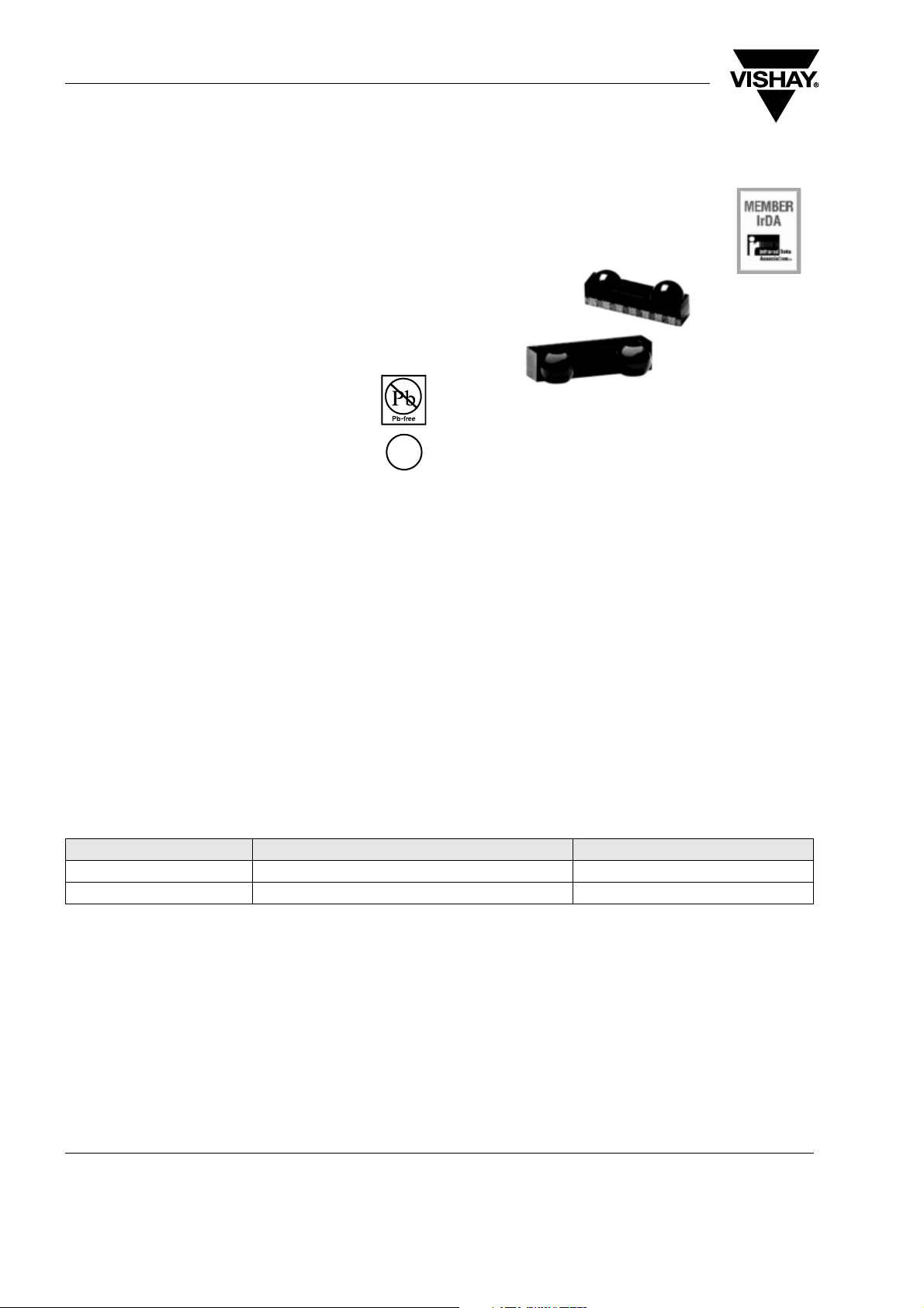
The TFBS4650 is one of the smallest IrDA® compliant
transceivers available. It supports data rates up to
115 kbit/s. The transceiver consists of a PIN photodiode, infrared emitter, and control IC in a single package.
Features
• Compliant with the IrDA physical layer
IrPHY 1.4 (low power specification,
9.6 kbit/s to 115.2 kbit/s)
• Link distance: 30 cm/20 cm full 15°
with standard or low power IrDA, respectively. Emission intensity can be set by an external
resistor to increase the range for extended low
power spec to > 50 cm
• Typical transmission distance to standard device:
50 cm
• Small package L 6.8 mm x W 2.8 mm x H 1.6 mm
• Low current consumption
75 µA idle at 3.6 V
cone
e4
20206
• Shutdown current 10 nA typical at 25 °C
• Operates from 2.4 V to 3.6 V within specification
over full temperature range from - 25 °C to + 85 °C
• Split power supply, emitter can be driven by a separate power supply not loading the regulated. U.S.
Pat. No. 6,157,476
• Lead (Pb)-free device
• Qualified for lead (Pb)-free and Sn/Pb processing
(MSL4)
• Device in accordance with RoHS 2002/95/EC and
WEEE 2002/96/EC
Applications
• Mobile phone
• PDAs
Parts Table
Part Description Qty / Reel
TFBS4650-TR1 Oriented in carrier tape for side view surface mounting 1000 pcs
TFBS4650-TR3 Oriented in carrier tape for side view surface mounting 2500 pcs
www.vishay.com
120
Document Number 84672
Rev. 1.1, 03-Jul-06
Page 2
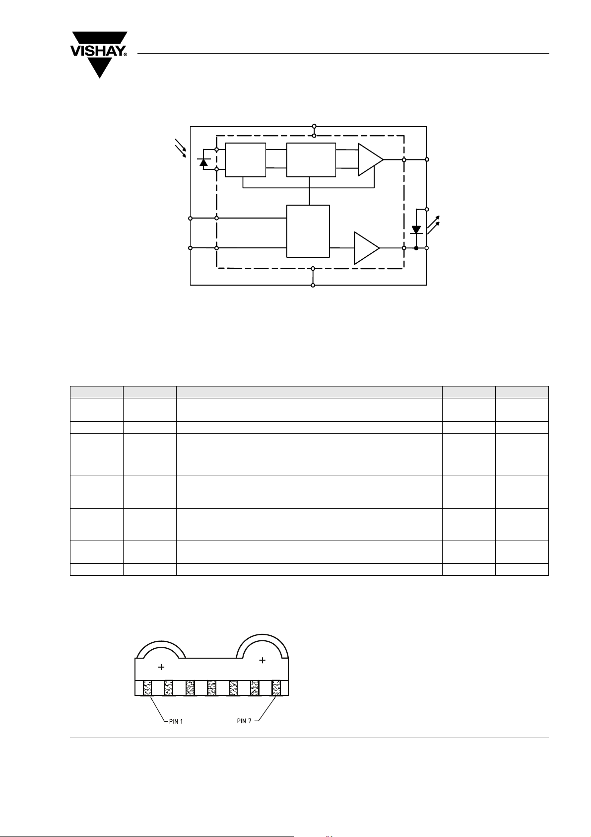
Functional Block Diagram
A
r
TFBS4650
Vishay Semiconductors
V
CC
PD
mplifie
Comparator
Tri-State
Driver
RxD
IREDA
SD
TxD
Mode
Control
IRED Driver
IRED
IREDC
ASIC
GND
19283
Pin Description
Pin Number Function Description I/O Active
1 IREDA IRED Anode, connected via a current limiting resistor to V
unregulated power supply can be used.
2 IREDC IRED Cathode, do not connect for standard operation
3 TXD Transmitter Data Input. Setting this input above the threshold turns on the
transmitter.
This input switches the IRED with the maximum transmit pulse width of
4 RXD Receiver Output. Normally high, goes low for a defined pulse duration with
the rising edge of the optical input signal. Output is a CMOS tri-state driver,
which swings between ground and V
5 SD Shut Down. Logic Low at this input enables the receiver, enables the
transmitter, and un-tri-states the receiver output. It must be driven high for
shutting down the transceiver.
6V
7 GND Ground
CC
Power Supply, 2.4 V to 3.6 V. This pin provides power for the receiver and
transmitter drive section. Connect V
about 50 µs.
. Receiver echoes transmitter output.
cc
via an optional filter.
CC1
. A separate
CC2
IHIGH
OLOW
IHIGH
Pinout
TFBS4650, bottom view
weight 0.05 g
19284
Document Number 84672
Rev. 1.1, 03-Jul-06
www.vishay.com
121
Page 3

TFBS4650
Vishay Semiconductors
Absolute Maximum Ratings
Reference point Pin, GND unless otherwise noted.
Typical values are for DESIGN AID ONLY, not guaranteed nor subject to production testing.
Parameter Test Conditions Symbol Min Ty p. Max Unit
Supply voltage range,
0 V < V
transceiver
Supply voltage range,
0 V < V
transmitter
Voltage at RXD All states V
Input voltage range, transmitter
Independent of V
TXD
< 6 V V
CC2
< 3.6 V V
CC1
or V
CC1
CC2
CC1
CC2
V
in
in
Input currents For all pins, except IRED anode
pin
Output sinking current 20 mA
Power dissipation P
Junction temperature T
Ambient temperature range
(operating)
Storage temperature range T
D
J
T
amb
stg
Soldering temperature ***) see section Recommended
Solder Profile
Repetitive pulse output current < 90 µs, t
Average output current
< 20 % I
on
(RP) 500 mA
IRED
I
(DC) 100 mA
IRED
(transmitter)
Virtual source size Method: (1-1/e) encircled
d0.8 mm
energy
Maximum Intensity for Class 1 IEC60825-1 or
EN60825-1,
I
e
edition Jan. 2001
*)
Due to the internal limitation measures the device is a "class1" device.
**)
IrDA specifies the max. intensity with 500 mW/sr
***)
Sn/Pb-free soldering. The product passed VISHAY’s standard convection reflow profile soldering test.
- 0.5 6.0 V
- 0.5 6.0 V
- 0.5 VCC + 0.5 V
- 0.5 6.0 V
- 40 40 mA
250 mW
125 °C
- 25 + 85 °C
- 40 + 100 °C
*)
(500)
mW/sr
**)
°C
Definitions:
In the Vishay transceiver data sheets the following nomenclature is used for defining the IrDA operating modes:
SIR: 2.4 kbit/s to 115.2 kbit/s, equivalent to the basic serial infrared standard with the physical layer version IrPhY 1.0
MIR: 576 kbit/s to 1152 kbit/s
FIR: 4 Mbit/s
VFIR: 16 Mbit/s
MIR and FIR were implemented with IrPhY 1.1, followed by IrPhY 1.2, adding the SIR Low Power Standard. IrPhY 1.3 extended the Low
Power Option to MIR and FIR and VFIR was added with IrPhY 1.4. A new version of the standard in any case obsoletes the former version.
www.vishay.com
122
Document Number 84672
Rev. 1.1, 03-Jul-06
Page 4

Electrical Characteristics
Transceiver
T
= 25 °C, VCC = 2.4 V to 3.6 V unless otherwise noted.
amb
Typical values are for DESIGN AID ONLY, not guaranteed nor subject to production testing.
Parameter Test Conditions Symbol Min Ty p . Max Unit
Supply voltage range V
Dynamic supply current
Idle, dark ambient SD = Low (< 0.8 V),
E
= 0 klx,
eamb
< 4 mW/m
E
e
2
- 25 °C ≤ T ≤ + 85 °C
Idle, dark ambient SD = Low (< 0.8 V),
= 0 klx,
E
eamb
E
< 4 mW/m
e
2
T = + 25 °C
Peak supply current during
SD = Low, TXD = High I
transmission
Shutdown supply current
dark ambient
SD = High
(> V
- 0.5 V),
CC
T = 25 °C, Ee = 0 klx
Shutdown supply current, dark
ambient
SD = High
(> V
- 0.5 V),
CC
- 25 °C ≤ T ≤ + 85 °C
Operating temperature range T
Input voltage low (TXD, SD) V
Input voltage high V
Input voltage threshold SD V
Output voltage low V
= 2.4 V to 3.6 V V
CC
= 2.4 V to 3.6 V 0.9 1.35 1.8 V
CC
= 2.4 V to 3.6 V
CC
CLOAD = 15 pF
Output voltage high V
RXD to V
pull-up impedance SD = VCC
CC
= 2.4 V to 3.6 V
CC
= 15 pF
C
LOAD
= 2.4 V to 5 V
V
CC
R
Input capacitance
(TXD, SD)
I
CC
I
CC
ccpk
I
SD
I
SD
V
V
RXD
C
CC
A
IL
IH
OL
OH
I
2.4 3.6 V
- 25 + 85 °C
- 0.5 0.5 V
VCC - 0.5 6.0 V
- 0.5 V
V
CC
TFBS4650
Vishay Semiconductors
90 130 µA
75 µA
23mA
0.1 µA
1.0 µA
x 0.15 V
CC
x 0.8 V
500 kΩ
+ 0.5 V
CC
6pF
Document Number 84672
Rev. 1.1, 03-Jul-06
www.vishay.com
123
Page 5

TFBS4650
Vishay Semiconductors
Optoelectronic Characteristics
Receiver
T
= 25 °C, VCC = 2.4 V to 3.6 V unless otherwise noted.
amb
Typical values are for DESIGN AID ONLY, not guaranteed nor subject to production testing.
Parameter Test Conditions Symbol Min Ty p. Max Unit
Sensitivity:
Minimum irradiance Ee in
9.6 kbit/s to 115.2 kbit/s
λ = 850 nm to 900 nm
E
e
40
(4.0)
81
(8.1)
angular range *)**)
Maximum irradiance Ee in
angular range ***)
No receiver output input
irradiance
λ = 850 nm to 900 nm E
According to IrDA IrPHY 1.4,
Appendix A1, fluorescent light
e
E
e
5
(500)
4
(0.4)
specification
Rise time of output signal 10 % to 90 %, C
Fall time of output signal 90 % to 10 %, C
RXD pulse width of output
signal, 50%****)
Input pulse width
1.63 µs
= 15 pF t
L
= 15 pF t
L
r (RXD)
f (RXD)
t
PW
20 100 ns
20 100 ns
1.7 2.0 2.9 µs
Receiver start up time Power on delay 100 150 µs
Latency t
*)
This parameter reflects the backlight test of the IrDA physical layer specification to guarantee immunity against light from fluorescent
L
50 200 µs
lamps
**)
IrDA sensitivity definition: Minimum Irradiance Ee In Angular Range, power per unit area. The receiver must meet the BER specification
while the source is operating at the minimum intensity in angular range into the minimum half-angle range at the maximum Link Length
***)
Maximum Irradiance Ee In Angular Range, power per unit area. The optical delivered to the detector by a source operating at the maximum intensity in angular range at Minimum Link Length must not cause receiver overdrive distortion and possible related link errors. If
placed at the Active Output Interface reference plane of the transmitter, the receiver must meet its bit error ratio (BER) specification.
****)
RXD output is edge triggered by the rising edge of the optical input signal. The output pulse duration is independent of the input pulse
duration.
mW/m
(µW/cm
kW/m
(mW/cm
mW/m
(µW/cm
2
2
)
2
2
2
2
)
)
For more definitions see the document “Symbols and Terminology” on the Vishay Website (http://www.vishay.com/docs/82512/82512.pdf).
www.vishay.com
124
Document Number 84672
Rev. 1.1, 03-Jul-06
Page 6
Transmitter
T
= 25 °C, VCC = 2.4 V to 3.6 V unless otherwise noted.
amb
Typical values are for DESIGN AID ONLY, not guaranteed nor subject to production testing.
Parameter Test Conditions Symbol Min Ty p. Max Unit
IRED operating current, current
controlled
The IRED current is internally
controlled but also can be
reduced by an external resistor
R1
Output leakage IRED current Tamb = 85°C I
Output radiant intensity *) α = 0°, 15°, TXD = High, SD =
Low, V
= 3.0 V, V
CC1
CC2
= 3.0 V,
R1 = 30 Ω (resulting in about
50 mA drive current)
Output radiant intensity *) α = 0°, 15°, TXD = High, SD =
Low, V
= 3.0 V, V
CC1
CC2
= 3.0 V,
R1 = 0 Ω, If = 300 mA
Output radiant intensity *) V
= 5.0 V, α = 0°, 15°
CC1
TXD = Low or SD = High
(Receiver is inactive as long as
SD = High)
Saturation voltage of IRED
driver
V
= 3.0 V, If = 50 mA V
CC
Peak - emission wavelength λ
Optical rise time,
Optical fall time
Optical output pulse duration Input pulse width t < 30 µs
Input pulse width t ≥ 30 µs
Optical output pulse duration Input pulse width t = 1.63 µs t
I
D
IRED
I
e
I
e
I
e
CEsat
p
t
ropt
t
fopt
t
opt
t
opt
opt
,
TFBS4650
Vishay Semiconductors
200 400 mA
1µA
4 150 mW/sr
25 mW/sr
0.04 mW/sr
0.4 V
880 886 900 nm
20 100 ns
t
30
50 300
1.45 1.61 2.2 µs
µs
µs
Optical overshoot 20 %
*)
The radiant intensity can be adjusted by the external current limiting resistor to adapt the intensity to the desired value. The given value
is for minimum current consumption. This transceiver can be adapted to > 50 cm operation by increasing the current to > 200 mA, e.g.
operating the transceiver without current control resistor (i.e. R1 = 0 Ω) and using the internal current control.
Table 1.
Truth table
Inputs Outputs
SD TXD
Optical input Irradiance mW/m
high x x Tri-state floating with a weak
low high x low (echo on) I
low high > 50 µs x high 0
low low < 4 high 0
low low > Min. irradiance E
< Max. irradiance E
low low > Max. irradiance E
2
RXD Transmitter
0
pull-up to the supply voltage
e
e
e
e
low (active) 0
x0
Document Number 84672
Rev. 1.1, 03-Jul-06
www.vishay.com
125
Page 7

TFBS4650
Vishay Semiconductors
Recommended Circuit Diagram
Operated at a clean low impedance power supply the
TFBS4650 needs only one additional external component when the IRED drive current should be minimized for minimum current consumption according
the low power IrDA standard. When combined operation in IrDA and Remote Control is intended no current limiting resistor is recommended.
However, depending on the entire system design and
board layout, additional components may be required
(see figure 1). When long wires are used for bench
tests, the capacitors are mandatory for testing rise/fall
time correctly.
V
CC2
V
CC1
GND
SD
Txd
Rxd
Figure 1. Recommended Application Circuit
C1
R1
R2
The capacitor C1 is buffering the supply voltage V
and eliminates the inductance of the power supply
line. This one should be a small ceramic version or
other fast capacitor to guarantee the fast rise time of
the IRED current. The resistor R1 is necessary for
controlling the IRED drive current when the internally
controlled current is too high for the application.
Vishay transceivers integrate a sensitive receiver and
a built-in power driver. The combination of both needs
a careful circuit board layout. The use of thin, long,
resistive and inductive wiring should be avoided. The
inputs (TXD, SD) and the output RXD should be
directly (DC) coupled to the I/O circuit.
The capacitor C2 combined with the resistor R2 is the
low pass filter for smoothing the supply voltage.
As already stated above R2, C1 and C2 are optional
and depend on the quality of the supply voltages V
and injected noise. An unstable power supply with
dropping voltage during transmission may reduce the
sensitivity (and transmission range) of the transceiver.
The placement of these parts is critical. It is strongly
C2
IRED Anode
IRED Cathode
V
CC
Ground
SD
Txd
Rxd
19286
cc2
CCx
recommended to position C2 as close as possible to
the transceiver power supply pins.
When connecting the described circuit to the power
supply, low impedance wiring should be used.
In case of extended wiring the inductance of the
power supply can cause dynamically a voltage drop
at V
. Often some power supplies are not able to
CC2
follow the fast current is rise time. In that case another
10 µF cap at V
will be helpful.
CC2
Keep in mind that basic RF-design rules for circuit
design should be taken into account. Especially
longer signal lines should not be used without termination. See e.g. "The Art of Electronics" Paul Horowitz,
Wienfield Hill, 1989, Cambridge University Press,
ISBN: 0521370957.
Table 2.
Recommended Application Circuit Components
Component Recommended Value
C1, C2 0.1 µF, Ceramic Vishay part#
VJ 1206 Y 104 J XXMT
R1 See table 3
R2 47 Ω, 0.125 W (V
CC1
= 3 V)
Table 3.
Recommended resistor R1 [Ω]
V
CC2
[V]
2.7 24
3.0 30
3.3 36
Minimized current consumption,
IrDA Low power compliant
www.vishay.com
126
Document Number 84672
Rev. 1.1, 03-Jul-06
Page 8

Recommended Solder Profiles
0
20
40
60
80
100
120
140
160
180
200
220
240
260
0 50 100 150 200 250 300 350
Time/s
Tem peratu re/°C
2...4 °C/s
2...4 °C/s
10 s max. at 230 °C
120 s...180 s
160 °C max.
240 °C max.
90 s max.
20
Solder Profile for Sn/Pb soldering
Figure 2. Recommended Solder Profile for Sn/Pb soldering
19431
TFBS4650
Vishay Semiconductors
Manual Soldering
Manual soldering is the standard method for lab use.
However, for a production process it cannot be recommended because the risk of damage is highly
dependent on the experience of the operator. Nevertheless, we added a chapter to the above mentioned
application note, describing manual soldering and
desoldering.
Storage
The storage and drying processes for all VISHAY
transceivers (TFDUxxxx and TFBSxxx) are equivalent to MSL4.
The data for the drying procedure is given on labels
on the packing and also in the application note
"Taping, Labeling, Storage and Packing"
(http://www.vishay.com/docs/82601/82601.pdf).
Lead (Pb)-Free, Recommended Solder Profile
The TFBS4650 is a lead (Pb)-free transceiver and
qualified for lead (Pb)-free processing. For lead
(Pb)-free solder paste like Sn(3.0-4.0)Ag(0.5-0.9)Cu,
there are two standard reflow profiles: Ramp-SoakSpike (RSS) and Ramp-To-Spike (RTS). The RampSoak-Spike profile was developed primarily for reflow
ovens heated by infrared radiation. With widespread
use of forced convection reflow ovens the Ramp-ToSpike profile is used increasingly. Shown below in figure 3 is VISHAY's recommended profiles for use with
the TFBS4650 transceivers. For more details please
refer to Application note: SMD Assembly Instruction.
Wave Soldering
For TFDUxxxx and TFBSxxxx transceiver devices
wave soldering is not recommended.
280
260
240
220
200
180
160
140
120
Temperature/°C
100
80
60
2 °C...4 °C/s
40
20
0
0 50 100 150 200 250 300 350
19261
T ≥ 255 °C for 20 s max
T ≥ 217 °C for 50 s max
90 s...120 s
Time/s
s
50 s max.
T
peak
= 260 °C max.
Figure 3. Solder Profile, RSS Recommendation
2 °C...4 °C/s
Document Number 84672
Rev. 1.1, 03-Jul-06
www.vishay.com
127
Page 9

TFBS4650
Vishay Semiconductors
Package Dimensions
www.vishay.com
128
19322
Figure 4. TFBS4650 mechanical dimensions, tolerance ± 0.2 mm, if not otherwise mentioned
19729
Figure 5. TFBS4650 soldering footprint, tolerance ± 0.2 mm, if not otherwise mentioned
Document Number 84672
Rev. 1.1, 03-Jul-06
Page 10

Reel Dimensions
TFBS4650
Vishay Semiconductors
Drawing-No.: 9.800-5090.01-4
Issue: 1; 29.11.05
14017
Tape Width A max. N W1 min. W2 max. W3 min. W3 max.
mm mm mm mm mm mm mm
16 330 50 16.4 22.4 15.9 19.4
Document Number 84672
Rev. 1.1, 03-Jul-06
www.vishay.com
129
Page 11

TFBS4650
Vishay Semiconductors
Tape Dimensions in mm
www.vishay.com
130
19783
Document Number 84672
Rev. 1.1, 03-Jul-06
Page 12

TFBS4650
Vishay Semiconductors
Ozone Depleting Substances Policy Statement
It is the policy of Vishay Semiconductor GmbH to
1. Meet all present and future national and international statutory requirements.
2. Regularly and continuously improve the performance of our products, processes, distribution and operating
systems with respect to their impact on the health and safety of our employees and the public, as well as
their impact on the environment.
It is particular concern to control or eliminate releases of those substances into the atmosphere which are
known as ozone depleting substances (ODSs).
The Montreal Protocol (1987) and its London Amendments (1990) intend to severely restrict the use of ODSs
and forbid their use within the next ten years. Various national and international initiatives are pressing for an
earlier ban on these substances.
Vishay Semiconductor GmbH has been able to use its policy of continuous improvements to eliminate the use
of ODSs listed in the following documents.
1. Annex A, B and list of transitional substances of the Montreal Protocol and the London Amendments
respectively
2. Class I and II ozone depleting substances in the Clean Air Act Amendments of 1990 by the Environmental
Protection Agency (EPA) in the USA
3. Council Decision 88/540/EEC and 91/690/EEC Annex A, B and C (transitional substances) respectively.
Vishay Semiconductor GmbH can certify that our semiconductors are not manufactured with ozone depleting
substances and do not contain such substances.
We reserve the right to make changes to improve technical design
and may do so without further notice.
Parameters can vary in different applications. All operating parameters must be validated for each
customer application by the customer. Should the buyer use Vishay Semiconductors products for any
unintended or unauthorized application, the buyer shall indemnify Vishay Semiconductors against all
claims, costs, damages, and expenses, arising out of, directly or indirectly, any claim of personal
damage, injury or death associated with such unintended or unauthorized use.
Vishay Semiconductor GmbH, P.O.B. 3535, D-74025 Heilbronn, Germany
www.vishay.com
131
Document Number 84672
Rev. 1.1, 03-Jul-06
Page 13

Legal Disclaimer Notice
Vishay
Document Number: 91000 www.vishay.com
Revision: 08-Apr-05 1
Notice
Specifications of the products displayed herein are subject to change without notice. Vishay Intertechnology, Inc.,
or anyone on its behalf, assumes no responsibility or liability for any errors or inaccuracies.
Information contained herein is intended to provide a product description only. No license, express or implied, by
estoppel or otherwise, to any intellectual property rights is granted by this document. Except as provided in Vishay's
terms and conditions of sale for such products, Vishay assumes no liability whatsoever, and disclaims any express
or implied warranty, relating to sale and/or use of Vishay products including liability or warranties relating to fitness
for a particular purpose, merchantability, or infringement of any patent, copyright, or other intellectual property right.
The products shown herein are not designed for use in medical, life-saving, or life-sustaining applications.
Customers using or selling these products for use in such applications do so at their own risk and agree to fully
indemnify Vishay for any damages resulting from such improper use or sale.
 Loading...