

Silicon Phototransistor in 0805 Package
20043
DESCRIPTION
TEMT7000X01 is a high speed silicon NPN epitaxial planar
phototransistor in a miniature 0805 package for surface
mounting on printed boards. The device is sensitive to visible
and near infrared radiation.
TEMT7000X01
Vishay Semiconductors
FEATURES
• Package type: surface mount
• Package form: 0805
• Dimensions (L x W x H in mm): 2 x 1.25 x 0.85
• AEC-Q101 qualified
• High photo sensitivity
• High radiant sensitivity
• Suitable for visible and near infrared radiation
• Fast response times
• Angle of half sensitivity: ϕ = ± 60°
• Package matched with IR emitter series VSMB1940X01
• Floor life: 168 h, MSL 3, acc. J-STD-020
• Lead (Pb)-free reflow soldering
• Compliant to RoHS directive 2002/95/EC and in
accordance to WEEE 2002/96/EC
• Find out more about Vishay’s Automotive Grade Product
requirements at: www.vishay.com/applications
APPLICATIONS
• Detector in automotive applications
• Light sensors
• Radiation sensors
PRODUCT SUMMARY
COMPONENT I
TEMT7000X01 225 to 675 ± 60 470 to 1090
Note
Test condition see table “Basic Characteristics”
(µA) ϕ (deg) λ
caE
0.1
(nm)
ORDERING INFORMATION
ORDERING CODE PACKAGING REMARKS PACKAGE FORM
TEMT7000X01 Tape and reel MOQ: 3000 pcs, 3000 pcs/reel 0805
Note
MOQ: minimum order quantity
ABSOLUTE MAXIMUM RATINGS
PARAMETER TEST CONDITION SYMBOL VALUE UNIT
Collector emitter voltage V
Emitter collector voltage V
Collector current I
Power power dissipation T
Junction temperature T
Operating temperature range T
Storage temperature range T
Soldering temperature Acc. reflow profile fig. 7 T
Thermal resistance junction/ambient Acc. J-STD-051 R
Note
T
= 25 °C, unless otherwise specified
amb
≤ 55 °C P
amb
CEO
ECO
C
V
j
amb
stg
sd
thJA
20 V
7V
20 mA
100 mW
100 °C
- 40 to + 100 °C
- 40 to + 100 °C
260 °C
270 K/W
Document Number: 81961 For technical questions, contact: detectortechsupport@vishay.com
Rev. 1.0, 12-May-09 1
www.vishay.com
TEMT7000X01
Vishay Semiconductors
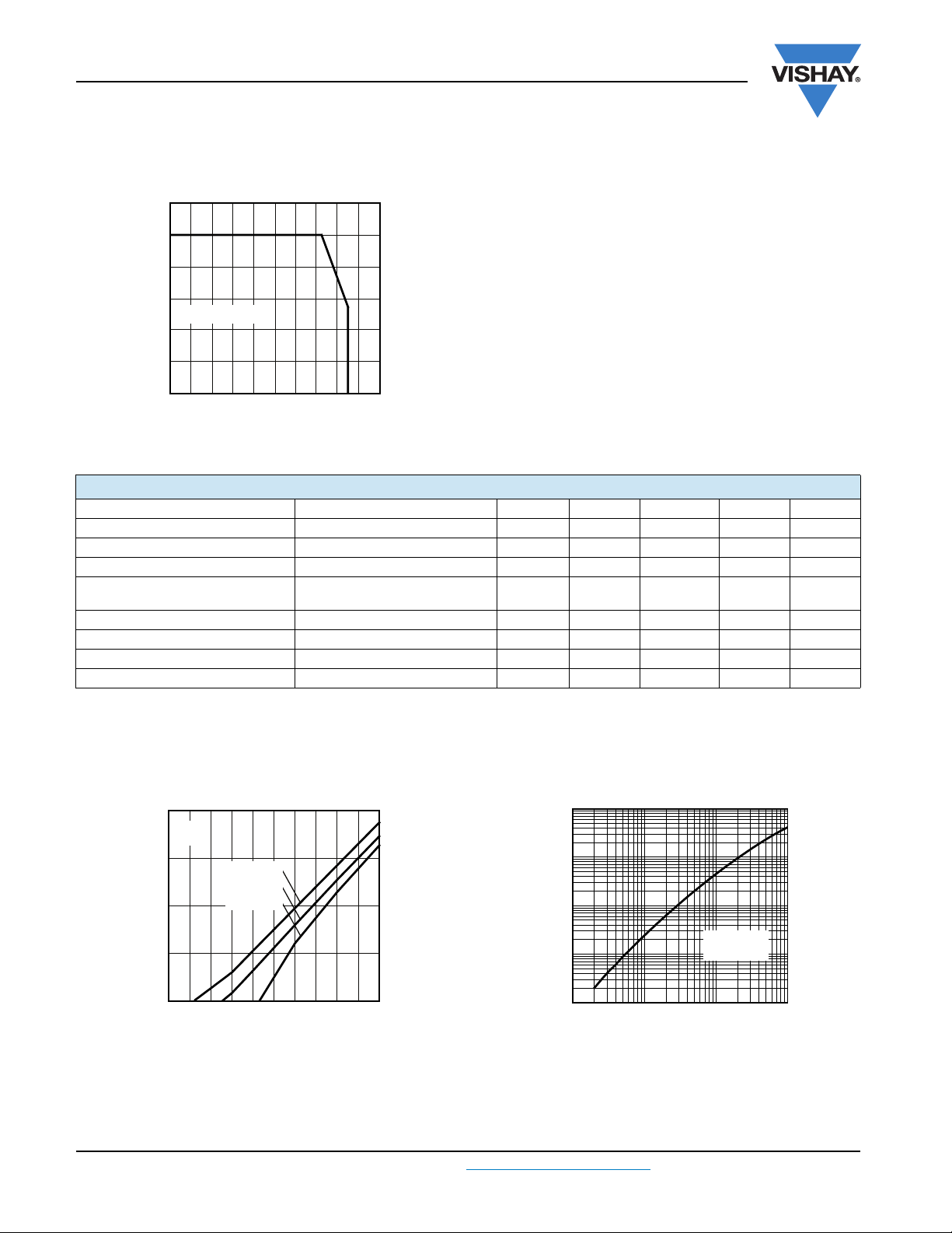
120
100
80
60
R
= 270 K/W
thJA
40
- Power Dissipation (mW)
V
20
P
0
0 10203040 50607080 90 100
21331
T
- Ambient Temperature (°C)
amb
Silicon Phototransistor in 0805 Package
Fig. 1 - Power Dissipation Limit vs. Ambient Temperature
BASIC CHARACTERISTICS
PARAMETER TEST CONDITION SYMBOL MIN. TYP. MAX. UNIT
Collector emitter breakdown voltage I
Collector dark current V
Collector emitter capacitance V
E
Collector light current
e
Angle of half sensitivity ϕ ± 60 deg
Wavelength of peak sensitivity λ
Range of spectral bandwidth λ
Collector emitter saturation voltage I
Note
= 25 °C, unless otherwise specified
T
amb
= 0.1 mA V
C
= 5 V, E = 0 I
CE
= 0 V, f = 1 MHz, E = 0 C
CE
= 1 mW/cm2, λ = 950 nm,
V
= 5 V
CE
= 0.05 mA V
C
CEO
CEO
CEO
I
CA
p
0.1
CEsat
20 V
1 100 nA
25 pF
225 450 675 µA
850 nm
470 to 1090 nm
0.4 V
BASIC CHARACTERISTICS
T
= 25 °C, unless otherwise specified
amb
10 000
IF = 0
1000
100
10
VCE = 70 V
V
= 25 V
CE
V
= 5 V
CE
- Collector Dark Current (nA)
CE0
I
1
0 1020304050607080 90 100
20594
- Ambient Temperature (°C)
T
amb
Fig. 2 - Collector Dark Current vs. Ambient Temperature Fig. 3 - Collector Light Current vs. Irradiance
www.vishay.com For technical questions, contact: detectortechsupport@vishay.com
2 Rev. 1.0, 12-May-09
10
1
0.1
0.01
- Collector Light Current (mA)
ca
I
0.001
0.01 0.1 1 10
21551
Ee - Irradiance (mW/cm²)
VCE = 5 V
Document Number: 81961
TEMT7000X01
Silicon Phototransistor in 0805 Package
100
90
80
70
60
50
40
30
- Rise/Fall Time (µs)
f
t
/t
t
20599
r
r
20
10
0
0 250 500 750 1000 1250 1500 1750 2000
Fig. 4 - Rise/Fall Time vs. Collector Current
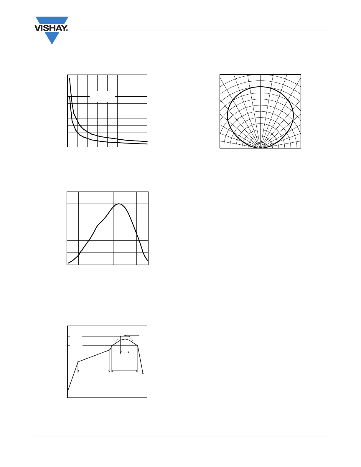
1.2
1.0
RL = 100 Ω
t
f
- Collector Current (µA)
I
C
Vishay Semiconductors
0°
10° 20°
1.0
0.9
0.8
- Relative Radiant Intensity
e rel
0.7
I
0.4 0.2 0
0.6
94 8013
Fig. 6 - Relative Radiant Sensitivity vs. Angular Displacement
30°
40°
50°
60°
70°
80°
ϕ - Angular Displacement
0.8
0.6
0.4
- Relative Spectral Sensitivity
rel
0.2
S (λ)
0
400 500 600 700 800 900 1000 1100
21555
λ - Wavelength (nm)
Fig. 5 - Relative Spectral Sensitivity vs. Wavelength
REFLOW SOLDER PROFILE
300
255 °C
250
240 °C
217 °C
200
150
100
max. 120 s
Temperature (°C)
50
max. ramp up 3 °C/s
0
0 50 100 150 200 250 300
19841
max. ramp down 6 °C/s
Time (s)
Fig. 7 - Lead (Pb)-free Reflow Solder Profile acc. J-STD-020D
max. 260 °C
245 °C
max. 30 s
max. 100 s
DRYPACK
Devices are packed in moisture barrier bags (MBB) to
prevent the products from moisture absorption during
transportation and storage. Each bag contains a desiccant.
FLOOR LIFE
Floor life (time between soldering and removing from MBB)
must not exceed the time indicated on MBB label:
Floor life: 168 h
Conditions: T
< 30 °C, RH < 60 %
amb
Moisture sensitivity level 3, acc. to J-STD-020.
DRYING
In case of moisture absorption devices should be baked
before soldering. Conditions see J-STD-020 or label.
Devices taped on reel dry using recommended conditions
192 h at 40 °C (+ 5 °C), RH < 5 %.
Document Number: 81961 For technical questions, contact: detectortechsupport@vishay.com
www.vishay.com
Rev. 1.0, 12-May-09 3

TEMT7000X01
Vishay Semiconductors
PACKAGE DIMENSIONS in millimeters
Silicon Phototransistor in 0805 Package
19757
www.vishay.com For technical questions, contact: detectortechsupport@vishay.com
4 Rev. 1.0, 12-May-09
Document Number: 81961

TEMT7000X01
Silicon Phototransistor in 0805 Package
BLISTER TAPE DIMENSIONS in millimeters
Vishay Semiconductors
20690
Quantity per reel: 3000 pcs
Document Number: 81961 For technical questions, contact: detectortechsupport@vishay.com
Rev. 1.0, 12-May-09 5
www.vishay.com

TEMT7000X01
Vishay Semiconductors
REEL DIMENSIONS in millimeters
Silicon Phototransistor in 0805 Package
20875
www.vishay.com For technical questions, contact: detectortechsupport@vishay.com
6 Rev. 1.0, 12-May-09
Document Number: 81961

Legal Disclaimer Notice
Vishay
Disclaimer
All product specifications and data are subject to change without notice.
Vishay Intertechnology, Inc., its affiliates, agents, and employees, and all persons acting on its or their behalf
(collectively, “Vishay”), disclaim any and all liability for any errors, inaccuracies or incompleteness contained herein
or in any other disclosure relating to any product.
Vishay disclaims any and all liability arising out of the use or application of any product described herein or of any
information provided herein to the maximum extent permitted by law. The product specifications do not expand or
otherwise modify Vishay’s terms and conditions of purchase, including but not limited to the warranty expressed
therein, which apply to these products.
No license, express or implied, by estoppel or otherwise, to any intellectual property rights is granted by this
document or by any conduct of Vishay.
The products shown herein are not designed for use in medical, life-saving, or life-sustaining applications unless
otherwise expressly indicated. Customers using or selling Vishay products not expressly indicated for use in such
applications do so entirely at their own risk and agree to fully indemnify Vishay for any damages arising or resulting
from such use or sale. Please contact authorized Vishay personnel to obtain written terms and conditions regarding
products designed for such applications.
Product names and markings noted herein may be trademarks of their respective owners.
Document Number: 91000 www.vishay.com
Revision: 18-Jul-08 1
 Loading...