


VISHAY
Silicon Phototransistor
TEMT1000/1020/1030/1040
Vishay Semiconductors
Description
TEMT1000 series are high speed and high sensitive
silicon NPN epitaxial planar phototransistors in SMD
package with dome lens. Due to integrated Daylight
filter devices are sensitive for IR radiation only.
TEMT1000
TEMT1030
Features
• High photo sensitivity
• Fast response times
• Angle of half sensitivity ϕ = ± 15°
• Daylight filter matched to IR Emitters
(λ = 870 nm to 950 nm)
• Versatile terminal configurations
• Matched IR Emitter series: TSML1000
IR Detector for Daylight application
Photo interrupters
Applications
Detector in electronic control and drive circuits
Counter
Encoder
Absolute Maximum Ratings
T
= 25 °C, unless otherwise specified
amb
Parameter Te s t co n di ti o n Symbol Value Unit
Emitter Collector Voltage V
Collector Current I
Peak Collector Current tp/T = 0.5, tp ≤ 10 ms I
Total Power Dissipation T
Junction Temperature T
Storage Temperature Range T
Operating Temperature Range T
Soldering Temperature t ≤ 5 s T
Thermal Resistance Junction/Ambient R
≤ 55 °C P
amb
ECO
C
CM
tot
stg
amb
sd
thJA
TEMT1020
TEMT1040
100 mA
100 mW
j
100 °C
- 40 to + 100 °C
- 40 to + 85 °C
<260 °C
400 K/W
16757
5 V
50 mA
Basic Characteristics
T
= 25 °C, unless otherwise specified
amb
Paramete r Test c o n d ition Symbol Min Typ . Max Unit
Collector Emitter Voltage IC = 1 mA V
Collector Dark Current VCE = 20 V, E = 0 I
Collector Emitter Capacitance VCE = 5 V, f = 1 MHz, E=0 C
Angle of Half Sensitivity ϕ ±15 deg
Wavelength of Peak Sensitivity λ
Range of Spectral Bandwidth λ
Collector Emitter Saturation
Vo ltage
Tur n - O n T i m e VS = 5 V, IC = 5 mA,
Document Number 81554
Rev. 5, 21-May-03
Ee = 1 mW/cm2,
λ = 950 nm, I
R
= 100 Ω
L
= 0.1 mA
C
V
CEO
CEO
CEO
p
0.5
CEsat
t
on
70 V
1 200 nA
3 pF
950 nm
750 to 980 nm
0.3 V
2.0 µs
www.vishay.com
1

TEMT1000/1020/1030/1040
Vishay Semiconductors
Paramete r Test condition Symbol Min Typ . Max Unit
Turn-Off Time VS = 5 V, IC = 5 mA,
R
= 100 Ω
L
Cut-Off Frequency VS = 5 V, IC = 5 mA,
R
= 100 Ω
L
Collector Light Current
Ee = 1 mW/cm2,
λ = 950 nm, V
CE
= 5V
VISHAY
t
off
f
c
I
ca
2 7.0 mA
2.3 µs
180 kHz
Typical Characteristics (T
4
10
3
10
VCE=20V
40 60 80
- Ambient Temperature ( ° C)
amb
CEO
I - Collector Dark Current ( nA )
94 8304
10
10
10
2
1
0
20
T
= 25 °C unless otherwise specified)
amb
100
Figure 1. Collector Dark Current vs. Ambient Temperature
2.0
1.8
ca rel
I - Relative Collector Current
94 8239
1.6
1.4
1.2
1.0
0.8
0.6
VCE=5V
= 1 mW/cm
E
e
ı = 950 nm
λ
0
20 40 60 80
T
amb
2
100
- Ambient Temperature ( ° C)
10
8
6
4
2
0
CEO
C - Collector Emitter Capacitance ( pF )
0.1 1 1 0
V
94 8294
- Collector Emitter Voltage ( V )
CE
f=1MHz
100
Figure 3. Collector Emitter Capacitance vs. Collector Emitter
Voltage
8
VCE=5V
R
= 100
L
= 950 nm
λ
Ω
t
off
t
on
t /t - Turn on / Turn off Time ( µ s)
94 8293
6
4
2
off
on
0
2046 1412108
IC- Collector Current ( mA )
Figure 2. Relative Collector Current vs. Ambient Temperature
www.vishay.com
2
Figure 4. Turn On/Turn Off Time vs. Collector Current
Document Number 81554
Rev. 5, 21-May-03

VISHAY
TEMT1000/1020/1030/1040
Vishay Semiconductors
°
0
10°20
1.0
0.9
0.8
rel
S - Relative Sensitivity
0.7
0.4 0.2 0 0.2 0.4
0.6
94 8248
Figure 5. Relative Radiant Sensitivity vs. Angular Displacement
°
30°
40°
50°
60°
70°
80°
0.6
Document Number 81554
Rev. 5, 21-May-03
www.vishay.com
3

TEMT1000/1020/1030/1040
Vishay Semiconductors
Package Dimensions in mm
TEMT1000
VISHAY
Package Dimensions in mm
TEMT1020
16104
www.vishay.com
4
16105
Document Number 81554
Rev. 5, 21-May-03

VISHAY
Package Dimensions in mm
TEMT1030
TEMT1000/1020/1030/1040
Vishay Semiconductors
Package Dimensions in mm
TEMT1040
16756
16500
Document Number 81554
Rev. 5, 21-May-03
www.vishay.com
5
TEMT1000/1020/1030/1040
Vishay Semiconductors
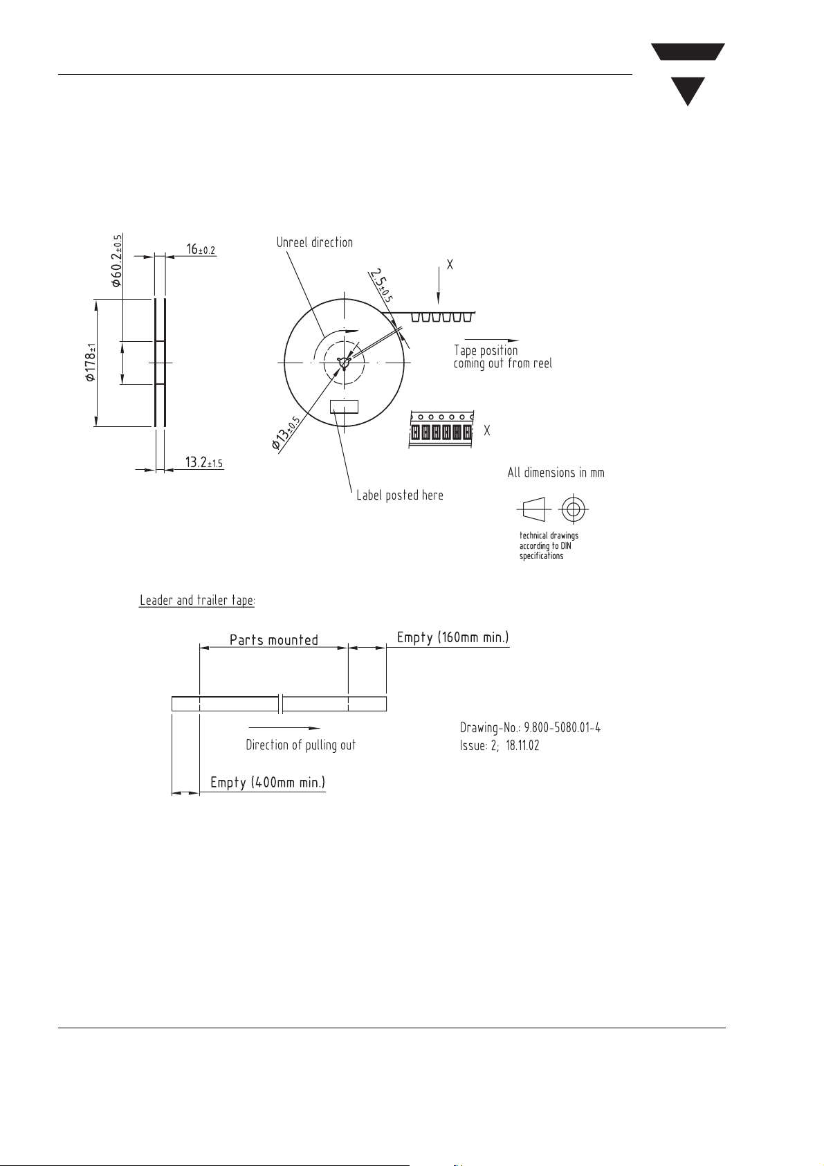
Reel Dimensions
VISHAY
www.vishay.com
6
18033
Document Number 81554
Rev. 5, 21-May-03

VISHAY
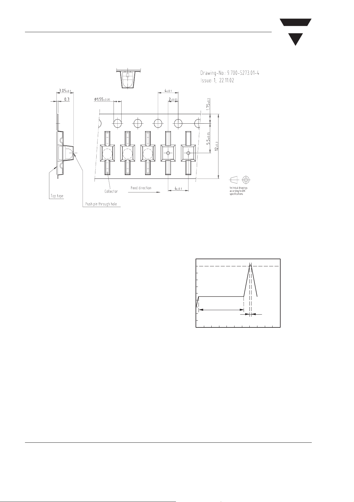
Taping TEMT1000
TEMT1000/1020/1030/1040
Vishay Semiconductors
Taping TEMT1020
18089
Document Number 81554
Rev. 5, 21-May-03
18090
www.vishay.com
7
TEMT1000/1020/1030/1040
Vishay Semiconductors
Taping TEMT1030
VISHAY
Precautions For Use
1. Over-current-proof
Customer must apply resistors for protection, otherwise slight voltage shift will cause big current change
(Burn out will happen).
2. Storage
2.1 Storage temperature and rel. humidity conditions
are: 5°C to 35°C, R.H. 60%
2.2 Floor life must not exceed 168 h, acc. to JEDEC
level 3, J-STD-020.
Once the package is opened, the products should be
used within a week. Otherwise, they should be kept in
a damp proof box with desiccant.
Considering tape life, we suggest to use products
within one year from production date.
2.3 If opened more than one week in an atmosphere
5°C to 35°C, R.H. 60%, devices should be treated at
60°C ± 5°C for 15 hrs.
2.4 If humidity indicator in the package shows pink
color (normal blue), then devices should be treated
with the same conditions as 2.3
Reflow Solder Profile
260
240
220
200
q
180
160
140
120
Temperature ( C )
100
80
60
0 20 40 60 80 100 120 140 160 180200 220
17172
+ 5 qC/s
60 s to 120 s
Time ( s )
18091
– 5 qC/s
5 s
www.vishay.com
8
Document Number 81554
Rev. 5, 21-May-03

VISHAY
TEMT1000/1020/1030/1040
Vishay Semiconductors
Ozone Depleting Substances Policy Statement
It is the policy of Vishay Semiconductor GmbH to
1. Meet all present and future national and international statutory requirements.
2. Regularly and continuously improve the performance of our products, processes, distribution and
operatingsystems with respect to their impact on the health and safety of our employees and the public, as
well as their impact on the environment.
It is particular concern to control or eliminate releases of those substances into the atmosphere which are
known as ozone depleting substances (ODSs).
The Montreal Protocol (1987) and its London Amendments (1990) intend to severely restrict the use of ODSs
and forbid their use within the next ten years. Various national and international initiatives are pressing for an
earlier ban on these substances.
Vishay Semiconductor GmbH has been able to use its policy of continuous improvements to eliminate the
use of ODSs listed in the following documents.
1. Annex A, B and list of transitional substances of the Montreal Protocol and the London Amendments
respectively
2. Class I and II ozone depleting substances in the Clean Air Act Amendments of 1990 by the Environmental
Protection Agency (EPA) in the USA
3. Council Decision 88/540/EEC and 91/690/EEC Annex A, B and C (transitional substances) respectively.
Vishay Semiconductor GmbH can certify that our semiconductors are not manufactured with ozone depleting
substances and do not contain such substances.
We reserve the right to make changes to improve technical design
and may do so without further notice.
Parameters can vary in different applications. All operating parameters must be validated for each
customer application by the customer. Should the buyer use Vishay Semiconductors products for any
unintended or unauthorized application, the buyer shall indemnify Vishay Semiconductors against all
claims, costs, damages, and expenses, arising out of, directly or indirectly, any claim of personal
damage, injury or death associated with such unintended or unauthorized use.
Vishay Semiconductor GmbH, P.O.B. 3535, D-74025 Heilbronn, Germany
Telephone: 49 (0)7131 67 2831, Fax number: 49 (0)7131 67 2423
Document Number 81554
Rev. 5, 21-May-03
www.vishay.com
9

This datasheet has been download from:
www.datasheetcatalog.com
Datasheets for electronics components.
 Loading...