

Page 1
TEMD1000, TEMD1020, TEMD1030, TEMD1040
Vishay Semiconductors
Silicon PIN Photodiode, RoHS Compliant
TEMD1000
TEMD1020
FEATURES
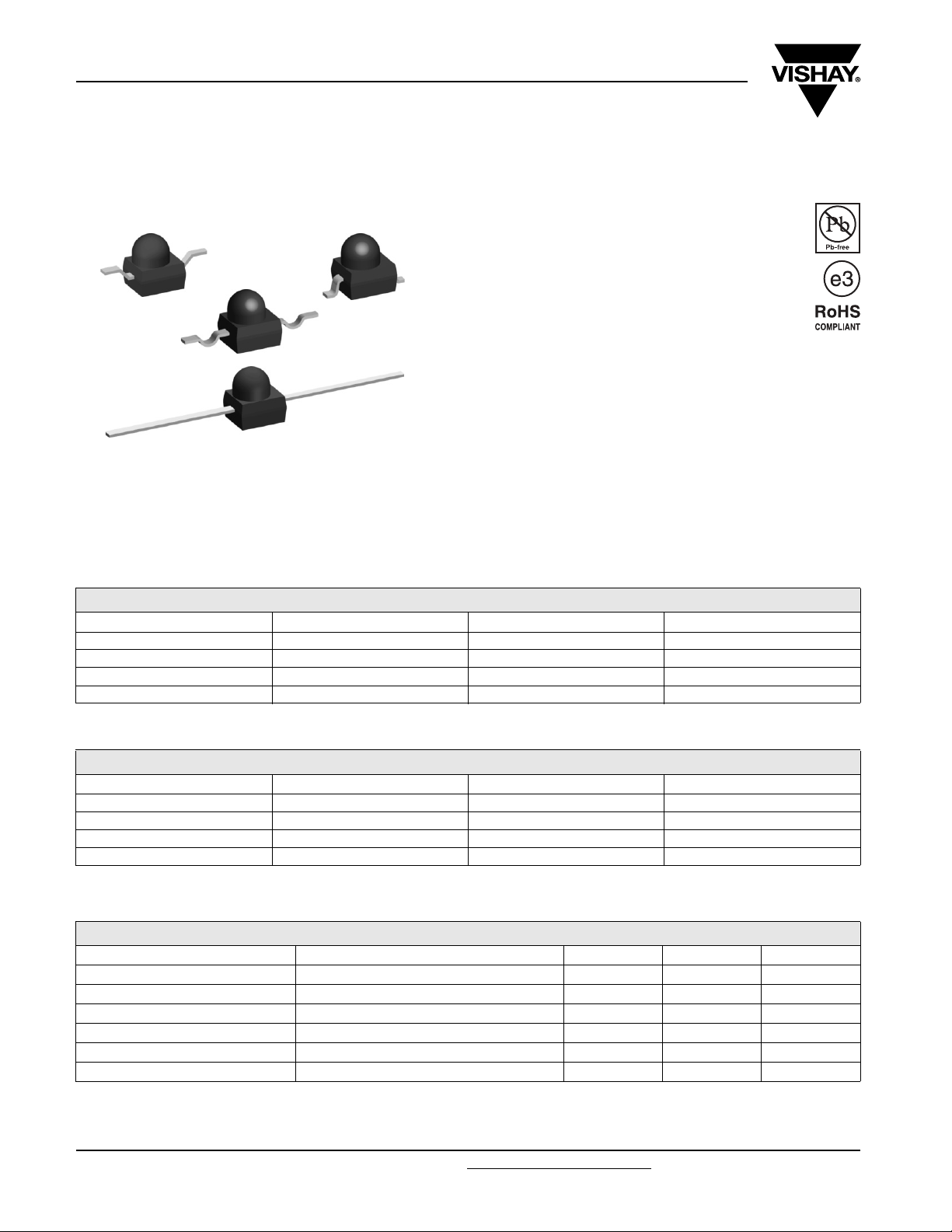
• Package type: surface mount
• Package form: GW, RGW, yoke, axial
TEMD1030
• Dimensions (L x W x H in mm): 2.5 x 2 x 2.7
2
• Radiant sensitive area (in mm
): 0.23
• High radiant sensitivity
• Daylight blocking filter matched with 870 nm to
950 nm emitters
TEMD1040
• Fast response times
• Angle of half sensitivity: ϕ = ± 15°
• Package matches with IR emitter series TSMF1000
18029
• Floor life: 168 h, MSL 3, acc. J-STD-020
• Lead (Pb)-free component in accordance with
DESCRIPTION
TEMD1000 series are PIN photodiodes with high speed and
high radiant sensitivity in black, surface mount plastic
packages with lens and daylight blocking filter. Filter
bandwidth is matched with 870 nm to 950 nm IR emitters.
RoHS 2002/95/EC and WEEE 2002/96/EC
APPLICATIONS
• High speed detector for infrared radiation
• Infrared remote control and free air data
transmissionsystems, e.g. in combination with TSFFxxxx
series IR emitters
PRODUCT SUMMARY
COMPONENT Ira (mA) ϕ (deg) λ
TEMD1000 12 ± 15 790 to 1050
TEMD1020 12 ± 15 790 to 1050
TEMD1030 12 ± 15 790 to 1050
TEMD1040 12 ± 15 790 to 1050
Note
Test conditions see table “Basic Characteristics”
0.5
(nm)
ORDERING INFORMATION
ORDERING CODE PACKAGING REMARKS PACKAGE FORM
TEMD1000 Tape and reel MOQ: 1000 pcs, 1000 pcs/reel Reverse gullwing
TEMD1020 Tape and reel MOQ: 1000 pcs, 1000 pcs/reel Gullwing
TEMD1030 Tape and reel MOQ: 1000 pcs, 1000 pcs/reel Yoke
TEMD1040 Bulk MOQ: 1000 pcs, 1000 pcs/bulk Axial leads
Note
MOQ: minimum order quantity
ABSOLUTE MAXIMUM RATINGS
PARAMETER TEST CONDITION SYMBOL VALUE UNIT
Reverse voltage V
Power dissipation T
Junction temperature T
Operating temperature range T
Storage temperature range T
Soldering temperature t ≤ 5 s T
Note
T
= 25 °C, unless otherwise specified
amb
www.vishay.com For technical questions, contact: detectortechsupport@vishay.com
436 Rev. 2.1, 08-Sep-08
≤ 25 °C P
amb
R
V
j
amb
stg
sd
60 V
75 mW
100 °C
- 40 to + 85 °C
- 40 to + 100 °C
< 260 °C
Document Number: 81564
Page 2
TEMD1000, TEMD1020, TEMD1030, TEMD1040
Silicon PIN Photodiode, RoHS Compliant
Vishay Semiconductors
BASIC CHARACTERISTICS
PARAMETER TEST CONDITION SYMBOL MIN. TYP. MAX. UNIT
Forward voltage I
Breakdown voltage I
Reverse dark current V
Diode capacitance V
E
e
Reverse light current
Temperature coefficient of I
ra
E
e
Absolute spectral sensitivity
Angle of half sensitivity
Wavelength of peak sensitivity λ
Range of spectral bandwidth λ
Rise time V
Fall time V
= 10 V, RL = 50 Ω, λ = 820 nm t
R
= 10 V, RL = 50 Ω, λ = 820 nm t
R
Note
T
= 25 °C, unless otherwise specified
amb
= 50 mA V
F
= 100 µA, E = 0 V
R
= 10 V, E = 0 I
R
= 5 V, f = 1 MHz, E = 0 C
R
= 1 mW/cm2, λ = 8 70 n m ,
V
= 5 V
R
= 1 mW/cm2, λ = 9 50 n m ,
V
= 5 V
R
VR = 5 V, λ = 870 nm, TK
V
= 5 V, λ = 870 nm s(λ)0.60A/W
R
V
= 5 V, λ = 950 nm s(λ)0.55A/W
R
(BR)
ro
I
ra
I
ra
F
60 V
D
512 µA
Ira
ϕ
p
0.5
r
f
11.3V
110nA
1.8 pF
10 µA
0.2 %/K
± 15 deg
940 nm
790 to 1050 nm
4ns
4ns
BASIC CHARACTERISTICS
T
= 25 °C, unless otherwise specified
amb
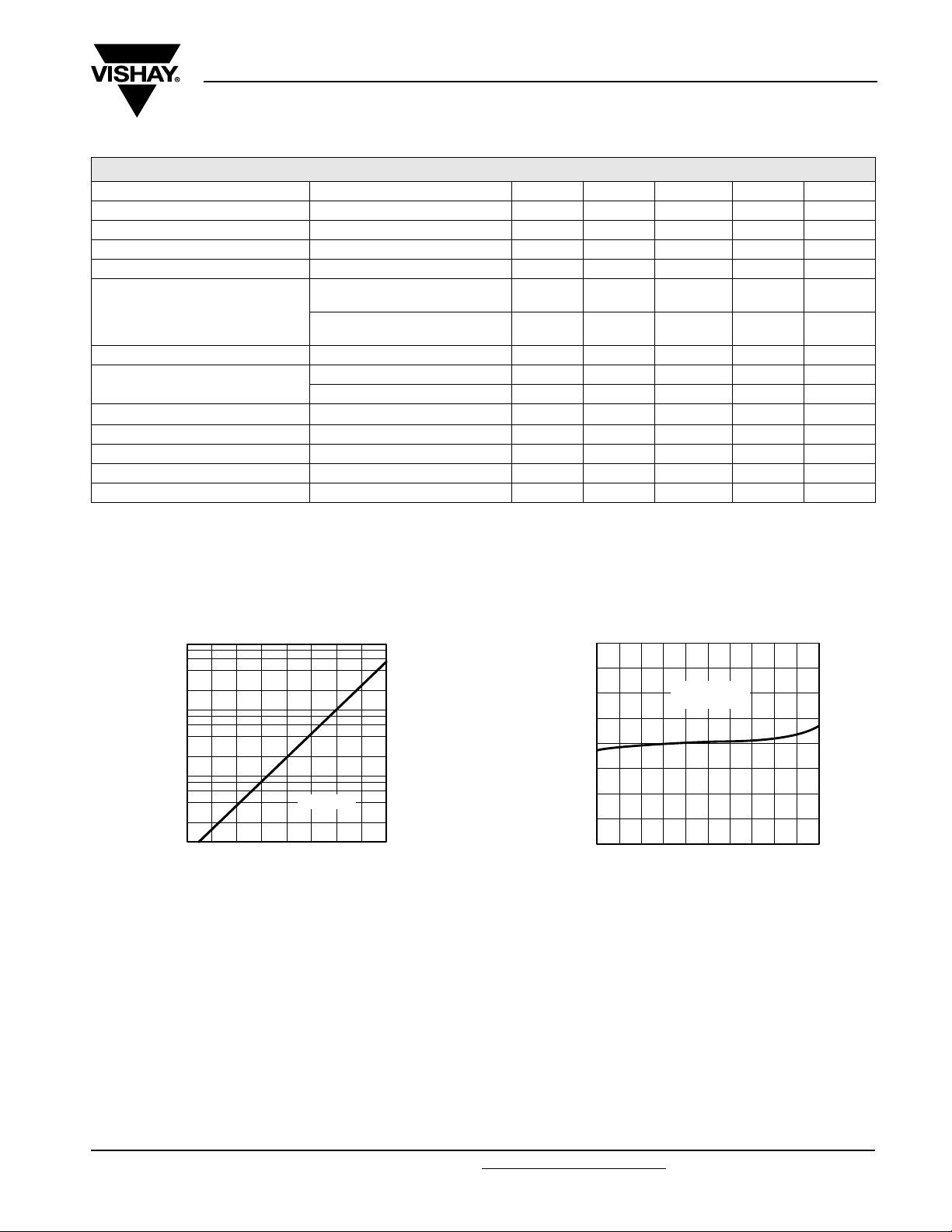
- Relative Reverse Light Current
ra, rel
I
94 8416
1.4
1.2
1.0
0.8
0.6
VR = 5 V
λ = 950 nm
4020
0
T
- Ambient Temperature (°C)
amb
60
1000
100
10
- Reverse Dark Current (nA)
ro
I
1
20
94 8427
T
- Ambient Temperature (°C)
amb
VR = 10 V
806040
100
Fig. 1 - Reverse Dark Current vs. Ambient Temperature Fig. 2 - Relative Reverse Light Current vs. Ambient Temperature
10080
Document Number: 81564 For technical questions, contact: detectortechsupport@vishay.com
www.vishay.com
Rev. 2.1, 08-Sep-08 437
Page 3
TEMD1000, TEMD1020, TEMD1030, TEMD1040
Vishay Semiconductors
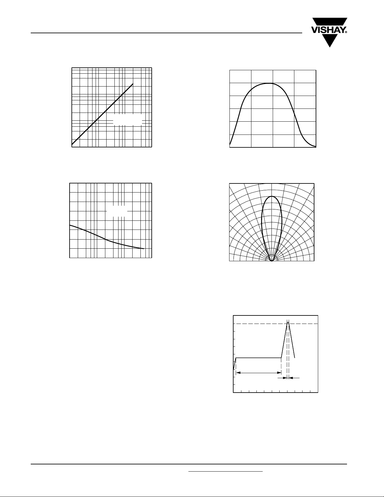
100
10
1.0
- Reverse Light Current (µA)
ra
I
0.1
0.01
16055
Fig. 3 - Reverse Light Current vs. Irradiance
8
6
4
0.1
Ee - Irradiance (mW/cm²)
E=0
f=1MHz
V
= 5 V
CE
λ
= 950 nm
1
Silicon PIN Photodiode, RoHS Compliant
1.2
1.0
0.8
0.6
0.4
- Relative Spectral Sensivity
rel
0.2
S(λ)
0.0
10
750 850 950 1050 1150
94 8426
λ - Wavelength (nm)
Fig. 5 - Relative Spectral Sensitivity vs. Wavelength
1.0
0.9
0°
10° 20°
30°
40°
50°
2
- Diode Capacitance (pF)
D
C
0
0.1
94 8430
1
VR- Reverse Voltage (V)
Fig. 4 - Diode Capacitance vs. Reverse Voltage
PRECAUTIONS FOR USE
0.8
- Relative Sensitivity
rel
S
0.7
10
100
94 8248
0.6
0.20.4
0
Fig. 6 - Relative Radiant Sensitivity vs. Angular Displacement
REFLOW SOLDER PROFILE
60°
70°
80°
ϕ - Angular Displacement
1. Over-current-proof
Customer must apply resistors for protection, otherwise
slight voltage shift will cause big current change (burn out will
happen).
2. Storage
2.1 Storage temperature and rel. humidity conditions are:
5 °C to 35 °C, R.H. 60 %.
2.2 Floor life must not exceed 168 h, acc. to JEDEC level 3,
J-STD-020.
Once the package is opened, the products should be
used within a week. Otherwise, they should be kept in a
damp proof box with desiccant.
Considering tape life, we suggest to use products within
one year from production date.
2.3 If opened more than one week in an atmosphere 5 °C to
260
240
220
200
180
160
140
120
Temperature (°C)
100
80
60
020406080 100 120 140 160 180 200 220
17172
+ 5 °C/s
60 s to 120 s
Time (s)
- 5 °C/s
5 s
Fig. 7 - Lead Tin (SnPb) Reflow Solder Profile
35 °C, R.H. 60 %, devices should be treated at 60 °C
± 5 °C for 15 h.
2.4 If humidity indicator in the package shows pink color
(normal blue), then devices should be treated with the
same conditions as 2.3.
www.vishay.com For technical questions, contact: detectortechsupport@vishay.com
438 Rev. 2.1, 08-Sep-08
Document Number: 81564
Page 4

TEMD1000, TEMD1020, TEMD1030, TEMD1040
Silicon PIN Photodiode, RoHS Compliant
PACKAGE DIMENSIONS in millimeters: TEMD1000
Vishay Semiconductors
16159
PACKAGE DIMENSIONS in millimeters: TEMD1020
3.8 ± 0.2
Ø 1.9 ± 0.2
0.85
0.3
0.15 ± 0.05
2.5 ± 0.2
1.1
2 ± 0.2
0.5
CA
0.4
0.75
1.4
± 0.2
2.7
4.5
± 0.1
2.3 ± 0.1
1 ± 0.1
16160
Document Number: 81564 For technical questions, contact: detectortechsupport@vishay.com
Rev. 2.1, 08-Sep-08 439
www.vishay.com
Page 5

TEMD1000, TEMD1020, TEMD1030, TEMD1040
Vishay Semiconductors
Silicon PIN Photodiode, RoHS Compliant
PACKAGE DIMENSIONS in millimeters: TEMD1030
16228
PACKAGE DIMENSIONS in millimeters: TEMD1040
16760
www.vishay.com For technical questions, contact: detectortechsupport@vishay.com
440 Rev. 2.1, 08-Sep-08
Document Number: 81564
Page 6

TEMD1000, TEMD1020, TEMD1030, TEMD1040
Silicon PIN Photodiode, RoHS Compliant
REEL DIMENSIONS in millimeters
±0.2
±0.5
60.2
±1
178
16
±1.5
13.2
Leader and trailer tape:
Parts mounted
Unreel direction
± 0.5
13
2
.
5
±0.5
Label posted here
Empty leader (400 mm, min.)
Vishay Semiconductors
X
Tape position
coming out from reel
X
Direction of pulling out
Empty trailer (200 mm, min.)
TAPING DIMENSIONS in millimeters: TEMD1000
3.05 ± 0.1
0.3
Top tape
Ø 1.55 ± 0.05
Anode
Push pin through hole
Feed direction
Quantity per reel: 1000 pcs or 5000 pcs
Drawing-No.: 9.800-5080.01-4
Issue: 3; 11.06.08
18033
4 ± 0.1
2 ± 0.05
1.75 ± 0.15.5 ± 0.05
12 ± 0.3
4 ± 0.1
18030
Document Number: 81564 For technical questions, contact: detectortechsupport@vishay.com
www.vishay.com
Rev. 2.1, 08-Sep-08 441
Page 7

TEMD1000, TEMD1020, TEMD1030, TEMD1040
Vishay Semiconductors
Silicon PIN Photodiode, RoHS Compliant
TAPING DIMENSIONS in millimeters: TEMD1020
3.05 ± 0.1
0.3
Top tape
Ø 1.55 ± 0.05
Anode
Push pin through hole
Feed direction
Quantity per reel: 1000 pcs or 5000 pcs
4 ± 0.1
2 ± 0.05
4 ± 0.1
1.75 ± 0.1
5.5 ± 0.05
12 ± 0.3
18031
TAPING DIMENSIONS in millimeters: TEMD1030
3.05 ± 0.1
0.3
Top tape
Ø 1.55 ± 0.05
Anode
Push pin through hole
Feed direction
Quantity per reel: 1000 pcs or 5000 pcs
4 ± 0.1
2 ± 0.05
1.75 ± 0.15.5 ± 0.05
12 ± 0.3
4 ± 0.1
18032
www.vishay.com For technical questions, contact: detectortechsupport@vishay.com
442 Rev. 2.1, 08-Sep-08
Document Number: 81564
Page 8

Legal Disclaimer Notice
Vishay
Disclaimer
All product specifications and data are subject to change without notice.
Vishay Intertechnology, Inc., its affiliates, agents, and employees, and all persons acting on its or their behalf
(collectively, “Vishay”), disclaim any and all liability for any errors, inaccuracies or incompleteness contained herein
or in any other disclosure relating to any product.
Vishay disclaims any and all liability arising out of the use or application of any product described herein or of any
information provided herein to the maximum extent permitted by law. The product specifications do not expand or
otherwise modify Vishay’s terms and conditions of purchase, including but not limited to the warranty expressed
therein, which apply to these products.
No license, express or implied, by estoppel or otherwise, to any intellectual property rights is granted by this
document or by any conduct of Vishay.
The products shown herein are not designed for use in medical, life-saving, or life-sustaining applications unless
otherwise expressly indicated. Customers using or selling Vishay products not expressly indicated for use in such
applications do so entirely at their own risk and agree to fully indemnify Vishay for any damages arising or resulting
from such use or sale. Please contact authorized Vishay personnel to obtain written terms and conditions regarding
products designed for such applications.
Product names and markings noted herein may be trademarks of their respective owners.
Document Number: 91000 www.vishay.com
Revision: 18-Jul-08 1
 Loading...