

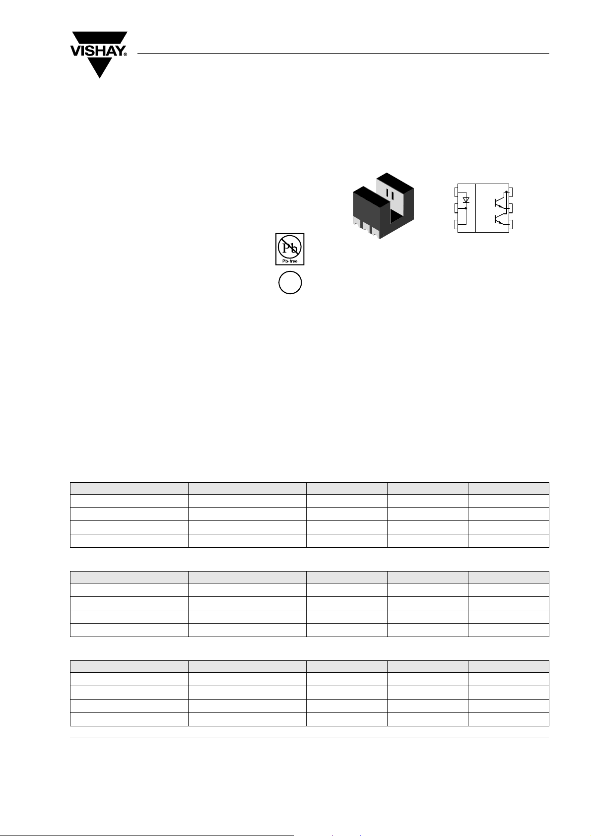
TCUT1200
Vishay Semiconductors
Subminiature Dual-Channel Transmissive Optical Sensor with
Phototransistor Outputs, RoHS Compliant, Released for
Lead (Pb)-free Solder Process
Description
The TCUT1200 is a compact transmissive sensor that
includes an infrared emitter and two phototransistor
detectors, located face-to-face in a surface-mount
package.
Features
• Package type: Surface-mount
• Detector type: Phototransistor
• Dimensions:
L 5 mm x W 4 mm x H 4 mm
• Gap: 2 mm
• Aperture: 0.3 mm
• Channel distance (center to center): 0.8 mm
• Typical output current under test: I
= 0.5 mA
C
• Emitter wavelength: 950 nm
• Lead (Pb)-free soldering released
• Lead (Pb)-free component in accordance with
RoHS 2002/95/EC and WEEE 2002/96/EC
• Minimum order quantity: 2000 pcs, 2000 pcs/reel
e4
Applications
• Accurate position sensor for encoder
• Detection of motion direction
• Computer mouse and trackballs
A Coll
Cath
Cath
E
E
19151
Absolute Maximum Ratings
T
= 25 °C, unless otherwise specified
amb
Coupler
Parameter Test condition Symbol Val ue Unit
≤ 25 °C
Power dissipation
Ambient temperature range
Storage temperature range
Soldering temperature in accordance with fig. 13
Input (Emitter)
Parameter Test condition Symbol Val ue Unit
Reverse voltage
Forward current
Forward surge current
Power dissipation
Output (Detector)
Parameter Test condition Symbol Val ue Unit
Collector emitter voltage
Emitter collector voltage
Collector current
Power dissipation
T
amb
≤ 10 µs I
t
p
≤ 25 °C P
T
amb
T
≤ 25 °C P
amb
P150mW
T
V
V
amb
T
T
V
I
FSM
CEO
ECO
I
stg
sd
R
F
V
C
V
- 40 to + 85 °C
- 40 to + 100 °C
260 °C
5V
25 mA
100 mA
75 mW
70 V
7V
20 mA
75 mW
Document Number 83755
Rev. 2.2, 13-Mar-07
www.vishay.com
1
TCUT1200
Vishay Semiconductors
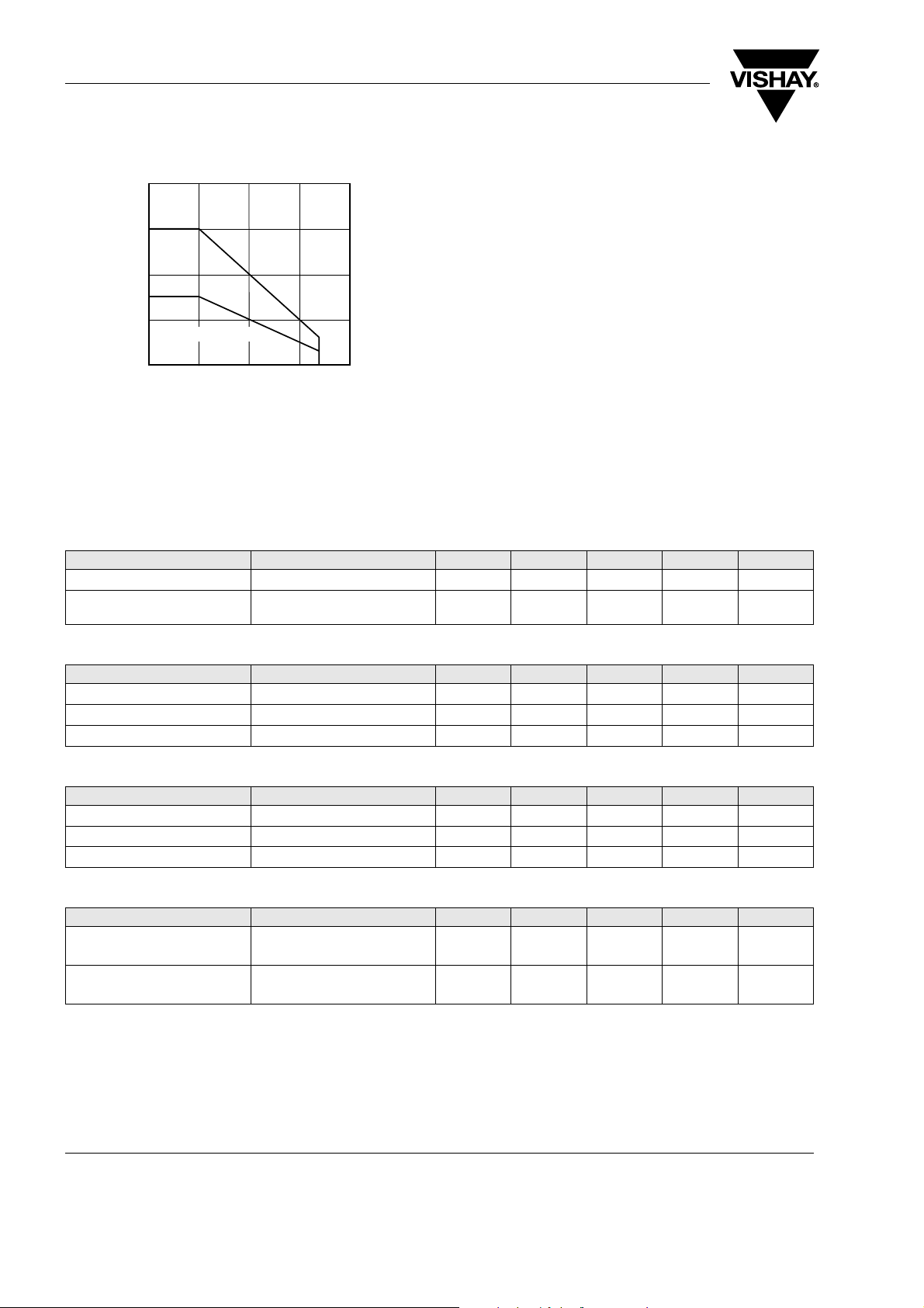
200
Sensor
Emitter/Detector
5025
T
- Ambient Temperature (°C)
amb
100
75
P - Power Dissipation (mW)
16538
150
100
50
0
0
Figure 1. Power Dissipation Limit vs. Ambient Temperature
Electrical Characteristics
T
= 25 °C, unless otherwise specified
amb
Coupler
Paramete r Test condition Symbol Min Ty p. Max Unit
= 5 V, IF = 15 mA I
Collector current per channel
Collector emitter saturation
voltage
Input (Emitter)
Paramete r Test condition Symbol Min Ty p. Max Unit
Forward voltage
Reverse current
Junction capacitance
V
CE
I
= 15 mA, IC = 0.05 mA V
F
= 15 mA V
I
F
= 5 V I
V
R
= 0 V, f = 1 MHz C
V
R
C
CEsat
F
R
j
300 500 µA
0.4 V
1.2 1.5 V
10 µA
50 pF
Output (Detector)
Paramete r Test condition Symbol Min Ty p. Max Unit
Collector emitter voltage
Emitter collector voltage
Collector dark current
Switching Characteristics
Paramete r Test condition Symbol Min Ty p. Max Unit
Rise time I
Fall time I
www.vishay.com
2
= 1 mA V
I
C
= 100 µA V
I
E
= 25 V, IF = 0, E = 0 I
V
CE
= 0.3 mA, VCE = 5 V,
C
= 1000 Ω (see figure 3)
R
L
= 0.3 mA, VCE = 5 V,
C
= 1000 Ω (see figure 3)
R
L
CEO
ECO
CEO
t
t
70 V
7V
10 100 nA
r
f
20.0 150 µs
30.0 150 µs
Document Number 83755
Rev. 2.2, 13-Mar-07
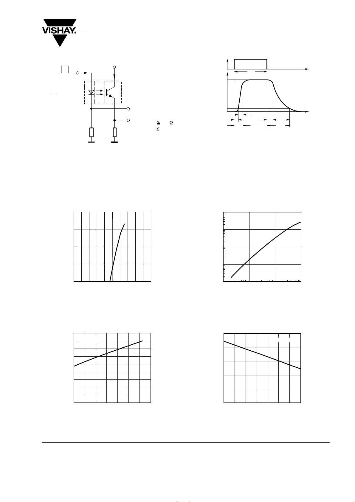
I
C
(
)
366
C
S
I
F
0
F
+ 5 V
I
C
R G = 50 Ω
t
p
= 20
T
t p = 1 ms
Channel I
Channel II
50 Ω 1000 Ω
16536
Figure 2. Test Circuit for tr and t
Typical Characteristics
T
= 25 °C, unless otherwise specified
amb
adjusted by I
Oscilloscope
RL 1 M
C
f
L
F
20 pF
t
p
t
d
t
r
t
(= t + t )
on
96 11698
I
F
0
I
C
100 %
90 %
10 %
0
t
r
t
d
t
on
pulse duration
delay time
rise time
turn-on time
r
d
Figure 3. Switching Times
TCUT1200
Vishay Semiconductors
t
p
t
f
t
s
t
off
t
s
t
f
t
(= ts+tf)turn-off time
off
t
t
storage time
fall time
1000
10
V CE= 5 V
100
mA
10
urrent
1
F
I - Forward
13660
0.1
0
0.2
0.60.4
0.8 2.0
1.0
V
- Forward Voltage (V)
F
1.2
1.4
1.6
1.8
Figure 4. Forward Current vs. Forward Voltage
0.18
I F = 15 mA
0.16
0.14
0.12
0.10
aturation Voltage (V)
0.08
I
C
= 50 µA
1
0.1
0.01
C
I - Collector Current (mA)
0.001
13665
0.1
1
I
- Forward Current (mA)
F
10
100
Figure 6. Collector Current vs. Forward Current
1.3
I F = 15 mA
1.2
1.1
1.0
0.06
0.04
oll. Emitter
0.02
0
CEsat
- 40
V -
1
2
- Ambient Temperature (°C)
T
amb
40
200- 20
60
100
80
Figure 5. Collector Emitter Saturation Voltage vs.
F
0.9
V - Forward Voltage (V)
13661
0.8
- 40
- 20
T
amb
20
0
40
- Ambient Temperature (°C)
60
100
80
Figure 7. Forward Voltage vs. Ambient Temperature
Ambient Temperature
Document Number 83755
Rev. 2.2, 13-Mar-07
www.vishay.com
3

TCUT1200
C
C
C
C
s
/
/
Vishay Semiconductors
1.0
V CE= 5 V
0.9
0.8
0.7
0.6
urrent (mA)
0.5
IF= 15 mA
0.4
0.3
ollector
C
I -
13663
0.2
0.1
0
- 40
20 0- 20
T
- Ambient Temperature (°C)
amb
40
I F= 5 mA
80
60
100
Figure 8. Collector Current vs. Ambient Temperature
10000
V CE= 10 V
I
= 0
1000
F
urrent (nA)
100
ollector Dark
10
CEO
I -
1
96 11875
40
20
0
30
10
T
- Ambient Temperature (°C)
amb
60
50
70
100 90
80
Figure 9. Collector Dark Current vs. Ambient Temperature
100
90
80
70
60
50
Fall Time (µs)
40
30
- Rise
f
t
r
t
16552
20
10
0
0
250
t
f
t
r
1000
750
500
I
- Collector Current (µA)
C
1250
1750 1500
Figure 11. Rise/Fall Time vs. Collector Current
I
= 15 mA + V C = 5 V
F
74HCT14
U
13887
GND
10 kΩ
V
E
Figure 12. Application example
2000
Q
1.25
1
s
0.75
0.5
0.25
Crel
I - Relative Collector Current
0
- 1.5
13657
- 0.5
- 1
s - Displacement (mm)
0.5
0
1.51
Figure 10. Relative Collector Current vs. Displacement
www.vishay.com
4
Document Number 83755
Rev. 2.2, 13-Mar-07

Reflow Solder Profiles Drypack
Devices are packed in moisture barrier bags (MBB) to
prevent the products from absorbing moisture during
280
260
240
220
200
180
160
140
Temperature (°C)
120
100
80
4 °C/s MAX
Pre-heating time:
90 ± 30 s
4 °C/s MAX
180 °C
150 °C
260 °C
230 °C
Heating time:
30 ± 10 s
Time (s)
Figure 13. Lead (Pb)-free (Sn) Reflow Solder Profile
19152
transportation and storage. Each bag contains a desiccant.
Floor Life
Floor life (time between soldering and removing from
MBB) must not exceed the time indicated in
J-STD-020. According JEDEC, J-STD-020, this component is released to Moisture Sensitivity Level 2, for
use of Lead Tin (SnPb) Reflow Solder Profile
(Figure 14) or Level 3, for use of Lead (Pb)-free (Sn)
Reflow Solder Profile (Figure 13).
Floor Life: 12 month (Level 2) or 168 hours (Level 3)
Floor Conditions: T
Drying
In case of moisture absorption, devices should be
280
260
240
220
200
180
160
140
Temperature (°C)
120
100
80
4 °C/s MAX
240 °C
4 °C/s MAX
180 °C
150 °C
Pre-heating time:
90 ± 30 s
Time (s)
230 °C
Heating time:
10 - 20 s
Figure 14. Lead Tin (SnPb) Reflow Solder Profile
19153
baked before soldering. Conditions see J-STD-020 or
Label. Devices taped on reel dry using recommended
conditions 192 h at 40 °C (± 5 °C), RH < 5 % or 96 h
at 60 °C (± 5 °C), RH < 5 %.
TCUT1200
Vishay Semiconductors
< 30 °C, RH < 60 %
amb
Document Number 83755
Rev. 2.2, 13-Mar-07
www.vishay.com
5

TCUT1200
Vishay Semiconductors
Dimensions of Reel and Tape in millimeters
Dimensions of Tape in millimeters
13722
www.vishay.com
6
13720
Document Number 83755
Rev. 2.2, 13-Mar-07

Package Dimensions
TCUT1200
Vishay Semiconductors
Document Number 83755
Rev. 2.2, 13-Mar-07
19311
www.vishay.com
7

TCUT1200
Vishay Semiconductors
Ozone Depleting Substances Policy Statement
It is the policy of Vishay Semiconductor GmbH to
1. Meet all present and future national and international statutory requirements.
2. Regularly and continuously improve the performance of our products, processes, distribution and operating
systems with respect to their impact on the health and safety of our employees and the public, as well as
their impact on the environment.
It is particular concern to control or eliminate releases of those substances into the atmosphere which are
known as ozone depleting substances (ODSs).
The Montreal Protocol (1987) and its London Amendments (1990) intend to severely restrict the use of ODSs
and forbid their use within the next ten years. Various national and international initiatives are pressing for an
earlier ban on these substances.
Vishay Semiconductor GmbH has been able to use its policy of continuous improvements to eliminate the use
of ODSs listed in the following documents.
1. Annex A, B and list of transitional substances of the Montreal Protocol and the London Amendments
respectively
2. Class I and II ozone depleting substances in the Clean Air Act Amendments of 1990 by the Environmental
Protection Agency (EPA) in the USA
3. Council Decision 88/540/EEC and 91/690/EEC Annex A, B and C (transitional substances) respectively.
Vishay Semiconductor GmbH can certify that our semiconductors are not manufactured with ozone depleting
substances and do not contain such substances.
We reserve the right to make changes to improve technical design
and may do so without further notice.
Parameters can vary in different applications. All operating parameters must be validated for each customer
application by the customer. Should the buyer use Vishay Semiconductors products for any unintended or
unauthorized application, the buyer shall indemnify Vishay Semiconductors against all claims, costs, damages,
and expenses, arising out of, directly or indirectly, any claim of personal damage, injury or death associated
with such unintended or unauthorized use.
Vishay Semiconductor GmbH, P.O.B. 3535, D-74025 Heilbronn, Germany
www.vishay.com
8
Document Number 83755
Rev. 2.2, 13-Mar-07

Legal Disclaimer Notice
Vishay
Notice
Specifications of the products displayed herein are subject to change without notice. Vishay Intertechnology, Inc.,
or anyone on its behalf, assumes no responsibility or liability for any errors or inaccuracies.
Information contained herein is intended to provide a product description only. No license, express or implied, by
estoppel or otherwise, to any intellectual property rights is granted by this document. Except as provided in Vishay's
terms and conditions of sale for such products, Vishay assumes no liability whatsoever, and disclaims any express
or implied warranty, relating to sale and/or use of Vishay products including liability or warranties relating to fitness
for a particular purpose, merchantability, or infringement of any patent, copyright, or other intellectual property right.
The products shown herein are not designed for use in medical, life-saving, or life-sustaining applications.
Customers using or selling these products for use in such applications do so at their own risk and agree to fully
indemnify Vishay for any damages resulting from such improper use or sale.
Document Number: 91000 www.vishay.com
Revision: 08-Apr-05 1
 Loading...