


Transmissive Optical Sensor
Description
This device has a compact construction where the
emitting-light sources and the detectors are located
face to face on the same optical axes.
The operating wavelength is 950 nm. The detector
consists of a photologic-IC with Schmitt trigger and
open collector output.
Applications
D
Detection of opaque material, documents etc.
D
Paper position sensor in copy machines
D
Position sensor for shaft encoder
TCSS1100/ TCSS2100
Vishay Semiconductors
B)
A)
15132
Features
+
95 10821
V
O
D
Output:
‘LOW’ when infrared beam is not interrupted
D
Inverter-open collector
D
TTL compatible
D
Built-in voltage regulator
D
Plastic polycarbonate case, protected against
ambient light
D
No adjustment necessary
D
Two package variations
+
_
7.6
0.3”
Top view
Handling Precautions
Connect a capacitor C of more than 100 nF between VS1 and ground in order to stabilize power supply voltage!
Order Instruction
Ordering Code Resolution (mm) / Aperture (mm) Remarks
TCSS1100
TCSS2100
A)
B)
0.6 / 1.0 No mounting flags
0.6 / 1.0 With two mounting flags
Rev. A4, 08–Jun–99
www.vishay.comDocument Number 83761
1 (7)

TCSS1100/ TCSS2100
yg
ygg
Vishay Semiconductors
Absolute Maximum Ratings
Input (Emitter)
Parameter Test Conditions Symbol Value Unit
Reverse voltage V
Forward current I
Forward surge current tp ≤ 10ms I
Power dissipation T
Junction temperature T
Output (Detector)
Parameter Test Conditions Symbol Value Unit
Supply voltages V
Output current I
Power dissipation T
Junction temperature T
≤ 25°C P
amb
≤ 25°C P
amb
F
FSM
S1
V
S2
O
R
6 V
60 mA
3 A
V
j
100 mW
100
°
C
6.5 V
18 V
20 mA
V
j
250 mW
100
°
C
Coupler
Parameter Test Conditions Symbol V alue Unit
Total power dissipation T
Ambient temperature range T
Storage temperature range T
Soldering temperature 2 mm from case, t ≤ 5 s T
Electrical Characteristics (T
≤ 25°C P
amb
= 25°C)
amb
tot
amb
stg
sd
250 mW
–25 to +85
–40 to +100
260
Input (Emitter)
Parameter Test Conditions Symbol Min. Typ. Max. Unit
Forward voltage IF = 50 mA V
Junction capacitance VR = 0, f = 1 MHz C
F
j
1.25 1.6 V
50 pF
Output (Detector)
Parameter Test Conditions Symbol Min. Typ. Max. Unit
Supply voltage range V
S1
V
S2
4.75 5.25 V
4.0 16 V
Coupler
Parameter Test Conditions Symbol Min. Typ. Max. Unit
Supply current VS1 = 16 V I
Output current VS1 = VS2 = 16 V, IF = 0 I
Input threshold current VS1 = 5 V I
Hysteresis VS1 = 5 V I
Foff/IFon
Output voltage IOL = 16 mA, IF ≥ ITF, VS1 = 5 V V
Switching frequency IF 3x IFT, VS1 = VS2 = 5 V,
RL = 1 k
W
OH
f
S1
FT
OL
sw
3 5 mA
5 10 mA
80 %
0.15 0.4 V
200 kHz
°
C
°
C
°
C
1
m
A
www.vishay.com
2 (7) Rev. A4, 08–Jun–99
Document Number 83761

TCSS1100/ TCSS2100
S1 S2 F FT L
(g)
Vishay Semiconductors
Switching Characteristics
Parameter Test Conditions Symbol Typ. Unit
Rise time VS1 = VS2 = 5 V, IF = 3 x IFT, RL = 1 kW (see figure 1) t
Turn-on time
Fall time t
Turn-off time t
r
t
on
f
off
50.0 ns
1.0
20.0 ns
3.0
m
s
m
s
Rev. A4, 08–Jun–99
www.vishay.comDocument Number 83761
3 (7)
TCSS1100/ TCSS2100
Vishay Semiconductors
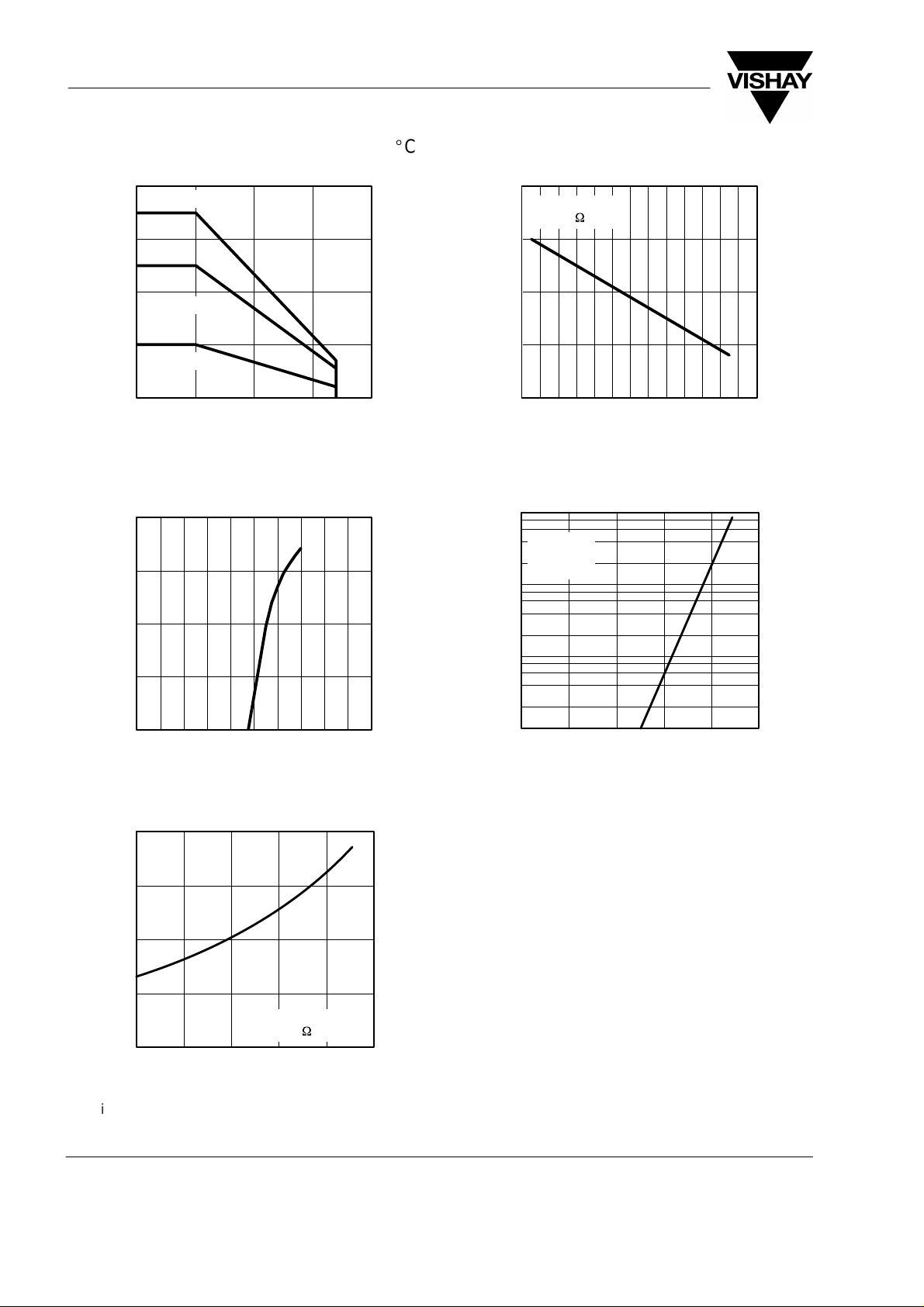
Typical Characteristics (T
400
Coupled device
300
200
Photodetector
100
tot
P – Total Power Dissipation ( mW )
96 11945
1000.0
IR-diode
0
0 255075100
T
– Ambient Temperature ( °C )
amb
Figure 4. Total Power Dissipation vs.
Ambient Temperature
100.0
= 25_C, unless otherwise specified)
amb
1.2
VS1=VS2=5V
R
=1k
W
L
1.1
1.0
0.9
Srel
I – Relative Supply Current
0.8
–30–20–10 0 10 20 30 40 50 60 70 80 90100
T
– Ambient Temperature ( °C )96 11946
amb
Figure 7. Relative Supply Current vs.
Ambient Temperature
1000
VS1=5V
V
=20V
S2
I
=0
F
100
10.0
1.0
F
I – Forward Current ( mA )
0.1
0 0.2 0.4 0.6 0.8 1.0 1.2 1.4 1.6 1.8 2.0
VF – Forward Voltage ( V )96 11862
Figure 5. Forward Current vs. Forward Voltage
2.0
1.5
1.0
0.5
VS1=VS2=5V
R
=1k
FTrel
I – Relative Threshold Forward Current
95 11080
0
–25 0 25 50
T
– Ambient Temperature ( °C )
amb
W
L
75
100
10
OH
I – High Level Output Current ( nA )
1
–250 255075
T
95 11079
– Ambient Temperature ( °C )
amb
Figure 8. High Level Output Current vs.
Ambient Temperature
100
Figure 6. Relative Threshold Forward Current vs.
Ambient Temperature
www.vishay.com
4 (7) Rev. A4, 08–Jun–99
Document Number 83761

Dimensions of TCSS1100 in mm
TCSS1100/ TCSS2100
Vishay Semiconductors
Rev. A4, 08–Jun–99
96 12096
www.vishay.comDocument Number 83761
5 (7)

TCSS1100/ TCSS2100
Vishay Semiconductors
Dimensions of TCSS2100 in mm
96 12097
www.vishay.com
6 (7) Rev. A4, 08–Jun–99
Document Number 83761

TCSS1100/ TCSS2100
Vishay Semiconductors
Ozone Depleting Substances Policy Statement
It is the policy of Vishay Semiconductor GmbH to
1. Meet all present and future national and international statutory requirements.
2. Regularly and continuously improve the performance of our products, processes, distribution and operating
systems with respect to their impact on the health and safety of our employees and the public, as well as
their impact on the environment.
It is particular concern to control or eliminate releases of those substances into the atmosphere which are known as
ozone depleting substances (ODSs).
The Montreal Protocol (1987) and its London Amendments (1990) intend to severely restrict the use of ODSs and
forbid their use within the next ten years. V arious national and international initiatives are pressing for an earlier ban
on these substances.
Vishay Semiconductor GmbH has been able to use its policy of continuous improvements to eliminate the use of
ODSs listed in the following documents.
1. Annex A, B and list of transitional substances of the Montreal Protocol and the London Amendments respectively
2. Class I and II ozone depleting substances in the Clean Air Act Amendments of 1990 by the Environmental
Protection Agency (EPA) in the USA
3. Council Decision 88/540/EEC and 91/690/EEC Annex A, B and C (transitional substances) respectively.
Vishay Semiconductor GmbH can certify that our semiconductors are not manufactured with ozone depleting
substances and do not contain such substances.
We reserve the right to make changes to improve technical design and may do so without further notice.
Parameters can vary in different applications. All operating parameters must be validated for each customer application
by the customer. Should the buyer use Vishay Semiconductors products for any unintended or unauthorized application, the
buyer shall indemnify Vishay Semiconductors against all claims, costs, damages, and expenses, arising out of, directly or
indirectly , any claim of personal damage, injury or death associated with such unintended or unauthorized use.
Rev. A4, 08–Jun–99
Vishay Semiconductor GmbH, P.O.B. 3535, D-74025 Heilbronn, Germany
Telephone: 49 (0)7131 67 2831, Fax number: 49 (0)7131 67 2423
www.vishay.comDocument Number 83761
7 (7)

Legal Disclaimer Notice
Vishay
Document Number: 91000 www.vishay.com
Revision: 08-Apr-05 1
Notice
Specifications of the products displayed herein are subject to change without notice. Vishay Intertechnology, Inc.,
or anyone on its behalf, assumes no responsibility or liability for any errors or inaccuracies.
Information contained herein is intended to provide a product description only. No license, express or implied, by
estoppel or otherwise, to any intellectual property rights is granted by this document. Except as provided in Vishay's
terms and conditions of sale for such products, Vishay assumes no liability whatsoever, and disclaims any express
or implied warranty, relating to sale and/or use of Vishay products including liability or warranties relating to fitness
for a particular purpose, merchantability, or infringement of any patent, copyright, or other intellectual property right.
The products shown herein are not designed for use in medical, life-saving, or life-sustaining applications.
Customers using or selling these products for use in such applications do so at their own risk and agree to fully
indemnify Vishay for any damages resulting from such improper use or sale.
 Loading...