

查询TCLT11供应商
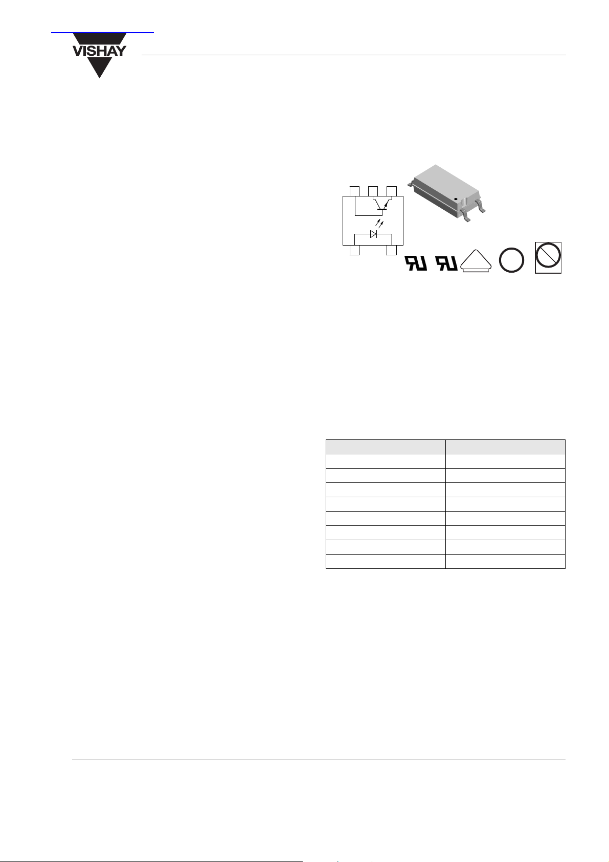
TCLT11.. Series
Vishay Semiconductors
Optocoupler, Phototransistor Output, SOP-6L5, Half Pitch, Long
Mini-Flat Package
Features
• SMD Low profile 5 pin package
• Isolation Test Voltage 5000 V
• CTR flexibility available see order information
• Special construction
• Extra low coupling capacitance
• Connected base
• DC input with transistor output
• Lead-free component
• Component in accordance to RoHS 2002/95/EC
and WEEE 2002/96/EC
RMS
543
12
C
17296
V
D E
e3
Pb
Pb-free
Agency Approvals
• UL1577, File No. E76222 System Code W, Double
Protection
• CSA 93751
• BSI IEC60950 IEC60065
• DIN EN 60747-5-2 (VDE0884)
DIN EN 60747-5-5 pending
• FIMKO
•NOTE:
See the Safety Standard Approval List "Agency
Table" for more detailed information.
Applications
Switchmode power supplies
Computer peripheral interface
Microprocessor system interface
Description
The TCLT11.. Series consists of a phototransistor
optically coupled to a gallium arsenide infrared-emitting diode in a 5-lead SOP5L package.
The elements are mounted on one leadframe providing a fixed distance between input and output for highest safety requirements.
Order Information
Part Remarks
TCLT1100 CTR 50 - 600 %, SMD-5
TCLT1102 CTR 63 - 125 %, SMD-5
TCLT1103 CTR 100 - 200 %, SMD-5
TCLT1105 CTR 50 - 150 %, SMD-5
TCLT1106 CTR 100 - 300 %, SMD-5
TCLT1107 CTR 80 - 160 %, SMD-5
TCLT1108 CTR 130 - 260 %, SMD-5
TCLT1109 CTR 200 - 400 %, SMD-5
NOTE: Available only on tape and reel.
Document Number 83514
Rev. 1.8, 03-Dec-04
www.vishay.com
1
TCLT11.. Series
Vishay Semiconductors
Absolute Maximum Ratings
T
= 25 °C, unless otherwise specified
amb
Stresses in excess of the absolute Maximum Ratings can cause permanent damage to the device. Functional operation of the device is
not implied at these or any other conditions in excess of those given in the operational sections of this document. Exposure to absolute
Maximum Rating for extended periods of the time can adversely affect reliability.
Input
Parame te r Test condition Symbol Val ue Unit
Reverse voltage V
Forward current I
Forward surge current t
≤ 10 µsI
p
Power dissipation P
Junction temperature T
Output
Parame te r Test condition Symbol Val ue Unit
Collector emitter voltage V
Emitter collector voltage V
Collector current I
Collector peak current t
Power dissipation P
Junction temperature T
/T = 0.5, tp ≤ 10 ms I
p
R
F
FSM
diss
j
CEO
ECO
C
CM
diss
j
6V
60 mA
1.5 A
100 mW
125 °C
70 V
7V
50 mA
100 mA
150 mW
125 °C
Coupler
Parame te r Test condition Symbol Val ue Unit
Isolation test voltage (RMS) V
Total power dissipation P
Operating ambient temperature
T
ISO
tot
amb
5000 V
RMS
250 mW
- 40 to + 100 °C
range
Storage temperature range T
Soldering temperature T
stg
sld
- 40 to + 100 °C
240 °C
Electrical Characteristics
T
= 25 °C, unless otherwise specified
amb
Minimum and maximum values are testing requirements. Typical values are characteristics of the device and are the result of engineering
evaluation. Typical values are for information only and are not part of the testing requirements.
Input
Parame te r Test condition Symbol Min Ty p. Max Unit
Forward voltage I
Junction capacitance V
= ± 50 mA V
F
= 0 V, f = 1 MHz C
R
F
j
1.25 1.6 V
50 pF
Output
Parame te r Test condition Symbol Min Ty p. Max Unit
Collector emitter voltage I
Emitter collector voltage I
Collector-emitter cut-off current V
= 1 mA V
C
= 100 µAV
E
= 20 V, If = 0, E = 0 I
CE
CEO
ECO
CEO
70 V
7V
10 100 nA
www.vishay.com
2
Document Number 83514
Rev. 1.8, 03-Dec-04
Coupler
Parameter Test condition Symbol Min Ty p . Max Unit
Collector emitter saturation
voltage
Cut-off frequency V
Coupling capacitance f = 1 MHz C
= 10 mA, IC = 1 mA V
I
F
= 5 V, IF = 10 mA,
CE
= 100 Ω
R
L
Current Transfer Ratio
Parameter Test condition Part Symbol Min Ty p. Max Unit
I
C/IF
VCE = 5 V, IF = 5 mA TCLT1100 CTR 50 600 %
V
= 5 V, IF = 10 mA TCLT1102 CTR 63 125 %
CE
TCLT1103 CTR 100 200 %
= 5 V, IF = 1 mA TCLT1102 CTR 22 45 %
V
CE
TCLT1103 CTR 34 70 %
TCLT1104 CTR 56 100 %
= 5 V, IF = 5 mA TCLT1105 CTR 50 150 %
V
CE
TCLT1106 CTR 100 300 %
TCLT1107 CTR 80 160 %
TCLT1108 CTR 130 260 %
TCLT1109 CTR 200 400 %
CEsat
f
c
k
TCLT11.. Series
Vishay Semiconductors
0.3 V
110 kHz
0.3 pF
Maximum Safety Ratings
(according to DIN EN 60747-5-2(VDE0884)/ DIN EN 60747-5-5 pending) see figure 1
This optocoupler is suitable for safe electrical isolation only within the safety ratings.
Compliance with the safety ratings shall be ensured by means of suitable protective circuits.
Input
Parameter Test condition Symbol Min Ty p . Max Unit
Forward current I
F
Output
Parameter Test condition Symbol Min Ty p . Max Unit
Power dissipation P
diss
Coupler
Parameter Test condition Symbol Min Ty p . Max Unit
Rated impulse voltage V
Safety temperature T
IOTM
si
130 mA
265 mW
8kV
150 °C
Document Number 83514
Rev. 1.8, 03-Dec-04
www.vishay.com
3
TCLT11.. Series
Vishay Semiconductors
Insulation Rated Parameters
Parame te r Test condition Symbol Min Ty p. Max Unit
Partial discharge test voltage Routine test
Partial discharge test voltage Lot test (sample test)
Insulation resistance V
4.8
4.4
1.40
1.27
100 %, t
test
= 60 s, t
t
Tr
(see figure 2)
= 500 V R
IO
V
= 500 V, T
IO
V
= 500 V, T
IO
(construction test only)
= 1 s V
= 10 s,
test
= 100 °C R
amb
= 150 °C
amb
V
pd
IOTM
V
pd
IO
IO
R
IO
V
IOTM
V
IOWM
V
IORM
1.6 kV
8kV
1.3 kV
12
10
11
10
9
10
t1, t2 = 1 to 10 s
t
, t4 = 1 s
3
t
= 10 s
test
= 12 s
t
stres
V
Pd
Ω
Ω
Ω
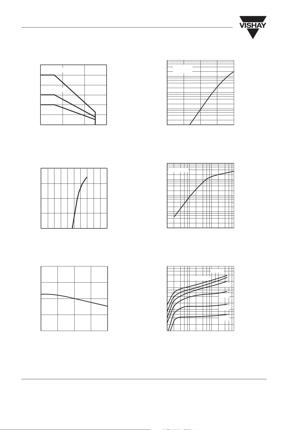
Figure 1. Derating diagram
13930
0
t
1
tTr = 60 s
t
2
t
t3t
test
t
stres
4
t
Figure 2. Test pulse diagram for sample test according to DIN EN
60747-5-2(VDE0884)/ DIN EN 60747-; IEC60747
www.vishay.com
4
Document Number 83514
Rev. 1.8, 03-Dec-04

Switching Characteristics
Parameter Test condition Symbol Min Ty p . Max Unit
Delay time V
Rise time V
Turn-on time V
Storage time V
Fall time V
Turn-off time V
Turn-on time V
Turn-off time V
= 5 V, IC = 2 mA, RL = 100 Ω
S
(see figure 3)
= 5 V, IC = 2 mA, RL = 100 Ω
S
(see figure 3)
= 5 V, IC = 2 mA, RL = 100 Ω
S
(see figure 3)
= 5 V, IC = 2 mA, RL = 100 Ω
S
(see figure 3)
= 5 V, IC = 2 mA, RL = 100 Ω
S
(see figure 3)
= 5 V, IC = 2 mA, RL = 100 Ω
S
(see figure 3)
= 5 V, IF = 10 mA, RL = 1 kΩ
S
(see figure 4)
= 5 V, IF = 10 mA, RL = 1 kΩ
S
(see figure 4)
TCLT11.. Series
Vishay Semiconductors
t
d
t
r
t
on
t
s
t
f
t
off
t
on
t
off
3.0 µs
3.0 µs
6.0 µs
0.3 µs
4.7 µs
5.0 µs
9.0 µs
10.0 µs
+ 5 V
IC = 2 mA;
Channel I
Channel II
95 10804
I
0
RG = 50 W
t
p
= 0.01
T
tp = 50 Ps
I
F
F
50 W 100 W
Figure 3. Test circuit, non-saturated operation
1k
Ω
+5V
I
C
Channel I
Channel II
0
RG=50
t
p
= 0.01
T
tp=50 s
I
F
Ω
µ
IF=10mA
Ω
50
adjusted through
input amplitude
Oscilloscope
R
= 1 MW
L
= 20 pF
C
L
Oscilloscope
Ω
M1
R
≥
L
20 pF
C
≤
L
I
F
0
I
C
100%
90%
10%
0
t
d
t
t
p
t
d
t
r
t
(= td+tr) turn-on time
on
on
pulse duration
delay time
rise time
t
p
t
r
t
t
s
t
off
t
s
t
f
t
(= ts+tf) turn-off time
off
Figure 5. Switching Times
f
96 11698
t
t
storage time
fall time
95 10843
Figure 4. Test circuit, saturated operation
Document Number 83514
Rev. 1.8, 03-Dec-04
www.vishay.com
5
TCLT11.. Series
Vishay Semiconductors
Typical Characteristics (Tamb = 25 °C unless otherwise specified)
300
Coupled device
250
200
Phototransistor
150
IR-diode
100
50
tot
P –Total Power Dissipation ( mW)
0
0 40 80 120
T
96 11700
– Ambient Temperature( °C )
amb
Figure 6. Total Power Dissipation vs. Ambient Temperature
1000
100
10
10000
VCE=20V
I
=0
1000
F
100
with open Base ( nA )
10
CEO
I - Collector Dark Current,
1
0255075
T
95 11026
- Ambient Temperature ( °C)
amb
100
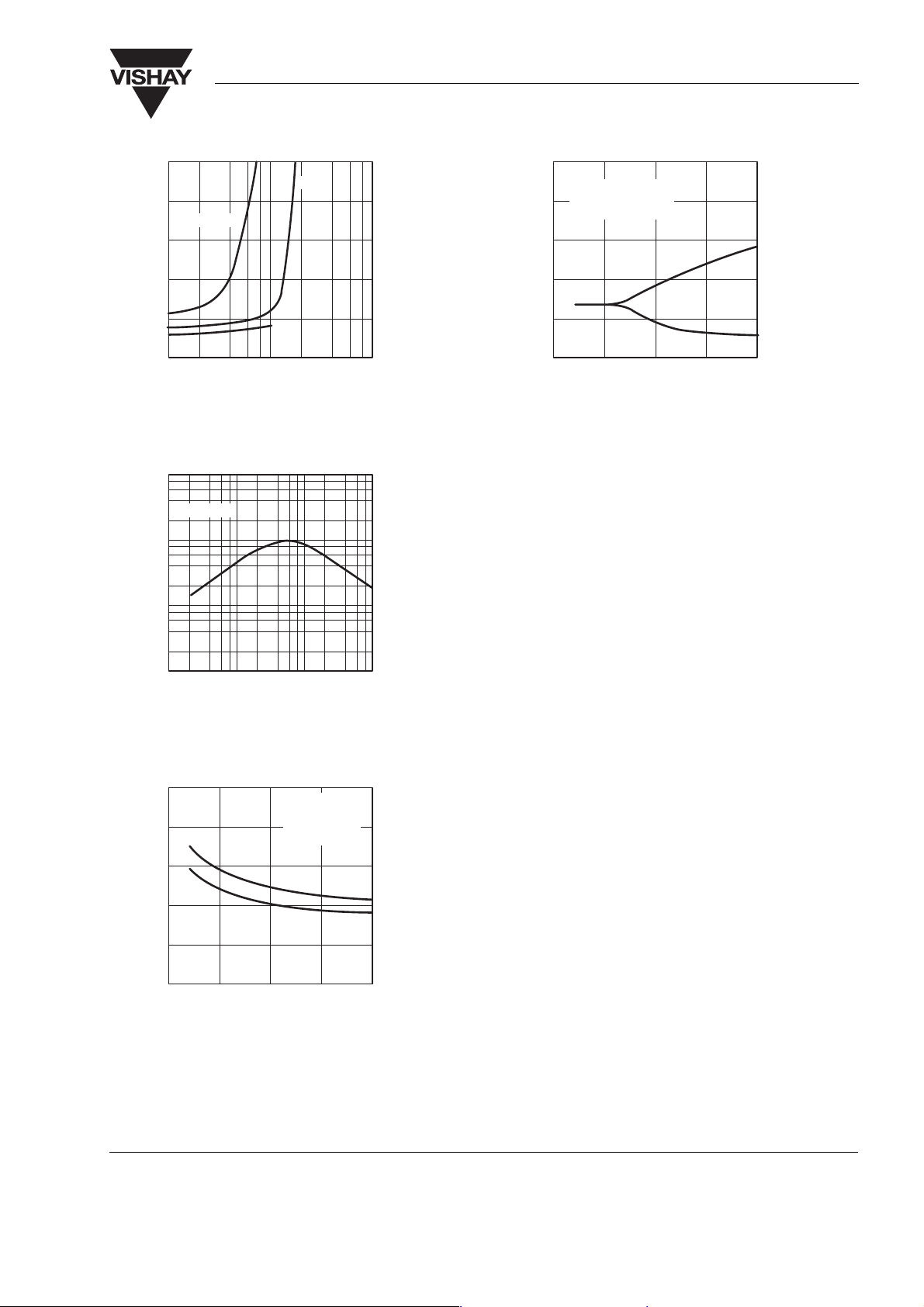
Figure 9. Collector Dark Current vs. Ambient Temperature
100
VCE=5V
10
1
1
F
I - Forward Current ( mA )
0.1
0 0.2 0.4 0.6 0.8 1.0 1.2 1.4 1.6 1.8 2.0
96 11862
VF- Forward Voltage(V)
Figure 7. Forward Current vs. Forward Voltage
2.0
=5V
V
CE
=5mA
I
F
1.5
1.0
0.5
rel
0
CTR – Relative Current Transfer Ratio
–25 0 25 50
T
95 11025
– Ambient Temperature ( °C )
amb
75
Figure 8. Relative Current Transfer Ratio vs. Ambient
Temperature
0.1
C
I – Collector Current ( mA)
0.01
0.1 1 10
95 11027
IF– Forward Current ( mA )
100
Figure 10. Collector Current vs. Forward Current
100
10
1
C
I – Collector Current ( mA)
0.1
0.1 1 10
95 10985
V
CE
IF=50mA
– Collector Emitter Voltage(V)
20mA
10mA
5mA
2mA
1mA
100
Figure 11. Collector Current vs. Collector Emitter Voltage
www.vishay.com
6
Document Number 83514
Rev. 1.8, 03-Dec-04
TCLT11.. Series
Vishay Semiconductors
1.0
20%
0.8
CTR=50%
0.6
0.4
CEsat
V – Collector Emitter Saturation Voltage (V)
95 11028
0.2
0
110
IC– Collector Current ( mA )
10%
100
Figure 12. Collector Emitter Saturation Voltage vs. Collector
Current
1000
VCE=5V
100
10
50
µ
Saturated Operation
V
S
40
R
L
=5V
=1k Ω
30
t
off
20
10
off
on
t /t –Turnon / Turnoff Time ( s )
0
t
on
0 5 10 15
I
95 11031
– Forward Current ( mA )
F
Figure 15. Turn on / off Time vs. Forward Current
20
CTR – Current Transfer Ratio ( % )
1
0.1 1 10
95 11029
IF– Forward Current ( mA )
100
Figure 13. Current Transfer Ratio vs. Forward Current
µ
off
on
t /t –Turnon / Turnoff Time ( s )
95 11030
10
8
t
on
6
t
off
4
2
0
02 4 6
I
– Collector Current ( mA )
C
Non Saturated
Operation
=5V
V
S
R
=100 Ω
L
10
Figure 14. Turn on / off Time vs. Collector Current
Document Number 83514
Rev. 1.8, 03-Dec-04
www.vishay.com
7

TCLT11.. Series
Vishay Semiconductors
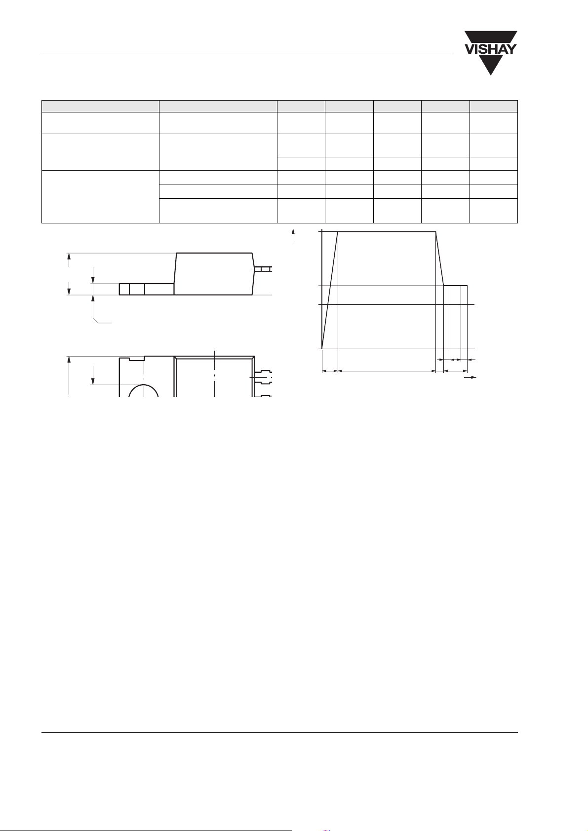
Package Dimensions in mm
www.vishay.com
8
15227
Document Number 83514
Rev. 1.8, 03-Dec-04

TCLT11.. Series
Vishay Semiconductors
Ozone Depleting Substances Policy Statement
It is the policy of Vishay Semiconductor GmbH to
1. Meet all present and future national and international statutory requirements.
2. Regularly and continuously improve the performance of our products, processes, distribution and
operatingsystems with respect to their impact on the health and safety of our employees and the public, as
well as their impact on the environment.
It is particular concern to control or eliminate releases of those substances into the atmosphere which are
known as ozone depleting substances (ODSs).
The Montreal Protocol (1987) and its London Amendments (1990) intend to severely restrict the use of ODSs
and forbid their use within the next ten years. Various national and international initiatives are pressing for an
earlier ban on these substances.
Vishay Semiconductor GmbH has been able to use its policy of continuous improvements to eliminate the use
of ODSs listed in the following documents.
1. Annex A, B and list of transitional substances of the Montreal Protocol and the London Amendments
respectively
2. Class I and II ozone depleting substances in the Clean Air Act Amendments of 1990 by the Environmental
Protection Agency (EPA) in the USA
3. Council Decision 88/540/EEC and 91/690/EEC Annex A, B and C (transitional substances) respectively.
Vishay Semiconductor GmbH can certify that our semiconductors are not manufactured with ozone depleting
substances and do not contain such substances.
We reserve the right to make changes to improve technical design
and may do so without further notice.
Parameters can vary in different applications. All operating parameters must be validated for each
customer application by the customer. Should the buyer use Vishay Semiconductors products for any
unintended or unauthorized application, the buyer shall indemnify Vishay Semiconductors against all
claims, costs, damages, and expenses, arising out of, directly or indirectly, any claim of personal
damage, injury or death associated with such unintended or unauthorized use.
Vishay Semiconductor GmbH, P.O.B. 3535, D-74025 Heilbronn, Germany
Telephone: 49 (0)7131 67 2831, Fax number: 49 (0)7131 67 2423
Document Number 83514
Rev. 1.8, 03-Dec-04
www.vishay.com
9
 Loading...