

Automotive
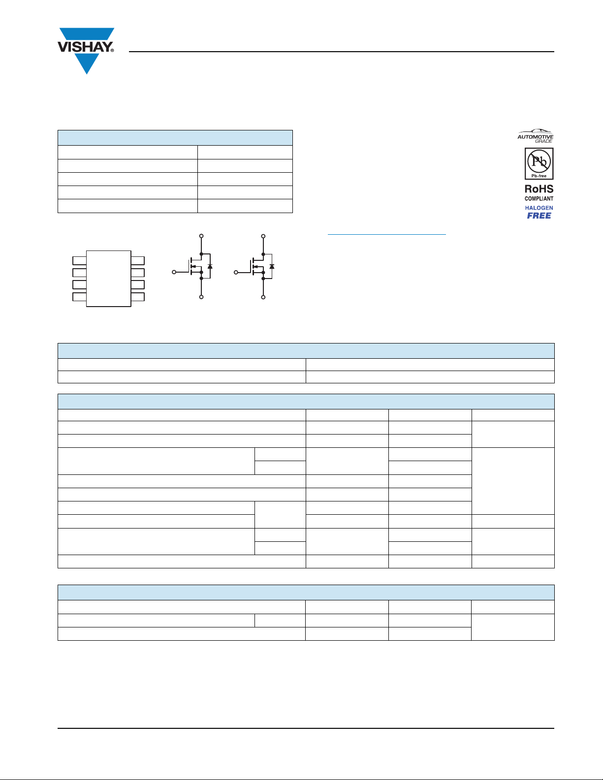
S
1
D
1
G
1
D
1
S
2
D
2
G
2
D
2
SO-8
5
6
7
8
Top View
2
3
4
1
Dual N-Channel 40 V (D-S) 175 °C MOSFET
SQ4940EY
Vishay Siliconix
PRODUCT SUMMARY
VDS (V) 40
R
() at VGS = 10 V 0.035
DS(on)
() at VGS = 4.5 V 0.055
R
DS(on)
(A) 7
I
D
Configuration Dual
FEATURES
• Halogen-free According to IEC 61249-2-21
Definition
•TrenchFET
• Compliant to RoHS Directive 2002/95/EC
• AEC-Q101 Qualified
• Find out more about Vishay’s Automotive
®
Power MOSFET
c
Grade Product Requirements at:
G
1
N-Channel MOSFET
D
1
G
2
S
1
D
2
S
2
N-Channel MOSFET
www.vishay.com/applications
ORDERING INFORMATION
Package SO-8
Lead (Pb)-free and Halogen-free SQ4940EY-T1-GE3
ABSOLUTE MAXIMUM RATINGS (TC = 25 °C, unless otherwise noted)
PARAMETER SYMBOL LIMIT UNIT
Drain-Source Voltage V
Gate-Source Voltage V
= 25 °C
T
Continuous Drain Current
C
T
= 125 °C 4
C
Continuous Source Current (Diode Conduction) I
Pulsed Drain Current
Single Pulse Avalanche Energy
Single Pulse Avalanche Current E
Maximum Power Dissipation
a
L = 0.1 mH
a
TC = 25 °C
T
= 125 °C 1.1
C
Operating Junction and Storage Temperature Range T
DS
± 20
GS
I
D
S
IDM 28
I
AS
AS
P
D
, T
J
stg
40
V
7
3
A
17
14 mJ
3.3
W
- 55 to + 175 °C
THERMAL RESISTANCE RATINGS
PARAMETER SYMBOL LIMIT UNIT
Junction-to-Ambient PCB Mount
Junction-to-Foot (Drain) R
Notes
a. Pulse test; pulse width 300 μs, duty cycle 2 %.
b. When mounted on 1" square PCB (FR-4 material).
c. Parametric verification ongoing.
Document Number: 72163 www.vishay.com
S10-2114-Rev. A, 27-Sep-10 1
b
R
thJA
thJF
110
45
°C/W
SQ4940EY
Vishay Siliconix
SPECIFICATIONS (TC = 25 °C, unless otherwise noted)
PARAMETER SYMBOL TEST CONDITIONS MIN. TYP. MAX. UNIT
Static
Drain-Source Breakdown Voltage V
Gate-Source Threshold Voltage V
Gate-Source Leakage I
Zero Gate Voltage Drain Current I
a
On-State Drain Current
Drain-Source On-State Resistance
Forward Transconductance
Dynamic
b
I
a
R
b
Input Capacitance C
Reverse Transfer Capacitance C
Total Gate Charge
Gate-Drain Charge
Turn-On Delay Time
Rise Time
c
Turn-Off Delay Time
Fall Time
c
c
c
c
c
c
Source-Drain Diode Ratings and Characteristics
Pulsed Current
a
Forward Voltage V
DS
GS(th)
V
GSS
DSS
V
D(on)
DS(on)
g
fs
iss
- 102 130
oss
-5265
rss
Qg
Qgs -2-
Qgd -2.9-
t
d(on)
t
r
t
-1928
d(off)
tf -711
b
I
SM
SD
Notes
a. Pulse test; pulse width 300 μs, duty cycle 2 %.
b. Guaranteed by design, not subject to production testing.
c. Independent of operating temperature.
V
VGS = 0 V, ID = 250 μA 40 - -
VDS = VGS, ID = 250 μA 1.5 2.0 2.5
= 0 V, VGS = ± 20 V - - ± 100 nA
DS
VGS = 0 V VDS = 40 V - - 1.0
= 0 V VDS = 40 V, TJ = 125 °C - - 50
GS
= 0 V VDS = 40 V, TJ = 175 °C - - 150
V
GS
= 10 V VDS5 V 25 - - A
GS
V
= 10 V ID = 6 A - 0.026 0.035
GS
= 10 V ID = 6 A, TJ = 125 °C - - 0.056
V
GS
V
= 10 V ID = 6 A, TJ = 175 °C - - 0.067
GS
= 4.5 V ID = 5 A - 0.035 0.055
GS
VDS = 15 V, ID = 6 A - 17 - S
- 663 830
V
= 0 V VDS = 25 V, f = 1 MHz
GS
-1421
= 10 V VDS = 20 V, ID = 5.7 A
V
GS
-812
= 20 V, RL = 20
V
DD
I
1 A, V
D
= 10 V, Rg = 1
GEN
-812
--28A
IF = 2 A, V
= 0 V - 0.8 1.1 V
GS
V
μA V
pF Output Capacitance C
nC Gate-Source Charge
ns
Stresses beyond those listed under “Absolute Maximum Ratings” may cause permanent damage to the device. These are stress ratings only, and functional operation
of the device at these or any other conditions beyond those indicated in the operational sections of the specifications is not implied. Exposure to absolute maximum
rating conditions for extended periods may affect device reliability.
www.vishay.com Document Number: 72163
2 S10-2114-Rev. A, 27-Sep-10
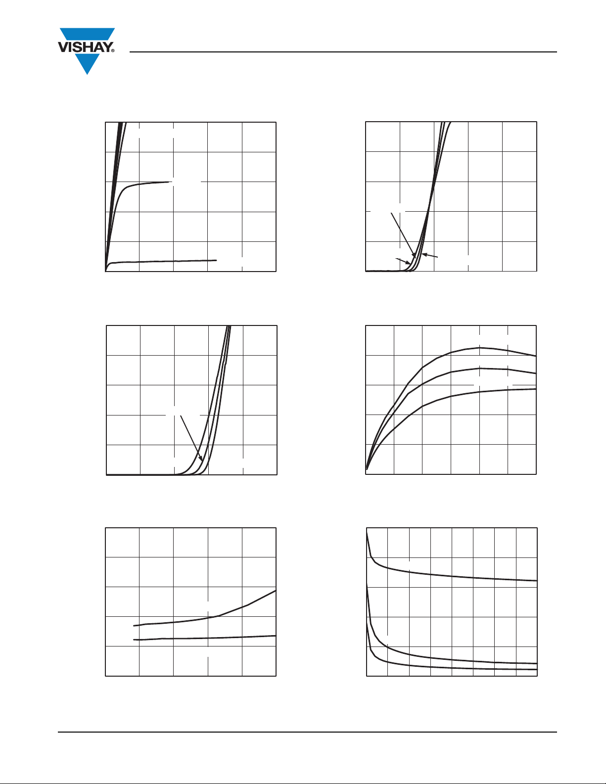
TYPICAL CHARACTERISTICS (TA = 25 °C, unless otherwise noted)
0
6
12
18
24
30
0 2 4 6 8 10
I
D
- Drain Current (A)
VDS-Drain-to-Source Voltage (V)
VGS= 10 V thru 5 V
VGS= 3 V
V
= 4 V
0
2
4
6
8
10
0 1 2 3 4 5
I
D
- Drain Current (A)
VGS- Gate-to-Source Voltage (V)
TC= 125 °C
TC= - 55 °C
TC= 25 °C
0.00
0.02
0.04
0.06
0.08
0.10
0 6 12 18 24 30
R
DS(on)
-On-Resistance (Ω)
ID-Drain Current (A)
VGS= 4.5 V
VGS= 10 V
0
6
12
18
24
30
0 2 4 6 8 10
I
D
- Drain Current (A)
VGS- Gate-to-Source Voltage (V)
TC= - 55 °C
TC= 125 °C
TC= 25 °C
0
200
400
600
800
1000
0 5 10 15 20 25 30 35 40
C - Capacitance (pF)
VDS-Drain-to-Source Voltage (V)
C
iss
C
oss
C
rss
SQ4940EY
Vishay Siliconix
Output Characteristics
Transfer Characteristics
Transfer Characteristics
25
TC= - 55 °C
20
15
10
-Transconductance (S)
fs
g
5
0
0 2 4 6 8 10 12
ID- Drain Current (A)
TC= 25 °C
TC= 125 °C
Transconductance
On-Resistance vs. Drain Current
Document Number: 72163 www.vishay.com
S10-2114-Rev. A, 27-Sep-10 3
Capacitance

SQ4940EY
0
2
4
6
8
10
0 3 6 9 12 15
V
GS
- Gate-to-Source Voltage (V)
Qg-Total Gate Charge (nC)
ID= 5.7 A
V
DS
= 20 V
0.001
0.01
0.1
1
10
100
0.0 0.2 0.4 0.6 0.8 1.0 1.2
I
S
- Source Current (A)
VSD- Source-to-Drain Voltage (V)
TJ= 25 °C
TJ= 150 °C
-1.0
-0.7
-0.4
-0.1
0.2
0.5
- 50 - 25 0 25 50 75 100 125 150 175
V
GS(th)
Variance (V)
TJ-Temperature (°C)
I
= 250 μA
I
= 5 mA
Vishay Siliconix
TYPICAL CHARACTERISTICS (TA = 25 °C, unless otherwise noted)
2.0
Gate Charge
ID= 5.7 A
1.7
1.4
-On-Resistance
1.1
(Normalized)
DS(on)
R
0.8
0.5
- 50 - 25 0 25 50 75 100 125 150 175
TJ- Junction Temperature (°C)
VGS= 10 V
VGS= 4.5 V
On-Resistance vs. Junction Temperature
0.15
0.12
0.09
0.06
-On-Resistance (Ω)
DS(on)
R
0.03
TJ= 25 °C
TJ= 150 °C
Source Drain Diode Forward Voltage
Threshold Voltage
www.vishay.com Document Number: 72163
4 S10-2114-Rev. A, 27-Sep-10
0.00
0246810
VGS- Gate-to-Source Voltage (V)
On-Resistance vs. Gate-to-Source Voltage
52
50
48
46
-Drain-to-Source Voltage (V)
DS
44
V
42
- 50 - 25 0 25 50 75 100 125 150 175
ID= 1 mA
TJ- Junction Temperature (°C)
Drain Source Breakdown vs. Junction Temperature

THERMAL RATINGS (TA = 25 °C, unless otherwise noted)
0.01
0.1
1
10
100
0.01 0.1 1 10 100
I
D
- Drain Current (A)
VDS-Drain-to-Source Voltage (V)
* V
GS
> minimum VGSat which R
DS(on)
is specied
100 ms
Limited by R
DS(on)
*
1 ms
IDMLimited
TC= 25 °C
Single Pulse
BVDSS Limited
10 ms
100 μs
1 s
10 s, DC
2
1
0.1
0.01
10
-4
10
-3
10
-2
10
-1
1 10 600
0.2
0.1
0.05
0.02
Single Pulse
Duty Cycle = 0.5
Square Wave Pulse Duration (s)
Normalized Effective Transient
Thermal Impedance
1. Duty Cycle, D =
2. Per Unit Base = R
thJA
= 110 °C/W
3. T
JM
- TA = PDMZ
thJA
(t)
t
1
t
2
t
1
t
2
Notes:
4. Surface Mounted
P
DM
100
Safe Operating Area
SQ4940EY
Vishay Siliconix
Document Number: 72163 www.vishay.com
S10-2114-Rev. A, 27-Sep-10 5
Normalized Thermal Transient Impedance, Junction-to-Ambient

SQ4940EY
Vishay Siliconix
THERMAL RATINGS (TA = 25 °C, unless otherwise noted)
2
1
Duty Cycle = 0.5
0.2
0.1
0.1
Thermal Impedance
Normalized Effective Transient
0.05
0.02
Single Pulse
0.01
-4
10
-3
10
-2
10
Square Wave Pulse Duration (s)
10
-1
110
Normalized Thermal Transient Impedance, Junction-to-Foot
Note
• The characteristics shown in the two graphs
- Normalized Transient Thermal Impedance Junction-to-Ambient (25 °C)
- Normalized Transient Thermal Impedance Junction-to-Foot (25 °C)
are given for general guidelines only to enable the user to get a “ball park” indication of part capabilities. The data are extracted from single
pulse transient thermal impedance characteristics which are developed from empirical measurements. The latter is valid for the part
mounted on printed circuit board - FR4, size 1" x 1" x 0.062", double sided with 2 oz. copper, 100 % on both sides. The part capabilities
can widely vary depending on actual application parameters and operating conditions.
Vishay Siliconix maintains worldwide manufacturing capability. Products may be manufactured at one of several qualified locations. Reliability data for Silicon
Technology and Package Reliability represent a composite of all qualified locations. For related documents such as package/tape drawings, part marking, and
reliability data, see www.vishay.com/ppg?72163
.
www.vishay.com Document Number: 72163
6 S10-2114-Rev. A, 27-Sep-10

Legal Disclaimer Notice
Vishay
Disclaimer
ALL PRODUCT, PRODUCT SPECIFICATIONS AND DATA ARE SUBJECT TO CHANGE WITHOUT NOTICE TO IMPROVE
RELIABILITY, FUNCTION OR DESIGN OR OTHERWISE.
Vishay Intertechnology, Inc., its affiliates, agents, and employees, and all persons acting on its or their behalf (collectively,
“Vishay”), disclaim any and all liability for any errors, inaccuracies or incompleteness contained in any datasheet or in any other
disclosure relating to any product.
Vishay makes no warranty, representation or guarantee regarding the suitability of the products for any particular purpose or
the continuing production of any product. To the maximum extent permitted by applicable law, Vishay disclaims (i) any and all
liability arising out of the application or use of any product, (ii) any and all liability, including without limitation special,
consequential or incidental damages, and (iii) any and all implied warranties, including warranties of fitness for particular
purpose, non-infringement and merchantability.
Statements regarding the suitability of products for certain types of applications are based on Vishay’s knowledge of typical
requirements that are often placed on Vishay products in generic applications. Such statements are not binding statements
about the suitability of products for a particular application. It is the customer’s responsibility to validate that a particular
product with the properties described in the product specification is suitable for use in a particular application. Parameters
provided in datasheets and/or specifications may vary in different applications and performance may vary over time. All
operating parameters, including typical parameters, must be validated for each customer application by the customer’s
technical experts. Product specifications do not expand or otherwise modify Vishay’s terms and conditions of purchase,
including but not limited to the warranty expressed therein.
Except as expressly indicated in writing, Vishay products are not designed for use in medical, life-saving, or life-sustaining
applications or for any other application in which the failure of the Vishay product could result in personal injury or death.
Customers using or selling Vishay products not expressly indicated for use in such applications do so at their own risk and agree
to fully indemnify and hold Vishay and its distributors harmless from and against any and all claims, liabilities, expenses and
damages arising or resulting in connection with such use or sale, including attorneys fees, even if such claim alleges that Vishay
or its distributor was negligent regarding the design or manufacture of the part. Please contact authorized Vishay personnel to
obtain written terms and conditions regarding products designed for such applications.
No license, express or implied, by estoppel or otherwise, to any intellectual property rights is granted by this document or by
any conduct of Vishay. Product names and markings noted herein may be trademarks of their respective owners.
Document Number: 91000 www.vishay.com
Revision: 11-Mar-11 1

 Loading...