

Page 1

SPX5205
150mA, LOW-NOISE LDO VOLTAGE REGULATOR
JULY 30, 2008 REV. H
FEATURES
■ Low Noise Output LDO: 40μV
■ 1% Initial Accuracy
■ Very Low Quiecent Current: 70μA
■ Low Dropout Voltage (210mV at 150mA)
■ Current and Thermal Limiting
■ Reverse-Battery Protection
■ Wide Range of Fix Output Voltages:1.2V, 1.5V,
1.8V, 2.0V, 2.5V, 2.8V, 3.0V, 3.3V and 5.0V
■ Zero Off-Mode Current
RMS
Possible
Fixed Output Voltage
V
OUT
54
BYP
SPX5205
5 Pin SOT-23
123
V
IN
Adjustable Output Voltage
V
OUT
54
GND
EN
ADJ/BYP
■ Small 5-Pin SOT-23
■ Pin Compatible to MIC5205/MAX8877
(fixed Options Only) and AS3815
SPX5205
5 Pin SOT-23
123
V
IN
GND
EN
APPLICATIONS
■ PDA
■ Battery Powered Systems
■ Cellular Phone
■ Cordless Telephones
■ Radio Control Systems
■ Laptop, Palmtop, and Notebook Computers
Now Available in Lead Free Packaging
■ Portable Consumer Equipment
■ Portable Instrumentation
■ Bar Code Scanners
■ SMPS Post-Regulator
DESCRIPTION
The SPX5205 is a positive voltage regulator with very low dropout voltage, output noise and ground current
(750μA at 100mA). V
voltages 1.2V, 1.5V, 1.8V, 2.0V, 2.5V, 2.8V, 3.0V, 3.3V, and 5.0V and an adjustable version are available
in a small 5-pin SOT-23 package. Other key features include zero off-mode current, reverse battery
protection, thermal shutdown and current limit. The SPX5205 is an excellent choice for use in batterypowered applications, and where powe
control systems, and portable computers.
has a tolerance of less than 1% and is temperature compensated. Fixed output
OUT
r conservation is desired such as: cellular/ cordless telephones, radio
TYPICAL APPLICATION CIRCUIT
V
IN
GND
+
EN
ENABLE may be tied directly to V
1
2
5
+
1.0μF
V
OUT
SPX5205
3
4
BYP
(Optn)
IN
TOP View
Exar Corporation 48720 Kato Road, Fremont CA, 94538 • (510) 668-7000 • FAX (510) 668-7017 • www.exar.com
Page 2
SPX5205
VIN = VOUT + 1V ≥ 2.5V
1.0 IL = 100uA to 1mA
VIN = VOUT +1 to 16V and VEN ≤ 6V
VIN = VEN =VOUT +1 ≤ 8V
0.2 %/V
VIN = VEN =VOUT +1 to 16V
Ta = 25°C to 85°C
150mA, Low-Noise LDO Voltage Regulator REV. H
ABSOLUTE MAXIMUM RATINGS
Thermal Shutdown .................................................................... Internally Limited
Lead Temperature (Soldering, 5 seconds) ................................................. 260°C
Operating Junction Temperature Range .................................... -40°C to +125°C
RECOMMENDED OPERATING CONDITIONS
Input voltage ..................................................................................... +2.5V to 16V
Operating Junction Temperature Range .................................... -40°C to +125°C
Enable Input Voltage .............................................................................. 0V to V
SOT-23-5 (eJA) ................................................................................... See Note 1
TJ=25°C, VIN = V
apply over full temperature range -40°C to +85°C, unless otherwise specified.
+ 1V, IL = 100μA, CL = 1μF, and V
OUT
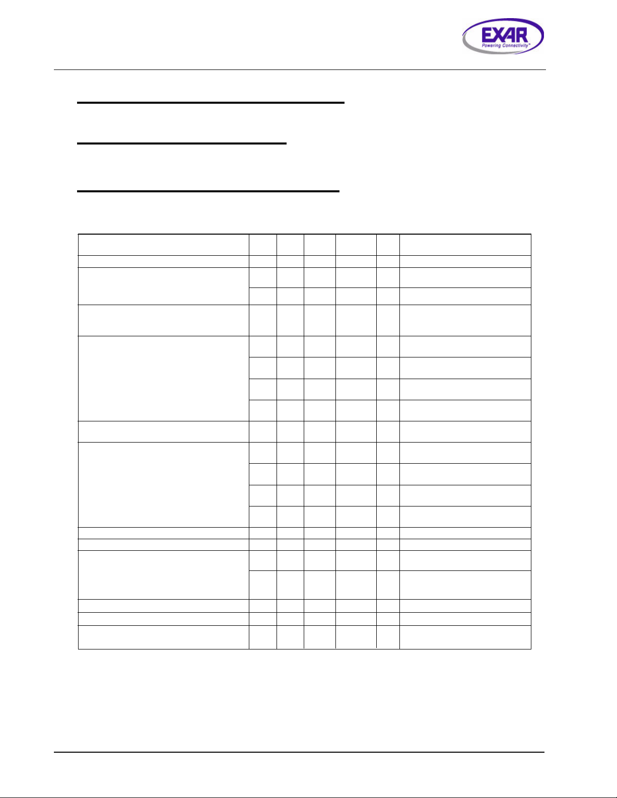
PARAMETER MIN TYP MAX UNITS CONDITIONS
Output Voltage Tolerance (V
) -1 +1 %V
OUT
-2 +2 z
Output Voltage Temperature Coefficient 57 ppm/°C z
Line Regulation 0.03 0.1 %/V
IN
ENABLE
0.2 z
Input Supply Voltage ......................................... -20V to +20V
Enable Input Voltage ......................................... -20V to +20V
ELECTRICAL CHARACTERISTICS
* 2.4V. The z denotes the specifications which
NOM
Load Regulation 0.1 0.2 %
0.5 z IL = 1mA to 150mA
z
Dropout Voltage (See Note 2) 30 50 mV IL = 100μA
(V
- VO) 70 z
IN
140 190 mV IL = 50mA
230 z
180 250 mV IL = 100mA
300 z
210 275 mV IL = 150mA
350 z
Quiescent Current (I
) 0.05 1 μA V
GND
5 z V
ENABLE
ENABLE
) 0.4V
) 0.25V
Ground Pin Current 70 125 μA IL = 100μA
) 150 z
(I
GND
350 600 IL = 50mA
800 z
750 1000 IL = 100mA
1500 z
1300 1900 IL = 150mA
2500 z
Ripple Rejection (PSRR) 70 dB
Current Limit (I
Output Noise (eNO) 300 μV
) 360 500 mA V
LIMIT
RMS
40 μV
RMS
= 0V
OUT
IL = 10mA, CL = 1μF, CIN= 1μF
(10Hz - 100kHz.)
IL = 10mA, CL = 10μF, C
1μF,C
=1μF,(10Hz - 100kHz)
IN
BYP
=
Input Voltage Level Logic Low (VIL) 0.4 V OFF
Input Voltage Level Logic High (VIL) 2.0 ON
ENABLE Input Current 0.01 2 μA VIL ) 0.4V
Note 1: The maximum allowable power dissipation is a function of maximum operating junction temperature, T
resistance, and the ambient, eJ
given: P
D (max)
regulator will go into thermal shutdown. The eJ
Note 2: Not applicable to output voltages of less than 2V.
= (T
3 20 V
, and the ambient temperature TA. The maximum allowable power dissipation at any ambient temperature is
A
- TA)/eJA, exceeding the maximum allowable power limit will result in excessive die temperature; thus, the
J (max)
of the SPX5205 is 220°C/W mounted on a PC board.
A
* 2.0V
IH
J (max)
2
, the junction to ambient thermal
Page 3

SPX5205
REV. H 150mA, Low-Noise LDO Voltage Regulator
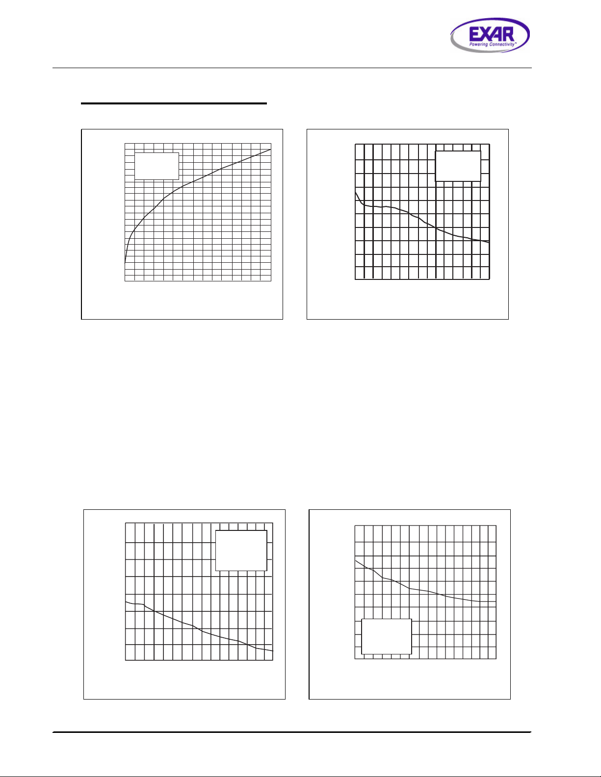
TYPICAL PERFORMANCE CHARACTERISTICS
1.40
1.20
1.00
0.80
(mA)
0.60
GND
I
0.40
0.20
0.00
3.3V Device
VIN= 3.2V
= 1.0μF
C
L
0 50 100 150
IL (mA)
Ground Current vs Load Current
110
100
90
80
(μA)
70
GND
I
60
50
40
30
4 6 8 10 12 14 16
Ground Current vs Input Voltage
VO = 3.3V
C
IL = 100μA
VIN (V)
= 1.0μF
L
2.00
3.3V Device
= 4.3V
V
IN
CL = 1.0μF
1.50
(mA)
1.00
GND
I
0.50
0.00
0 50 100 150
IL (mA)
Ground Current vs Load Current in Dropout
3.340
3.335
3.330
3.325
(V)
3.320
3.315
OUT
V
3.310
3.305
3.300
3.295
3.290
4 6 8 10 12 14 16
Output Voltage vs Input Voltage
3
VIN (V)
3.3V Device
CL= 1.0μF
I
= 100μA
L
Page 4
SPX5205
150mA, Low-Noise LDO Voltage Regulator REV. H
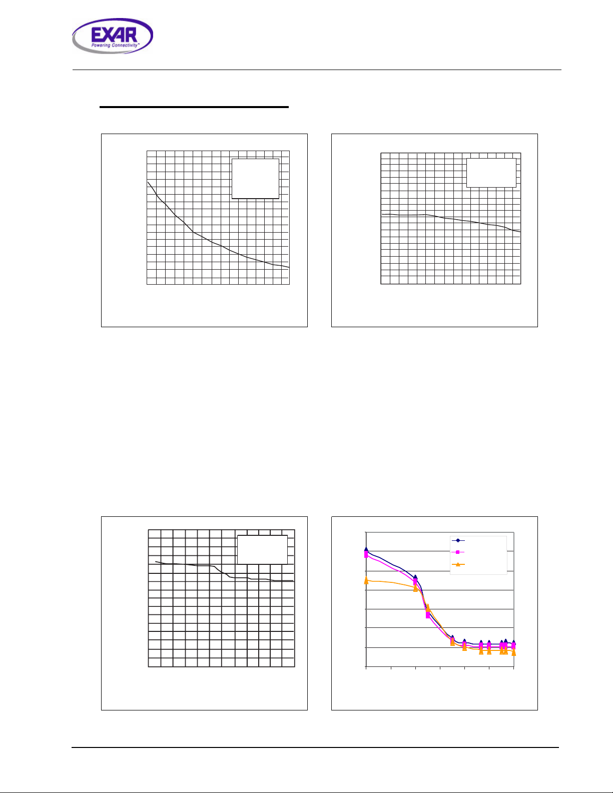
TYPICAL PERFORMANCE CHARACTERISTICS
3.310
200
VO=3.3V
V
= 3.2V
IN
CL = 1.0μF
150
100
Dropout (mV)
(V)
OUT
V
3.308
3.306
3.304
3.3V Device
VIN= 4.3V
CL = 1.0μF
50
0
0 50 100 150
IL (mA)
Dropout Voltage vs Load Current
90.0
80.0
(μA)
70.0
GND
I
60.0
50.0
-40 -20 0 20 40 60 80 100 120
Temperature (°C)
V
= 3.3V
OUT
V
= 4.3V
IN
CL= 1.0μF
= 100μA
I
L
3.302
3.300
0 50 100 150
Output Voltage vs Load Current
950
850
750
(μA)
650
GND
I
V
= 3.3V
550
450
OUT
= 4.3V
V
IN
CL= 1.0μF
IL = 100mA
-40 -20 0 20 40 60 80 100 120
Temperature (°C)
IL (mA)
Ground Current vs Temperature at I
LOAD
=100μA
Ground Current vs Temperature at I
4
4
LOAD
=100mA
Page 5
SPX5205
REV. H 150mA, Low-Noise LDO Voltage Regulator
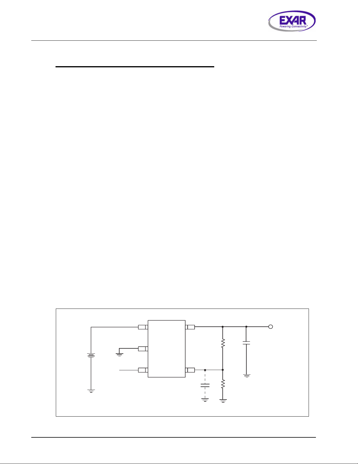
TYPICAL PERFORMANCE CHARACTERISTICS
2.30
2.20
2.10
2.00
1.90
(mA)
1.80
GND
I
1.70
1.60
1.50
1.40
-40 -20 0 20 40 60 80 100 120
V
OUT
V
IN
C
L
= 150mA
I
L
Temperature (°C)
Ground Current in Dropout vs Temperature
= 3.3V
= 4.3V
= 1.0μF
3.400
3.380
3.360
3.340
3.320
(V)
3.300
OUT
3.280
V
3.260
3.240
3.220
3.200
-40 -20 0 20 40 60 80 100 120
Temperature (°C)
Output Voltage vs Temperature
V
= 3.3V
OUT
= 4.3V
V
IN
CL= 1.0μF
1.60
V
=3.3V
OUT
= 1.0μA
C
L
I
= 100μA
L
(V)
1.50
1.40
1.30
1.20
1.10
On Threshold
1.00
EN,
V
0.90
0.80
4 6 8 10 12 14 16
VIN (V)
ENABLE Voltage, ON threshold vs Input Voltage
350
300
250
200
150
uV RMS
100
50
0
1 10 100 1000 10000 100000 1000000
Bypass Cap (pF)
Output Noise vs. Bypass Capacitor Value
5
Cin = 1uFT,
Cout = 1uFT
Cin = 1uFT,
Cout = 2.2uFT
Cin = 1uFT
Cout = 10uFT
Page 6
SPX5205
150mA, Low-Noise LDO Voltage Regulator REV. H
APPLICATION INFORMATION
The SPX5205 requires an output capacitor for
device stability. Its value depends upon the
application circuit. In general, linear regulator
stability decreases with higher output currents.
In applications where the SPX5205 is putting
out less current, a lower output capacitance may
be sufficient. For example, a regulator sourcing
only 10mA, requires approximately half the
capacitance as the same regulator sourcing
150mA.
Bench testing is the best method for determining
the proper type and value of the capacitor since
the high frequency characteristics of electrolytic capacitors vary widely, depending on type
and manufacturer. A high quality 2.2μF aluminum electrolytic capacitor works in most application circuits, but the same stability often can
be obtained with a 1μF tantalum electrolytic.
With the SPX5205 adjustable version, the minimum value of output capacitance is a function of
the output voltage. The value decreases with
higher output voltages, since closed loop gain is
increased.
Typical Applications Circuits
A 10nF capacitor on BYP pin will significantly
reduce output noise but it may be left unconnected if the output noise is not a major concern.
The SPX5205 start-up speed is inversely pro-
portional to the size of the BYP capacitor. Applications requiring a slow ramp-up of the output voltage should use a larger C
. However,
BYP
if a rapid turn-on is necessary, the BYP capacitor can be omitted.
The SPX5205’s internal reference is available
through the BYP pin.
The Typical Application Circuit shown on page
1 represents a SPX5205 standard application
circuit. The EN (enable) pin is pulled high
(>2.0V) to enable the regulator. To disable the
regulator, EN < 0.4V.
The SPX5205 in Figure 1 illustrates a typical
adjustable output voltage configuration. Two
resistors (R1 and R2) set the output voltage. The
output voltage is calculated using the formula:
= 1.235V x ( 1 + R1/R2)
V
OUT
R2 must be > 10 k1 and for best results, R2
should be between 22 k1 and 47k1. A capacitor
placed between adjustable and ground will provide improved noise performance.
V
IN
GND
+
EN
Hi-ON
Lo-OFF
Figure 1. Typical Adjustable Output Voltage.
1
2
3
SPX5205
TOP View
6
BYP
(Optn)
5
R1
4
ADJ
R2
+
V
OUT
Page 7
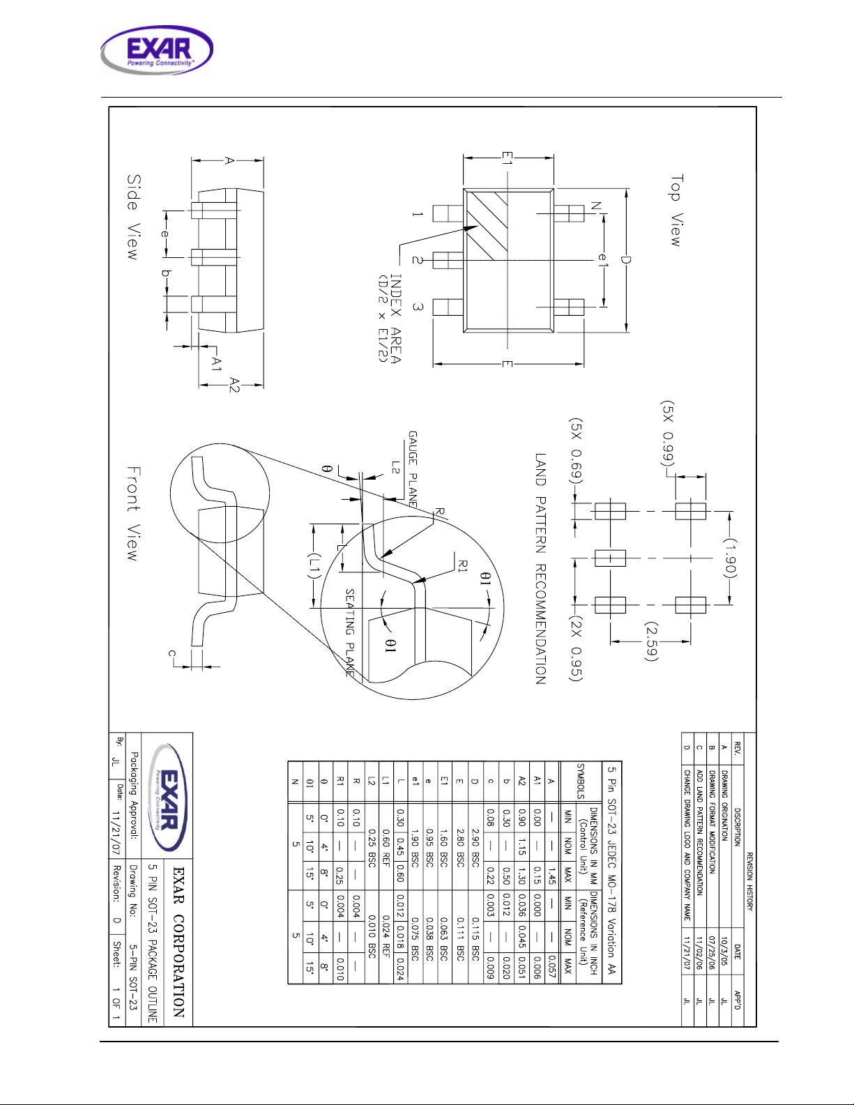
SPX5205
REV. H 150mA, Low-Noise LDO Voltage Regulator
7
Page 8
SPX5205
150mA, Low-Noise LDO Voltage Regulator REV. H
ORDERING INFORMATION
PART NUMBER TOP MARK ACC. OUTPUT VOLTAGE PACKAGE
SPX5205M5-L.............. H1WW ................. 1% ...................... Adj ................... 5 Pin SOT-23
SPX5205M5-L/TR ........ H1WW .................
SPX5205M5-L-1-2 ......... R12 ................... 1% ..................... 1.2V .................. 5 Pin SOT-23
SPX5205M5-L-1-2/TR
SPX5205M5-L-1-5 ......... R15 ................... 1% ..................... 1.5V .................. 5 Pin SOT-23
SPX5205M5-L-1-5/TR .... R15 ................... 1% ..................... 1.5V .................. 5 Pin SOT-23
SPX5205M5-L-1-8 ......... R18 ................... 1% ..................... 1.8V .................. 5 Pin SOT-23
SPX5205M5-L-1-8/TR .... R18 ................... 1% ..................... 1.8V .................. 5 Pin SOT-23
SPX5205M5-L-2-0 ......... R20 ................... 1% ..................... 2.0V .................. 5 Pin SOT-23
SPX5205M5-L-2-0/TR .... R20 ................... 1% ..................... 2.0V .................. 5 Pin SOT-23
SPX5205M5-L-2-5 ......... R25 ................... 1% ..................... 2.5V .................. 5 Pin SOT-23
SPX5205M5-L-2-5/TR .... R25 ................... 1% ..................... 2.5V .................. 5 Pin SOT-23
SPX5205M5-L-2-8 ......... R28 ................... 1%......................2.8V................... 5 Pin SOT-23
SPX5205M5-L-2-8/TR .... R28 ................... 1%......................2.8V................... 5 Pin SOT-23
SPX5205M5-L-3-0...........R30.....................1% .....................3.0V................... 5 PIN SOT-23
SPX5205M5-L-3-0/TR.....R30.....................1% .....................3.0V................... 5 PIN SOT-23
SPX5205M5-L-3-3 ......... R33 ................... 1% ..................... 3.3V .................. 5 Pin SOT-23
SPX5205M5-L-3-3/TR .... R33 ................... 1% ..................... 3.3V .................. 5 Pin SOT-23
SPX5205M5-L-5-0 ......... R50 ................... 1% ..................... 5.0V .................. 5 Pin SOT-23
SPX5205M5-L-5-0/TR .... R50 ................... 1% ..................... 5.0V .................. 5 Pin SOT-23
.... R12 ................... 1% ..................... 1.2V .................. 5 Pin SOT-23
1% ...................... Adj ................... 5 Pin SOT-23
All Packaging is lead free. A bar is added to indicate lead-free parts and can be mistaken as a “1” or an “I”.
/TR = Tape and Reel. Pack quantity is 2,500 for 5pin SOT-23
EXAR Technical Documentation: http://www.exar.com/TechDoc/default.aspx?
Exar Corporation
Headquarters and
Sales Office
48720 Kato Road
Fremont, CA 94538
main: 510-668-7000
fax: 510-668-7030
EXAR Corporation reserves the right to make changes to the products contained in this publication in
order to improve design, performance or reliability. EXAR Corporation assumes no responsibility for the
use of any circuits described herein, conveys no license under any patent or other right, and makes no
representation that the circuits are free of patent infringement. Charts and schedules contained here in
are only for illustration purposes and may vary depending upon a user’s specific application. While the
information in this publication has been carefully checked; no responsibility, however, is assumed for
inaccuracies.
EXAR Corporation does not recommend the use of any of its products in life support applications where
the failure or malfunction of the product can reasonably be expected to cause failure of the life support
system or to significantly affect its safety or effectiveness. Products are not authorized for use in such
applications unless EXAR Corporation receives, in writing, assurances to its satisfaction that: (a) the risk
of injury or damage has been minimized; (b) the user assumes all such risks; (c) potential liability of
EXAR Corporation is adequately protected under the circumstances.
8
 Loading...