

www.vishay.com
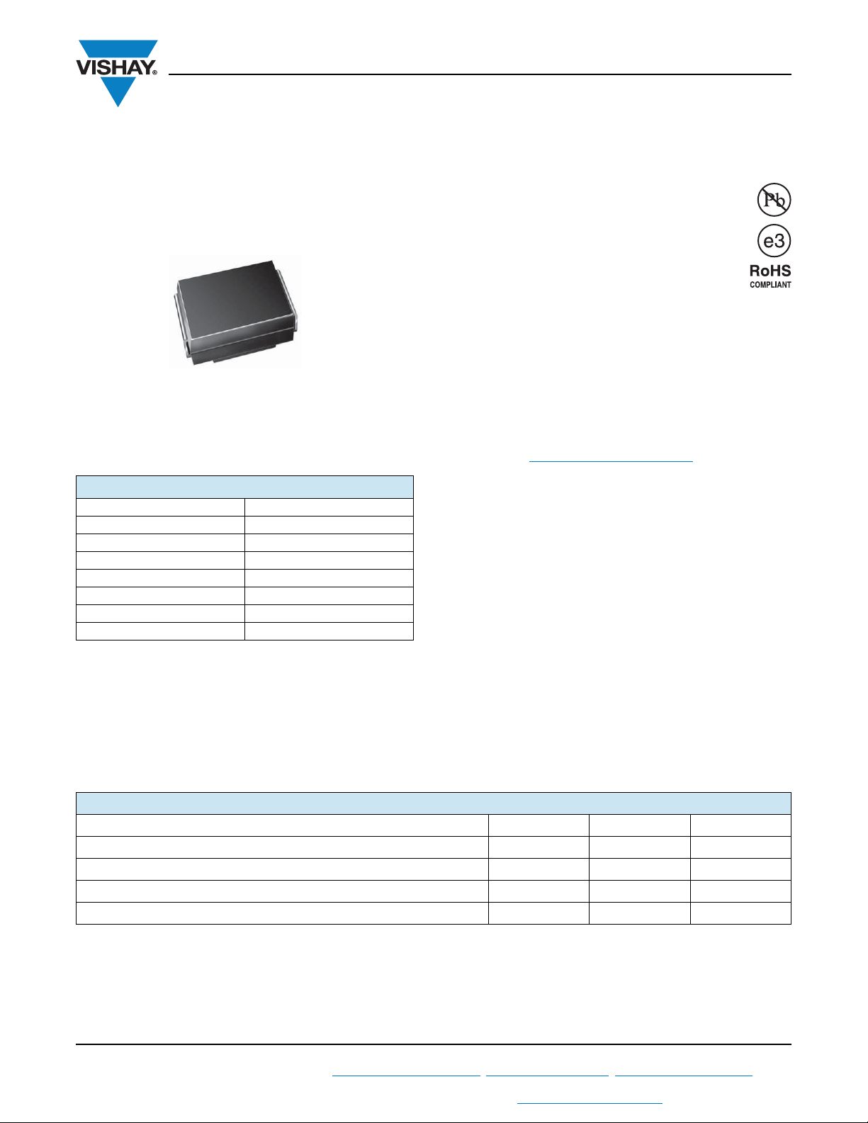
DO-214AA (SMB J-Bend)
SMBJ5.0A thru SMBJ188A
Vishay General Semiconductor
Surface Mount TRANSZORB®
Transient Voltage Suppressors
FEATURES
• Low profile package
• Ideal for automated placement
• Glass passivated chip junction
• Available in uni-directional and bi-directional
• 600 W peak pulse power capability with a
10/1000 μs waveform, repetitive rate (duty
cycle): 0.01 %
• Excellent clamping capability
• Very fast response time
• Low incremental surge resistance
• Meets MSL level 1, per J-STD-020, LF maximum peak of
260 °C
• AEC-Q101 qualified
• Material categorization: For definitions of compliance
please see www.vishay.com/doc?99912
PRIMARY CHARACTERISTICS
VBR (bi-directional) 6.4 V to 231 V
V
(uni-directional) 6.4 V to 231 V
BR
V
WM
P
PPM
I
(uni-directional only) 100 A
FSM
T
max. 150 °C
J
Polarity Uni-directional, bi-directional
Package DO-214AA (SMBJ)
5.0 V to 188 V
600 W
TYPICAL APPLICATIONS
Use in sensitive electronics protection against voltage
transients induced by inductive load switching and lighting
on ICs, MOSFET, signal lines of sensor units for consumer,
computer, industrial, and telecommunication.
MECHANICAL DATA
Case: DO-214AA (SMBJ)
Molding compound meets UL 94 V-0 flammability rating
Base P/N-E3 - RoHS-compliant, commercial grade
Base P/NHE3 - RoHS-compliant, AEC-Q101 qualified
Terminals: Matte tin plated leads, solderable per
J-STD-002 and JESD 22-B102
DEVICES FOR BI-DIRECTION APPLICATIONS
For bi-directional devices use CA suffix (e.g. SMBJ10CA).
Electrical characteristics apply in both directions.
E3 suffix meets JESD 201 class 1A whisker test, HE3 suffix
meets JESD 201 class 2 whisker test
Polarity: For uni-directional types the band denotes
cathode end, no marking on bi-directional types
MAXIMUM RATINGS (TA = 25 °C unless otherwise noted)
PARAMETER SYMBOL VALUE UNIT
Peak pulse power dissipation with a 10/1000 μs waveform
Peak pulse current with a 10/1000 μs waveform
Peak forward surge current 8.3 ms single half sine-wave uni-directional only
Operating junction and storage temperature range T
Notes
(1)
Non-repetitive current pulse, per fig. 3 and derated above TA = 25 °C per fig. 2.
(2)
Mounted on 0.2" x 0.2" (5.0 mm x 5.0 mm) copper pads to each terminal
(1)
(1)(2)
(fig. 1) P
(2)
PPM
I
See next table A
PPM
I
100 A
FSM
, T
- 55 to + 150 °C
J
STG
600 W
Revision: 10-Dec-12
For technical questions within your region: DiodesAmericas@vishay.com
THIS DOCUMENT IS SUBJECT TO CHANGE WITHOUT NOTICE. THE PRODUCTS DESCRIBED HEREIN AND THIS DOCUMENT
1
, DiodesAsia@vishay.com, DiodesEurope@vishay.com
ARE SUBJECT TO SPECIFIC DISCLAIMERS, SET FORTH AT www.vishay.com/doc?91000
Document Number: 88392
SMBJ5.0A thru SMBJ188A
www.vishay.com
ELECTRICAL CHARACTERISTICS (TA = 25 °C unless otherwise noted)
DEVICE TYPE
MODIFIED
DEVICE MARKING
CODE
“J” BEND LEAD
(+)
SMBJ5.0A
(+)
SMBJ6.0A KG KG 6.67 7.37 10 6.0 800 58.3 10.3
(+)
SMBJ6.5A KK AK 7.22 7.98 10 6.5 500 53.6 11.2
(+)
SMBJ7.0A KM KM 7.78 8.60 10 7.0 200 50.0 12.0
(+)
SMBJ7.5A KP AP 8.33 9.21 1.0 7.5 100 46.5 12.9
(+)
SMBJ8.0A KR AR 8.89 9.83 1.0 8.0 50 44.1 13.6
(+)
SMBJ8.5A KT AT 9.44 10.4 1.0 8.5 20 41.7 14.4
(+)
SMBJ9.0A KV AV 10.0 11.1 1.0 9.0 10 39.0 15.4
(+)
SMBJ10A KX AX 11.1 12.3 1.0 10 5.0 35.3 17.0
(+)
SMBJ11A KZ KZ 12.2 13.5 1.0 11 5.0 33.0 18.2
(+)
SMBJ12A LE BE 13.3 14.7 1.0 12 5.0 30.2 19.9
(+)
SMBJ13A LG LG 14.4 15.9 1.0 13 1.0 27.9 21.5
(+)
SMBJ14A LK BK 15.6 17.2 1.0 14 1.0 25.9 23.2
(+)
SMBJ15A LM BM 16.7 18.5 1.0 15 1.0 24.6 24.4
(+)
SMBJ16A LP LM 17.8 19.7 1.0 16 1.0 23.1 26.0
(+)
SMBJ17A LR LR 18.9 20.9 1.0 17 1.0 21.7 27.6
(+)
SMBJ18A LT BT 20.0 22.1 1.0 18 1.0 20.5 29.2
(+)
SMBJ20A LV LV 22.2 24.5 1.0 20 1.0 18.5 32.4
(+)
SMBJ22A LX BX 24.4 26.9 1.0 22 1.0 16.9 35.5
(+)
SMBJ24A LZ BZ 26.7 29.5 1.0 24 1.0 15.4 38.9
(+)
SMBJ26A ME CE 28.9 31.9 1.0 26 1.0 14.3 42.1
(+)
SMBJ28A MG MG 31.1 34.4 1.0 28 1.0 13.2 45.4
(+)
SMBJ30A MK CK 33.3 36.8 1.0 30 1.0 12.4 48.4
(+)
SMBJ33A MM CM 36.7 40.6 1.0 33 1.0 11.3 53.3
(+)
SMBJ36A MP CP 40.0 44.2 1.0 36 1.0 10.3 58.1
(+)
SMBJ40A MR CR 44.4 49.1 1.0 40 1.0 9.3 64.5
(+)
SMBJ43A MT CT 47.8 52.8 1.0 43 1.0 8.6 69.4
(+)
SMBJ45A MV MV 50.0 55.3 1.0 45 1.0 8.3 72.7
(+)
SMBJ48A MX MX 53.3 58.9 1.0 48 1.0 7.8 77.4
(+)
SMBJ51A MZ MZ 56.7 62.7 1.0 51 1.0 7.3 82.4
(+)
SMBJ54A NE NE 60.0 66.3 1.0 54 1.0 6.9 87.1
(+)
SMBJ58A NG NG 64.4 71.2 1.0 58 1.0 6.4 93.6
(+)
SMBJ60A NK NK 66.7 73.7 1.0 60 1.0 6.2 96.8
(+)
SMBJ64A NM NM 71.1 78.6 1.0 64 1.0 5.8 103
(+)
SMBJ70A NP NP 77.8 86.0 1.0 70 1.0 5.3 113
(+)
SMBJ75A NR NR 83.3 92.1 1.0 75 1.0 5.0 121
(+)
SMBJ78A NT NT 86.7 95.8 1.0 78 1.0 4.8 126
(+)
SMBJ85A NV NV 94.4 104 1.0 85 1.0 4.4 137
(+)
SMBJ90A NX NX 100 111 1.0 90 1.0 4.1 146
(+)
SMBJ100A NZ NZ 111 123 1.0 100 1.0 3.7 162
(+)
SMBJ110A PE PE 122 135 1.0 110 1.0 3.4 177
(+)
SMBJ120A PG PG 133 147 1.0 120 1.0 3.1 193
(+)
SMBJ130A PK PK 144 159 1.0 130 1.0 2.9 209
(+)
SMBJ150A PM PM 167 185 1.0 150 1.0 2.5 243
(+)
SMBJ160A PP PP 178 197 1.0 160 1.0 2.3 259
(+)
SMBJ170A PR PR 189 209 1.0 170 1.0 2.2 275
(5)
UNI BI MIN. MAX.
KE KE 6.40 7.07 10 5.0 800 65.2 9.2
VOLTAGE
V
AT IT
BR
(V)
(1)
BREAKDOWN
TEST
CURRENT
I
T
(mA)
SMBJ188A PS PS 209 231 1.0 188 1.0 2.0 328
Notes
(1)
Pulse test: tp 50 ms
(2)
Surge current waveform per fig. 3 and derate per fig. 2
(3)
For bi-directional types having VWM of 10 V and less, the ID limit is doubled
(4)
All terms and symbols are consistent with ANSI/IEEE C62.35
(5)
For the bi-directional SMBG/SMBJ5.8CA, the maximum VBR is 7.25 V
(6)
VF = 3.5 V at IF = 50 A (uni-directional only)
(+)
Underwriters laboratory recognition for the classification of protectors (QVGQ2) under the UL standard for safety 497B and file number
E136766 for both uni-directional and bi-directional devices
Revision: 10-Dec-12
For technical questions within your region: DiodesAmericas@vishay.com
THIS DOCUMENT IS SUBJECT TO CHANGE WITHOUT NOTICE. THE PRODUCTS DESCRIBED HEREIN AND THIS DOCUMENT
ARE SUBJECT TO SPECIFIC DISCLAIMERS, SET FORTH AT www.vishay.com/doc?91000
STAND-OFF
2
Vishay General Semiconductor
MAXIMUM
VOLTAGE
V
WM
(V)
REVERSE
LEAKAGE
AT V
WM
ID (μA)
, DiodesAsia@vishay.com, DiodesEurope@vishay.com
(3)
MAXIMUM
PEAK PULSE
SURGE
CURRENT
I
(A)
PPM
MAXIMUM
CLAMPING
VOLTAGE AT
(2)
Document Number: 88392
VC (V)
I
PPM

SMBJ5.0A thru SMBJ188A
100
0 255075100
100
75
50
25
0
125 150 175 200
TJ - Initial Temperature (°C)
Peak Pulse Power (P
PP
) or Current (I
PP
)
Derating in Percentage, %
0
50
100
150
t
d
0
1.0
2.0
3.0 4.0
I
PPM
- Peak Pulse Current, % I
RSM
t - Time (ms)
tr = 10 µs
Peak Value
I
PPM
Half Value -
I
PPM
I
PP
2
10/1000 µs Waveform
as defined by R.E.A.
TJ = 25 °C
Pulse Width (t
d
)
is defined as the Point
where the Peak Current
decays to 50 % of I
PPM
10
100
1000
6000
101 100 200
Uni-Directional
Bi-Directional
C
J
- Junction Capacitance (pF)
VWM - Reverse Stand-Off Voltage (V)
TJ = 25 °C
f = 1.0 MHz
V
sig
= 50 mV
P-P
Measured at
Zero Bias
V
R
, Measured at Stand-Off
Voltage V
WM
www.vishay.com
THERMAL CHARACTERISTICS (TA = 25 °C unless otherwise noted)
PARAMETER SYMBOL VALUE UNIT
Typical thermal resistance, junction to ambient
Typical thermal resistance, junction to lead R
Note
(1)
Mounted on minimum recommended pad layout
(1)
R
ORDERING INFORMATION (Example)
PREFERRED P/N UNIT WEIGHT (g) PREFERRED PACKAGE CODE BASE QUANTITY DELIVERY MODE
SMBJ5.0A-E3/52 0.096 52 750 7" diameter plastic tape and reel
SMBJ5.0A-E3/5B 0.096 5B 3200 13" diameter plastic tape and reel
SMBJ5.0AHE3/52
SMBJ5.0AHE3/5B
(1)
(1)
0.096 52 750 7" diameter plastic tape and reel
0.096 5B 3200 13" diameter plastic tape and reel
Note
(1)
AEC-Q101 qualified
RATINGS AND CHARACTERISTICS CURVES (TA = 25 °C unless otherwise noted)
Vishay General Semiconductor
100
JA
JL
20
°C/ W
10
1
- Peak Pulse Power (kW)
PPM
P
0.2 x 0.2" (5.0 x 5.0 mm)
Copper Pad Areas
0.1
0.1 µs 1.0 µs 10 µs 100 µs 1.0 ms 10 ms
td - Pulse Width (s)
Fig. 1 - Peak Pulse Power Rating Curve
Fig. 3 - Pulse Waveform
Fig. 2 - Pulse Power or Current vs. Initial Junction Temperature
Revision: 10-Dec-12
Fig. 4 - Typical Junction Capacitance
For technical questions within your region: DiodesAmericas@vishay.com
THIS DOCUMENT IS SUBJECT TO CHANGE WITHOUT NOTICE. THE PRODUCTS DESCRIBED HEREIN AND THIS DOCUMENT
ARE SUBJECT TO SPECIFIC DISCLAIMERS, SET FORTH AT www.vishay.com/doc?91000
3
, DiodesAsia@vishay.com, DiodesEurope@vishay.com
Document Number: 88392

www.vishay.com
0.1
1.0
10
100
0.001 0.01 0.1 100 1.0 10 1000
tp - Pulse Duration (s)
Transient Thermal Impedance (°C/W)
SMBJ5.0A thru SMBJ188A
Vishay General Semiconductor
Fig. 5 - Typical Transient Thermal Impedance Fig. 6 - Maximum Non-Repetitive Peak Forward Surge Current
PACKAGE OUTLINE DIMENSIONS in inches (millimeters)
DO-214AA (SMB-J-Bend)
Cathode Band
0.086 (2.20)
0.077 (1.95)
0.155 (3.94)
0.130 (3.30)
200
100
Peak Fo rward Surge Current (A)
10
0.086 (2.18)
Number of Cycles at 60 Hz
Mounting Pad Layout
MIN.
8.3 ms Single Half Sine-Wave
Uni-Directional Only
0.085 (2.159)
MAX.
100101
0.096 (2.44)
0.084 (2.13)
0.060 (1.52)
0.030 (0.76)
Revision: 10-Dec-12
For technical questions within your region: DiodesAmericas@vishay.com
THIS DOCUMENT IS SUBJECT TO CHANGE WITHOUT NOTICE. THE PRODUCTS DESCRIBED HEREIN AND THIS DOCUMENT
ARE SUBJECT TO SPECIFIC DISCLAIMERS, SET FORTH AT www.vishay.com/doc?91000
0.180 (4.57)
0.160 (4.06)
0.220 (5.59)
0.205 (5.21)
0.008 (0.2)
0 (0)
0.012 (0.305)
0.006 (0.152)
4
0.060 (1.52)
MIN.
0.220 REF.
Document Number: 88392
, DiodesAsia@vishay.com, DiodesEurope@vishay.com

Legal Disclaimer Notice
www.vishay.com
Vishay
Disclaimer
ALL PRODUCT, PRODUCT SPECIFICATIONS AND DATA ARE SUBJECT TO CHANGE WITHOUT NOTICE TO IMPROVE
RELIABILITY, FUNCTION OR DESIGN OR OTHERWISE.
Vishay Intertechnology, Inc., its affiliates, agents, and employees, and all persons acting on its or their behalf (collectively,
“Vishay”), disclaim any and all liability for any errors, inaccuracies or incompleteness contained in any datasheet or in any other
disclosure relating to any product.
Vishay makes no warranty, representation or guarantee regarding the suitability of the products for any particular purpose or
the continuing production of any product. To the maximum extent permitted by applicable law, Vishay disclaims (i) any and all
liability arising out of the application or use of any product, (ii) any and all liability, including without limitation special,
consequential or incidental damages, and (iii) any and all implied warranties, including warranties of fitness for particular
purpose, non-infringement and merchantability.
Statements regarding the suitability of products for certain types of applications are based on Vishay’s knowledge of typical
requirements that are often placed on Vishay products in generic applications. Such statements are not binding statements
about the suitability of products for a particular application. It is the customer’s responsibility to validate that a particular
product with the properties described in the product specification is suitable for use in a particular application. Parameters
provided in datasheets and/or specifications may vary in different applications and performance may vary over time. All
operating parameters, including typical parameters, must be validated for each customer application by the customer’s
technical experts. Product specifications do not expand or otherwise modify Vishay’s terms and conditions of purchase,
including but not limited to the warranty expressed therein.
Except as expressly indicated in writing, Vishay products are not designed for use in medical, life-saving, or life-sustaining
applications or for any other application in which the failure of the Vishay product could result in personal injury or death.
Customers using or selling Vishay products not expressly indicated for use in such applications do so at their own risk. Please
contact authorized Vishay personnel to obtain written terms and conditions regarding products designed for such applications.
No license, express or implied, by estoppel or otherwise, to any intellectual property rights is granted by this document or by
any conduct of Vishay. Product names and markings noted herein may be trademarks of their respective owners.
Material Category Policy
Vishay Intertechnology, Inc. hereby certifies that all its products that are identified as RoHS-Compliant fulfill the
definitions and restrictions defined under Directive 2011/65/EU of The European Parliament and of the Council
of June 8, 2011 on the restriction of the use of certain hazardous substances in electrical and electronic equipment
(EEE) - recast, unless otherwise specified as non-compliant.
Please note that some Vishay documentation may still make reference to RoHS Directive 2002/95/EC. We confirm that
all the products identified as being compliant to Directive 2002/95/EC conform to Directive 2011/65/EU.
Vishay Intertechnology, Inc. hereby certifies that all its products that are identified as Halogen-Free follow Halogen-Free
requirements as per JEDEC JS709A standards. Please note that some Vishay documentation may still make reference
to the IEC 61249-2-21 definition. We confirm that all the products identified as being compliant to IEC 61249-2-21
conform to JEDEC JS709A standards.
Revision: 02-Oct-12
1
Document Number: 91000

 Loading...