

Small Signal Schottky Diodes
Features
• For surface mounted applications
• Low-profile package
• Ideal for automated placement
• Low power loss, high efficiency
• High temperature soldering:
260 °C/10 seconds at terminals
• Lead (Pb)-free component
• Component in accordance to RoHS 2002/95/EC
and WEEE 2002/96/EC
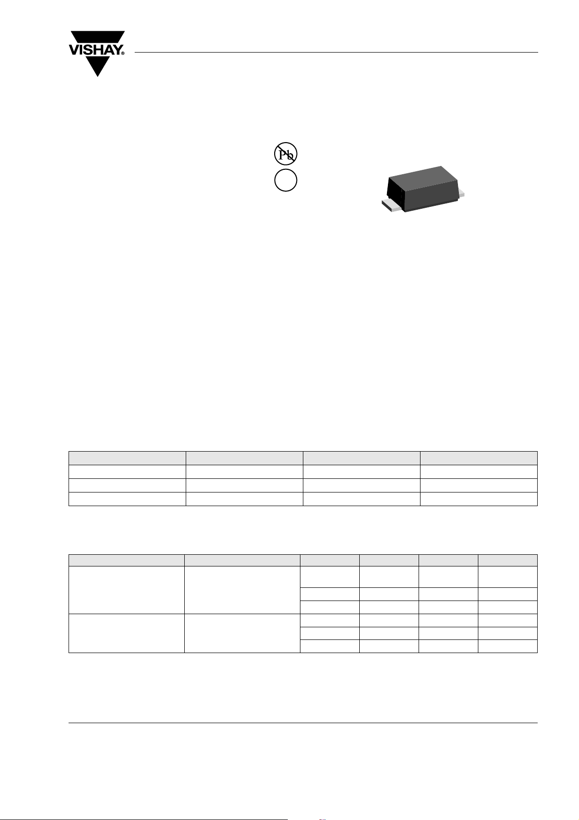
Mechanical Data
Case: JEDEC DO-219AB (SMF) Plastic case
Polarity: Color band denotes cathode end
Weight: approx. 15 mg
Packaging codes-options:
G18 / 10 k per 13" reel (8 mm tape), 50 k/box
G08 / 3 k per 7" reel (8 mm tape), 30 k/box
e3
SL02 / 03 / 04
Vishay Semiconductors
17249
Parts Table
Par t Ordering code Marking Remarks
SL02 SL02-GS18 or SL02-GS08 S2 Tape and Reel
SL03 SL03-GS18 or SL03-GS08 S3 Tape and Reel
SL04 SL04-GS18 or SL04-GS08 S4 Tape and Reel
Absolute Maximum Ratings
T
= 25 °C, unless otherwise specified
amb
Parameter Test condition Part Symbol Val ue Unit
Maximum repetitive peak
reverse voltage
Maximum RMS voltage SL02 V
SL02 V
SL03 V
SL04 V
SL03 V
SL04 V
RRM
RRM
RRM
RMS
RMS
RMS
20 V
30 V
40 V
14 V
21 V
28 V
Document Number 85687
Rev. 1.6, 13-Apr-05
www.vishay.com
1
SL02 / 03 / 04
Vishay Semiconductors
Parameter Test condition Part Symbol Valu e Unit
Maximum DC blocking voltage SL02 V
SL03 V
SL04 V
Maximum average forward
rectified current
Peak forward surge current
8.3 ms single half sine-wave
Thermal Characteristics
T
= 25 °C, unless otherwise specified
amb
Parameter Test condition Symbol Value Unit
Thermal resistance junction to
ambient air
Maximum operating junction
temperature
Storage temperature range T
2)
Mounted on epoxy substrate with 3 x 3 mm Cu pads (≥ 40 μm thick)
2)
T
= 109 °C I
tp
R
thJA
T
J
STG
DC
DC
DC
F(AV)
I
FSM
20 V
30 V
40 V
1.1 A
40 A
180 K/W
125 °C
- 55 to 150 °C
Electrical Characteristics
T
= 25 °C, unless otherwise specified
amb
Parameter Test condition Par t Symbol Min Ty p. Max Unit
Instaneous forward voltage at
1)
0.5
Typical instantaneous forward
voltage
Maximum DC reverse current at
rated DC blocking voltage
1)
Pulse test: 300 μs pulse width, 1 % duty cycle
1.1 A SL02 V
T
= 25 °C SL02 I
A
= 100 °C SL02 I
T
A
T
= 25 °C SL03 I
A
T
= 100 °C SL03 I
A
T
= 25 °C SL04 I
A
T
= 100 °C SL04 I
A
SL02 V
SL03 V
SL04 V
SL03 V
SL04 V
F
F
F
F
F
F
R
R
R
R
R
R
0.360 0.385 V
0.395 0.43 V
0.450 0.51 V
0.420 V
0.450 V
0.530 V
250 μA
8.0 mA
130 μA
6.0 mA
20 μA
6.0 mA
www.vishay.com
2
Document Number 85687
Rev. 1.6, 13-Apr-05
SL02 / 03 / 04
Vishay Semiconductors
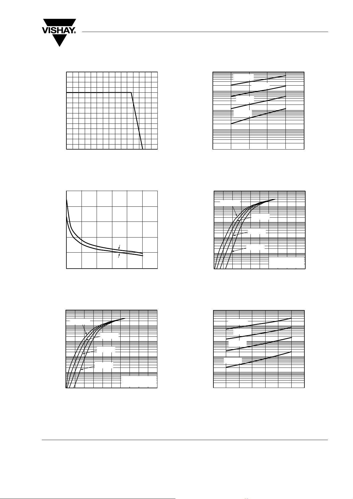
Typical Characteristics (Tamb = 25 °C unless otherwise specified)
17379
17380
1.5
1.0
0.5
Average Forward Current (A)
0
10
0
30
70
50
90
Lead temperature (°C)
Figure 1. Forward Current Derating Curve
250
2
00
150
1
00
SL02
Junction Capacitance (pF)
50
SL04
10
0
2
6
4
Reverse Voltage (V)
Figure 2. Typical Junction Capacitance
10000
TJ=100°C
1000
TJ=75°C
TJ=50°C
110
130
150
17382
100
10
Instantaneous Reverse Current (μA)
1
0
TJ=25°C
10
5
Reverse Voltage (V)
15
20
25
Figure 4. Typical Reverse Current Characteristics - SL02
10
TJ= 100°C
1
TJ=75°C
0.1
TJ=50°C
0.01
TJ=25°C
0.001
Instantaneous Forward Current (A)
8
10
1
2
0.0001
17383
0.2
0.1
0
Instantaneous Forward Voltage (V)
0.3
0.4
Pulse Width = 300μs
1% Duty Cycle
0.6
0.5
0.7
0.8
0.9
1.0
Figure 5. Typical Instantaneous Forward Characteristics - SL03
10
TJ= 100°C
1
TJ=75°C
0.1
TJ=50°C
0
.01
TJ=25°C
0.001
0.0001
17381
Instantaneous Forward Current (A)
0
0
.1
0
0
0
.2
.4
.3
Instantaneous Forward Voltage (V)
Pulse Width = 300μs
1% Duty Cycle
0
0
.6
.5
0
.7
.9
.8
1.0
0
0
Figure 3. Typical Instantaneous Forward Characterisics - SL02
Document Number 85687
Rev. 1.6, 13-Apr-05
10000
1000
TJ= 100°C
TJ=75°C
17384
100
10
1
Instantaneous Reverse Current (μA)
0.1
TJ=50°C
TJ=25°C
5
0
15
10
25
20
35
30
Reverse Voltage (V)
Figure 6. Typical Reverse Current Characteristics - SL03
www.vishay.com
3

SL02 / 03 / 04
Vishay Semiconductors
Package Dimensions in mm (Inches)
5
0.85 (0.033)
0.35 (0.014)
3.9 (0.152)
3.5 (0.137)
Detail
Z
enlarged
ISO Method E
0.10 max
5
0.99 (0.039)
0.97 (0.038)
1.9 (0.074)
1.7 (0.066)
0.16 (0.006)
Z
Cathode Band
Top View
1.2 (0.047)
0.8 (0.031)
2.9 (0.113)
2.7 (0.105)
Mounting Pad Layout
1.6 (0.062) 1.3 (0.051)
www.vishay.com
4
1.4 (0.055)
17247
Document Number 85687
Rev. 1.6, 13-Apr-05

Blistertape for SMF
SL02 / 03 / 04
Vishay Semiconductors
PS
18513
Document Number 85687
Rev. 1.6, 13-Apr-05
www.vishay.com
5

SL02 / 03 / 04
Vishay Semiconductors
Ozone Depleting Substances Policy Statement
It is the policy of Vishay Semiconductor GmbH to
1. Meet all present and future national and international statutory requirements.
2. Regularly and continuously improve the performance of our products, processes, distribution and operating
systems with respect to their impact on the health and safety of our employees and the public, as well as
their impact on the environment.
It is particular concern to control or eliminate releases of those substances into the atmosphere which are
known as ozone depleting substances (ODSs).
The Montreal Protocol (1987) and its London Amendments (1990) intend to severely restrict the use of ODSs
and forbid their use within the next ten years. Various national and international initiatives are pressing for an
earlier ban on these substances.
Vishay Semiconductor GmbH has been able to use its policy of continuous improvements to eliminate the use
of ODSs listed in the following documents.
1. Annex A, B and list of transitional substances of the Montreal Protocol and the London Amendments
respectively
2. Class I and II ozone depleting substances in the Clean Air Act Amendments of 1990 by the Environmental
Protection Agency (EPA) in the USA
3. Council Decision 88/540/EEC and 91/690/EEC Annex A, B and C (transitional substances) respectively.
Vishay Semiconductor GmbH can certify that our semiconductors are not manufactured with ozone depleting
substances and do not contain such substances.
We reserve the right to make changes to improve technical design
and may do so without further notice.
Parameters can vary in different applications. All operating parameters must be validated for each
customer application by the customer. Should the buyer use Vishay Semiconductors products for any
unintended or unauthorized application, the buyer shall indemnify Vishay Semiconductors against all
claims, costs, damages, and expenses, arising out of, directly or indirectly, any claim of personal
damage, injury or death associated with such unintended or unauthorized use.
Vishay Semiconductor GmbH, P.O.B. 3535, D-74025 Heilbronn, Germany
www.vishay.com
6
Document Number 85687
Rev. 1.6, 13-Apr-05

Legal Disclaimer Notice
Vishay
Notice
Specifications of the products displayed herein are subject to change without notice. Vishay Intertechnology, Inc.,
or anyone on its behalf, assumes no responsibility or liability for any errors or inaccuracies.
Information contained herein is intended to provide a product description only. No license, express or implied, by
estoppel or otherwise, to any intellectual property rights is granted by this document. Except as provided in Vishay's
terms and conditions of sale for such products, Vishay assumes no liability whatsoever, and disclaims any express
or implied warranty, relating to sale and/or use of Vishay products including liability or warranties relating to fitness
for a particular purpose, merchantability, or infringement of any patent, copyright, or other intellectual property right.
The products shown herein are not designed for use in medical, life-saving, or life-sustaining applications.
Customers using or selling these products for use in such applications do so at their own risk and agree to fully
indemnify Vishay for any damages resulting from such improper use or sale.
Document Number: 91000 www.vishay.com
Revision: 08-Apr-05 1
 Loading...