

N-Channel 30 V (D-S) MOSFET
Ordering Information: SiS472DN-T1-GE3 (Lead (Pb)-free and Halogen-free)
1
2
3
4
5
6
7
8
S
S
S
G
D
D
D
D
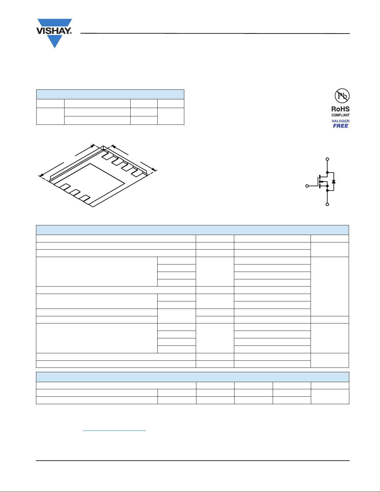
3.30 mm 3.30 mm
PowerPAK
®
1212-8
Bottom View
SiS472DN
Vishay Siliconix
PRODUCT SUMMARY
VDS (V) R
30
0.0089 at V
0.0124 at V
()I
DS(on)
= 10 V 20
GS
= 4.5 V 20
GS
D
(A)
a, g
Qg (Typ.)
9.8 nC
FEATURES
• Halogen-free According to IEC 61249-2-21
Definition
• TrenchFET
• Optimized for High-Side Synchronous
®
Power MOSFET
Rectifier Operation
• 100 % R
Tested
g
• 100 % UIS Tested
• Compliant to RoHS Directive 2002/95/EC
APPLICATIONS
D
• Notebook CPU Core
- High-Side Sw
itch
G
S
N-Channel MOSFET
ABSOLUTE MAXIMUM RATINGS (TA = 25 °C, unless otherwise noted)
Parameter Symbol Limit Unit
Drain-Source Voltage V
Gate-Source Voltage V
T
= 25 °C
C
= 70 °C
T
Continuous Drain Current (T
= 150 °C)
J
C
TA = 25 °C
TA = 70 °C
Pulsed Drain Current I
T
= 25 °C
Continuous Source-Drain Diode Current
Single Pulse Avalanche Current
Avalanche Energy E
Maximum Power Dissipation
C
TA = 25 °C
L = 0.1 mH
T
= 25 °C
C
T
= 70 °C 18
C
T
= 25 °C
A
I
P
TA = 70 °C
Operating Junction and Storage Temperature Range TJ, T
Soldering Recommendations (Peak Temperature)
d, e
DS
GS
I
D
DM
I
AS
AS
S
D
stg
30
± 20
g
20
g
20
b, c
15
b, c
12
50
g
20
b, c
3.2
21
22 mJ
28
b, c
3.5
b, c
2.2
- 55 to 150
260
V
A
W
°C
THERMAL RESISTANCE RATINGS
Parameter Symbol Typical Maximum Unit
Maximum Junction-to-Ambient
Maximum Junction-to-Case (Drain) Steady State R
Notes:
a. Base on T
b. Surface mounted on 1" x 1" FR4 board.
c. t = 10 s.
d. See solder profile (www.vishay.com/ppg?73257
(not plated) as a result of the singulation process in manufacturing. A solder fillet at the exposed copper tip cannot be guaranteed and is not
required to ensure adequate bottom side solder interconnection.
e. Rework conditions: manual soldering with a soldering iron is not recommended for leadless components.
f. Maximum under steady state conditions is 81 °C/W.
g. Package limited.
Document Number: 67307
S10-2882-Rev. A, 20-Dec-10
= 25 °C.
C
b, f
t 10 s R
thJA
thJC
29 36
3.6 4.5
°C/W
). The PowerPAK® 1212 is a leadless package. The end of the lead terminal is exposed copper
www.vishay.com
1
SiS472DN
Vishay Siliconix
SPECIFICATIONS (TJ = 25 °C, unless otherwise noted)
Parameter Symbol Test Conditions Min. Typ. Max. Unit
Static
Drain-Source Breakdown Voltage V
Temperature Coefficient VDS/T
V
DS
V
Temperature Coefficient V
GS(th)
Gate-Source Threshold Voltage V
Gate-Source Leakage I
Zero Gate Voltage Drain Current I
On-State Drain Current
Drain-Source On-State Resistance
Forward Transconductance
Dynamic
b
a
a
a
Input Capacitance C
Reverse Transfer Capacitance C
Total Gate Charge Q
Gate-Source Charge Q
Gate-Drain Charge Q
Gate Resistance R
Tur n -O n D el a y T im e t
Rise Time t
Turn-Off Delay Time t
Fall Time t
Tur n -O n D el a y T im e t
Rise Time t
Turn-Off Delay Time t
Fall Time t
DS
J
GS(th)/TJ
GS(th)
GSS
DSS
I
V
D(on)
R
DS(on)
g
fs
iss
oss
120
rss
g
gs
3.7
gd
g
d(on)
r
19 29
d(off)
f
d(on)
r
18 27
d(off)
f
Drain-Source Body Diode Characteristics
Continuous Source-Drain Diode Current I
Pulse Diode Forward Current
a
Body Diode Voltage V
Body Diode Reverse Recovery Time t
Body Diode Reverse Recovery Charge Q
Reverse Recovery Fall Time t
Reverse Recovery Rise Time t
S
I
SM
SD
rr
rr
a
b
Notes:
a. Pulse test; pulse width 300 µs, duty cycle 2 %.
b. Guaranteed by design, not subject to production testing.
Stresses beyond those listed under “Absolute Maximum Ratings” may cause permanent damage to the device. These are stress ratings only, and functional operation
of the device at these or any other conditions beyond those indicated in the operational sections of the specifications is not implied. Exposure to absolute maximum
rating conditions for extended periods may affect device reliability.
VGS = 0 V, ID = 250 µA 30 V
ID = 250 µA
V
= VGS, ID = 250 µA 1.2 2.5 V
DS
28
- 5.5
VDS = 0 V, VGS = ± 20 V ± 100 nA
V
V
DS
= 30 V, V
DS
= 30 V, V
GS
5 V, V
DS
V
= 10 V, ID = 15 A 0.0074 0.0089
GS
V
= 4.5 V, ID = 13 A 0.0103 0.0124
GS
= 0 V 1
GS
= 0 V, TJ = 55 °C 10
= 10 V 20 A
GS
VDS = 15 V, ID = 13 A 49 S
997
VDS = 15 V, V
VDS = 15 V, V
= 0 V, f = 1 MHz
GS
= 10 V, ID = 15 A 19.5 30
GS
195
9.8 15
V
= 15 V, V
DS
= 4.5 V, ID = 15 A
GS
3.7
f = 1 MHz 0.2 1.2 2.4
19 29
V
I
10 A, V
D
= 15 V, RL = 1.5
DD
= 4.5 V, Rg = 1
GEN
19 29
13 20
918
V
I
10 A, V
D
= 15 V, RL = 1.5
DD
= 10 V, Rg = 1
GEN
918
815
TC = 25 °C 20
IS = 10 A 0.85 1.2 V
14 28 ns
IF = 10 A, dI/dt = 100 A/µs, TJ = 25 °C
510nC
7
7
50
mV/°C
µA
pFOutput Capacitance C
nC
ns
A
ns
www.vishay.com
2
Document Number: 67307
S10-2882-Rev. A, 20-Dec-10
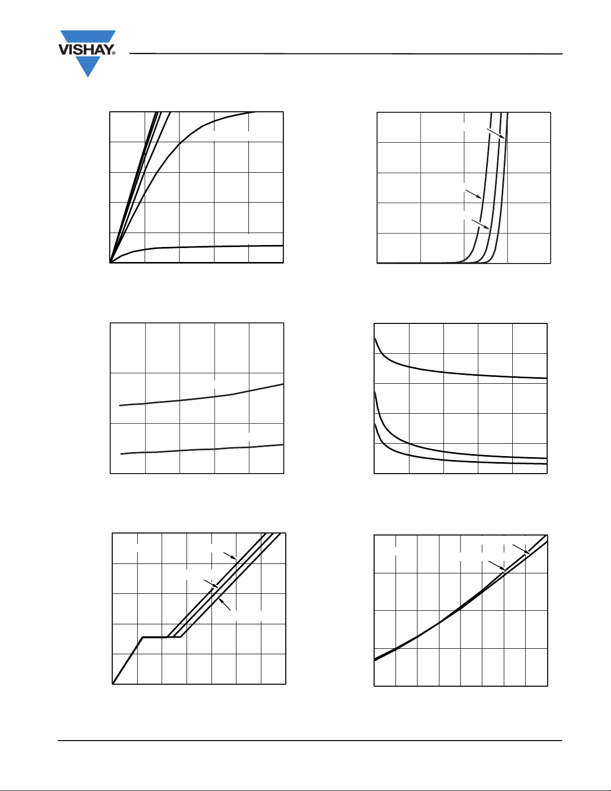
TYPICAL CHARACTERISTICS (25 °C, unless otherwise noted)
0
10
20
30
40
50
0.0 0.3 0.6 0.9 1.2 1.5
VDS- Drain-to-Source Voltage (V)
I
D
- Drain Current (A)
VGS=10V thru 5 V
VGS=4V
0.006
0.009
0.012
0.015
0 1020304050
R
DS(on)
- On-Resistance (Ω)
I
D
- Drain Current (A)
VGS=4.5V
VGS=10V
0
1
2
3
4
5
01234
V
GS
- Gate-to-Source Voltage (V)
I
D
- Drain Current (A)
TC= 25 °C
TC= 125 °C
TC= - 55 °C
0.5
0.8
1.1
1.4
1.7
- 50 - 25 0 25 50 75 100 125 150
TJ- Junction Temperature (°C)
(Normalized)
- On-Resistance
R
DS(on)
VGS=4.5V
ID= 15 A
VGS=10V
SiS472DN
Vishay Siliconix
Output Characteristics
On-Resistance vs. Drain Current and Gate Voltage
10
ID= 15 A
8
VDS= 8 V
VDS= 15 V
Transfer Characteristics
1500
C
1200
900
600
C - Capacitance (pF)
300
iss
C
oss
C
rss
0
0 6 12 18 24 30
VDS- Drain-to-Source Voltage (V)
Capacitance
6
4
- Gate-to-Source Voltage (V)
GS
2
V
0
0369121518 21
Qg- Total Gate Charge (nC)
Gate Charge
Document Number: 67307
S10-2882-Rev. A, 20-Dec-10
VDS= 24 V
On-Resistance vs. Junction Temperature
www.vishay.com
3
SiS472DN
1.0
1.3
1.6
1.9
2.2
2.5
- 50 - 25 0 25 50 75 100 125 150
ID=250µA
V (V)
GS(th)
TJ- Temperature (°C)
Vishay Siliconix
TYPICAL CHARACTERISTICS (25 °C, unless otherwise noted)
100
10
1
- Source Current (A)
S
I
0.1
0.0 0.3 0.6 0.9 1.2
TJ= 150 °C
V
- Source-to-Drain Voltage (V)
SD
TJ= 25 °C
Source-Drain Diode Forward Voltage
0.030
0.020
TJ= 125 °C
- On-Resistance (Ω)
0.010
DS(on)
R
0.000
2345678 910
VGS- Gate-to-Source Voltage (V)
TJ= 25 °C
On-Resistance vs. Gate-to-Source Voltage
120
96
72
Power (W)
48
24
0
0.1
Time (s)
Threshold Voltage
100
Limited by R
10
1
- Drain Current (A)
D
I
0.1
TC= 25 °C
Single Pulse
0.01
0.1 1 10 100
* V
> minimum VGSat which R
GS
*
DS(on)
BVDSS Limited
VDS- Drain-to-Source Voltage (V)
DS(on)
Single Pulse Power, Junction-to-Ambient
100 μs
1 ms
10 ms
100 ms
1 s
10 s
DC
is specied
011100.00.01
Safe Operating Area, Junction-to-Ambient
www.vishay.com
4
Document Number: 67307
S10-2882-Rev. A, 20-Dec-10
 Loading...