Vishay SiP32431DNP3, SiP32431DR3 Schematic [ru]
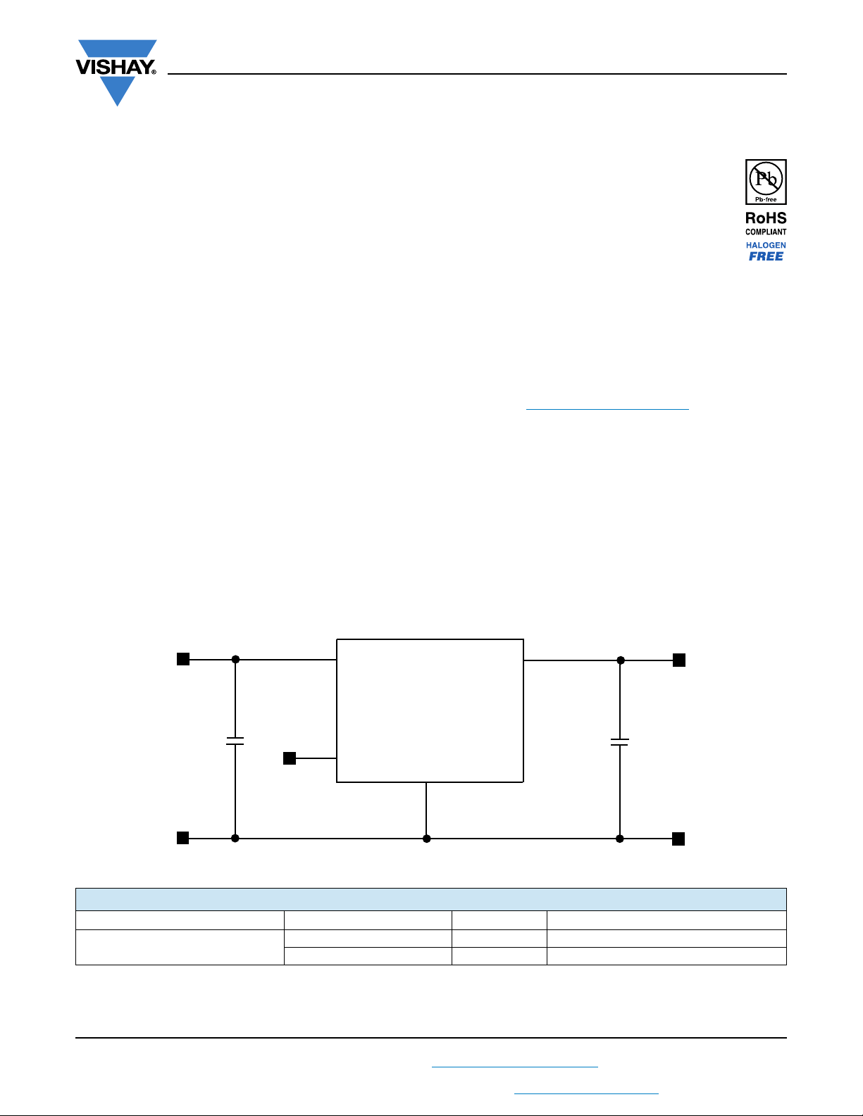
SiP32431
SiP32431
IN
V
OUT
OUT
V
IN
GND
GND
GND
ON/OFF
ON/OFF
C
1 µF
IN
C
0.1 µF
OUT
www.vishay.com
Vishay Siliconix
1 A Slew Rate Controlled Load Switch with Reverse Blocking
DESCRIPTION
The SiP32431 is a slew rate controlled high side switch with
reverse blocking capability. The switch is of a low ON
resistance p-channel MOSFET that supports continuous
current up to 1 A.
The SiP32431 operates with an input voltage from 1.5 V to
5.5 V.
The SiP32431 features low input logic level to interface with
low control voltage from microprocessors. This device has a
very low operating current, typically 50 pA.
The SiP32431 is available in lead (Pb)-free package options
including 6 pin SC70-6, and 4 pin TDFN4 1.2 mm x 1.6 mm
DFN4 packages. The operation temperature range is
specified from -40 °C to +85 °C.
The SiP32431 compact package options, operation voltage
range, and low operating current make it a good fit for
battery power applications.
FEATURES
• 1.5 V to 5.5 V input voltage range
• Very low R
, typically 105 mΩ at 5 V and
DS(on)
135 mΩ at 3 V for TDFN4 1.2 mm x 1.6 mm
package
• Typical 147 mΩ at 5 V and 178 mΩ at 3 V for
SC70-6 package
Available
• Slew rate controlled turn-on time: 100 μs
• Low quiescent current < 1 μA
• Low shutdown current < 1 μA
• Reverse blocking capability
• SC70-6 and TDFN4 1.2 mm x 1.6 mm packages
• Material categorization: for definitions of compliance
please see www.vishay.com/doc?99912
APPLICATIONS
• Cellular telephones
• Digital still cameras
• Personal digital assistants (PDA)
• Hot swap supplies
• Notebook computers
• Personal communication devices
• Portable Instruments
TYPICAL APPLICATION CIRCUIT
Fig. 1 - SiP32431 Typical Application Circuit
ORDERING INFORMATION
TEMPERATURE RANGE PACKAGE MARKING PART NUMBER
-40 °C to 85 °C
Notes
•x = lot code
• -GE3 denotes halogen-free and RoHS-compliant
• Please use the SiP32431DR3-T1GE3 to replace SiP32431DR3-T1-E3
S15-1821-Rev. C, 10-Aug-15
THIS DOCUMENT IS SUBJECT TO CHANGE WITHOUT NOTICE. THE PRODUCTS DESCRIBED HEREIN AND THIS DOCUMENT
TDFN4 1.2 mm x 1.6 mm Dx SiP32431DNP3-T1GE4
For technical questions, contact: powerictechsupport@vishay.com
ARE SUBJECT TO SPECIFIC DISCLAIMERS, SET FORTH AT www.vishay.com/doc?91000
SC70-6 MAxx SiP32431DR3-T1GE3
1
Document Number: 66597
SiP32431
www.vishay.com
ABSOLUTE MAXIMUM RATINGS
PARAMETER LIMIT UNIT
Supply Input Voltage (V
Output Voltage (V
Maximum Continuous Switch Current (I
Maximum Pulsed Current (I
(pulsed at 1 ms, 10 % duty cycle)
ESD Rating (HBM) 4000 V
Junction Temperature (T
Thermal Resistance (θ
Power Dissipation (P
Notes
a. Device mounted with all leads and power pad soldered or welded to PC board.
b. Derate 4.5 mW/°C above T
c. Derate 5.9 mW/°C above T
Stresses beyond those listed under "Absolute Maximum Ratings" may cause permanent damage to the device. These are stress ratings only, and functional operation
of the device at these or any other conditions beyond those indicated in the operational sections of the specifications is not implied. Exposure to absolute maximum
rating/conditions for extended periods may affect device reliability.
) -0.3 to 6
IN
) -0.3 to 6
ON/OFF
) -0.3 to VIN +0.3
OUT
)
max.
) VIN
DM
) -40 to 125 °C
J
a
)
JA
a
)
D
= 70 °C.
A
= 70 °C, see PCB layout.
A
SC70-6 package 1.2
TDFN4 1.2 mm x 1.6 mm 1.4
V
≥ 2.5 V 3
IN
V
< 2.5 V 1.6
IN
6 pin SC70-6
4 pin TDFN4 1.2 mm x 1.6 mm
6 pin SC70- 6
4 pin TDFN4 1.2 mm x 1.6 mm
b
c
b
c
220
170
250
324
Vishay Siliconix
VEnable Input Voltage (V
A
°C/W
mW
RECOMMENDED OPERATING RANGE
PARAMETER LIMIT UNIT
Input Voltage Range (V
Operating Temperature Range -40 to 85 °C
) 1.5 to 5.5 V
IN
S15-1821-Rev. C, 10-Aug-15
2
Document Number: 66597
For technical questions, contact: powerictechsupport@vishay.com
THIS DOCUMENT IS SUBJECT TO CHANGE WITHOUT NOTICE. THE PRODUCTS DESCRIBED HEREIN AND THIS DOCUMENT
ARE SUBJECT TO SPECIFIC DISCLAIMERS, SET FORTH AT www.vishay.com/doc?91000
www.vishay.com
OUT
1
GND
2
ON/OFF
3
N/C
6
GND
5
IN
4
Top View
SPECIFICATIONS
PARAMETER SYMBOL
Operating Voltage
Quiescent Current I
Off Supply Current I
Off Switch Current I
Reverse Blocking Current I
c
V
IN
Q
Q(off)
SD(off)
RB
V
On-Resistance R
DS(on)
V
V
On-Resistance Temp.-Coefficient TD
RDS
VIN = 5, TA = -40 °C to 85 °C
(Typical values are at T
= 25 °C)
A
On/off = active - 0.00005 1
On/off = inactive, out = open - - 1
On/off = inactive, out = 0 - - 1
V
= 5.5 V, VIN = 0, V
OUT
VIN = 5 V, IL = 500 mA, TA = 25 °C
= 4.2 V, IL = 500 mA, TA = 25 °C
IN
= 3 V, IL = 500 mA, TA = 25 °C
V
IN
= 1.8 V, IL = 500 mA, TA = 25 °C
IN
= 1.5 V, IL = 500 mA, TA = 25 °C
IN
= inactive - 0.13 1
on/off
SC70-6 - 147
TDFN4 - 105
SC70-6 - 155
TDFN4 - 110
SC70-6 - 178
TDFN4 - 135
SC70-6 - 275
TDFN4 - 230
SC70-6 - 395
TDFN4 - 350
VIN ≥ 1.5 V to < 1.8 V - - 0.3
TEST CONDITIONS UNLESS SPECIFIED
On/Off Input Low Voltage
c
V
IL
V
≥ 1.8 V to < 2.7 V - - 0.4
IN
V
≥ 2.7 V to ≤ 5.5 V - - 0.6
IN
VIN ≥ 1.5 V to < 2.7 V 1.3 - -
V
On/Off Input Low Voltage c V
On/Off Input Leakage I
Output Turn-On Delay Time t
Output Turn-Off Delay Time t
SINK
d(on)
(on)
d(off)
IH
VIN = 5 V, R
≥ 2.7 V to < 4.2 V 1.5 - -
IN
V
≥ 4.2 V to ≤ 5.5 V 1.8 - -
IN
V
= 5.5 V - - 1 μA
On/Off
= 10 Ω, TA = 25 °C
load
Notes
a. The algebriac convention whereby the most negative value is a minimum and the most positive a maximum.
b. Typical values are for DESIGN AID ONLY, not guaranteed nor subject to production testing
c. For V
outside this range consult typical on/off threshold curve.
IN
-40 °C TO 85 °C
a
MIN.
TYP. bMAX.
1.5 - 5.5 V
- 2800 - ppm/°C
-2040
- 140 180
-410
SiP32431
Vishay Siliconix
LIMITS
a
230
250
290
480
520
UNIT
μA
mΩ
V
μsOutput Turn-On Rise Time t
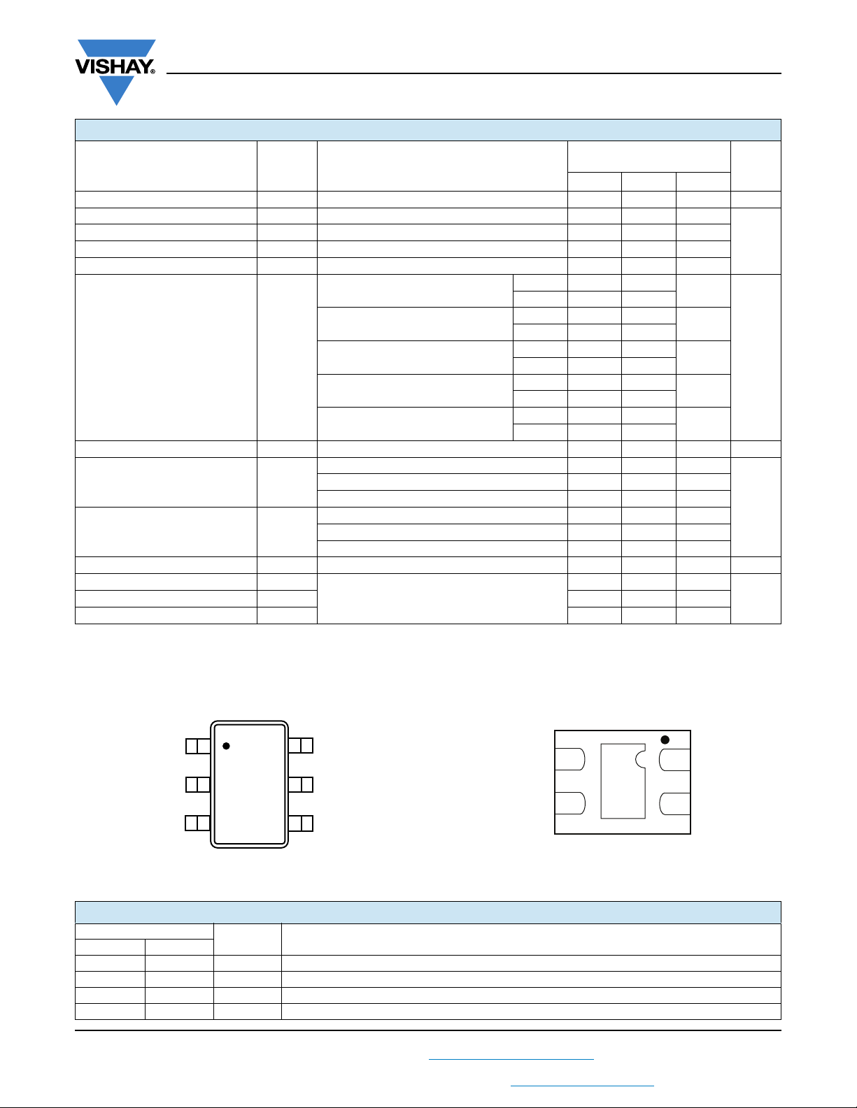
PIN CONFIGURATION
Fig. 2 - SC70-6 Package Fig. 3 - TDFN4 1.2 mm x 1.6 mm Package
PIN DESCRIPTION
PIN NUMBER
SC70-6 TDFN4
4 3 IN This pin is the p-channel MOSFET source connection. Bypass to ground through a 1 μF capacitor
2, 5 2 GND Ground connection
3 4 ON/OFF Enable input
1 1 OUT This pin is the p-channel MOSFET drain connection. Bypass to ground through a 0.1 μF capacitor
S15-1821-Rev. C, 10-Aug-15
THIS DOCUMENT IS SUBJECT TO CHANGE WITHOUT NOTICE. THE PRODUCTS DESCRIBED HEREIN AND THIS DOCUMENT
ON/OFF
4
GND
IN
3
Bottom View
NAME FUNCTION
3
For technical questions, contact: powerictechsupport@vishay.com
ARE SUBJECT TO SPECIFIC DISCLAIMERS, SET FORTH AT www.vishay.com/doc?91000
OUT
1
2
GND
Document Number: 66597
www.vishay.com
0
1.5 2.0 2.5 3.5 4.5 5.53.0 4.0 5.0
0.04
0.02
0.06
0.08
0.10
0.12
VIN (V)
I
Q
- Quiescent Current (nA)
0
1.5 2.0 2.5 3.5 5.0 6.03.0 4.0 5.54.5
150
50
250
200
100
300
350
VIN (V)
I
SD(OFF)
- Off Switch Current (nA)
0
- 40 - 20 0 40 10020 60 80
150
50
250
200
100
300
Temperature (°C)
I
SD(OFF)
- Off Switch Current (nA)
VIN = 5 V
1.0 1.5 2.0 3.0 4.0 5.52.5 3.5 4.5 5.0
V
IN
(V)
R
DS
- On-Resistance (mΩ)
50
100
150
200
250
300
350
400
450
500
550
for SC70-6 package
IL= 1.2 A
IL= 500 mA
IL= 100 mA
TYPICAL CHARACTERISTICS (internally regulated, 25 °C, unless otherwise noted)
SiP32431
Vishay Siliconix
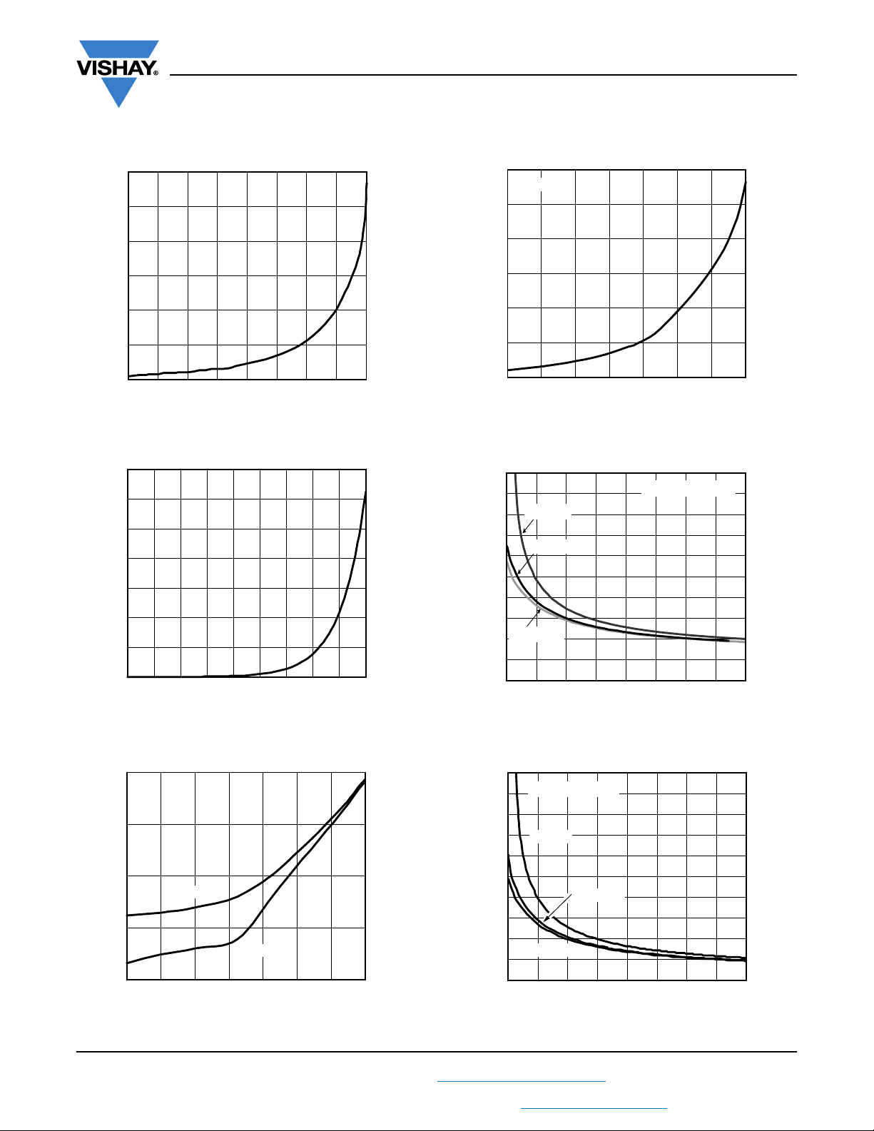
Fig. 4 - Quiescent Current vs. Input Voltage
Fig. 5 - Off Switch Current vs. Input Voltage
10
1
0.1
VIN = 5 V
- Quiescent Current (nA)
Q
0.01
I
0.001
- 40 - 20 0 40 80 10020 60
Fig. 6 - Quiescent Current vs. Temperature
S15-1821-Rev. C, 10-Aug-15
THIS DOCUMENT IS SUBJECT TO CHANGE WITHOUT NOTICE. THE PRODUCTS DESCRIBED HEREIN AND THIS DOCUMENT
Fig. 7 - Off Switch Current vs. Temperature
VIN = 3 V
Temperature (°C)
Fig. 8 - R
550
500
450
400
350
300
250
- On-Resistance (mΩ)
200
DS
R
150
100
for TDFN4 package
IL = 1.2 A
IL = 100 mA
50
1.5 2.0 2.5 3.5 5.53.0 4.0 4.5 5.0
Fig. 9 - R
vs. VIN for SC70-6 Package
DS(on)
IL = 500 mA
VIN (V)
vs. Input Voltage
DS(on)
4
For technical questions, contact: powerictechsupport@vishay.com
ARE SUBJECT TO SPECIFIC DISCLAIMERS, SET FORTH AT www.vishay.com/doc?91000
Document Number: 66597
www.vishay.com
V
OUT
(V)
I
RB
- Reverse Blocking Current (nA)
0.01
0.1
1
10
100
1000
0 0.5 1 1.5 2 2.5 3 3.5 4 4.5 5 5.5
VIN = 0 V
- 40 - 20 0 40 80 10020 60
Temperature (°C)
R
DS
- On-Resistance (mΩ)
120
130
140
150
160
170
180
190
200
210
220
VIN = 5 V
VIN = 3 V
I
LOAD
= 500 mA
for SC70-6 package
60
- 40 - 20 0 40 10020 60 80
140
80
100
180
120
160
Temperature (°C)
R
DS
- On-Resistance (mΩ)
VIN = 5 V
VIN = 3 V
I
LOAD
= 500 mA
for TDFN4 package
0.4
1.5 2.0 2.5 3.5 6.03.0 4.0 5.04.5 5.5
1.2
0.6
0.8
1.6
1.0
1.4
VIN (V)
On/Off Threshold Voltage (V)
V
IH
V
IL
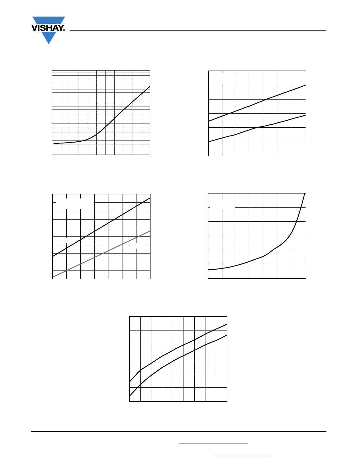
TYPICAL CHARACTERISTICS (internally regulated, 25 °C, unless otherwise noted)
SiP32431
Vishay Siliconix
Fig. 10 - Reverse Blocking Current vs. V
Fig. 11 - R
vs. Temperature
DS(on)
OUT
Fig. 12 - R
600
V
= 5.5 V
OUT
500
= 0 V
V
IN
400
300
200
- Reverse Blocking Current (nA)
100
RB
I
0
- 40 - 20 0 40 10020 60 80
vs. Temperature
DS(on)
Temperature (°C)
Fig. 13 - Reverse Blocking Current vs. Temperature
S15-1821-Rev. C, 10-Aug-15
THIS DOCUMENT IS SUBJECT TO CHANGE WITHOUT NOTICE. THE PRODUCTS DESCRIBED HEREIN AND THIS DOCUMENT
ARE SUBJECT TO SPECIFIC DISCLAIMERS, SET FORTH AT www.vishay.com/doc?91000
Fig. 14 - On/Off Threshold vs. Input Voltage
5
For technical questions, contact: powerictechsupport@vishay.com
Document Number: 66597
