Vishay SiHP18N50C Data Sheet

N-Channel MOSFET
G
D
S
TO-220AB
G
D
S
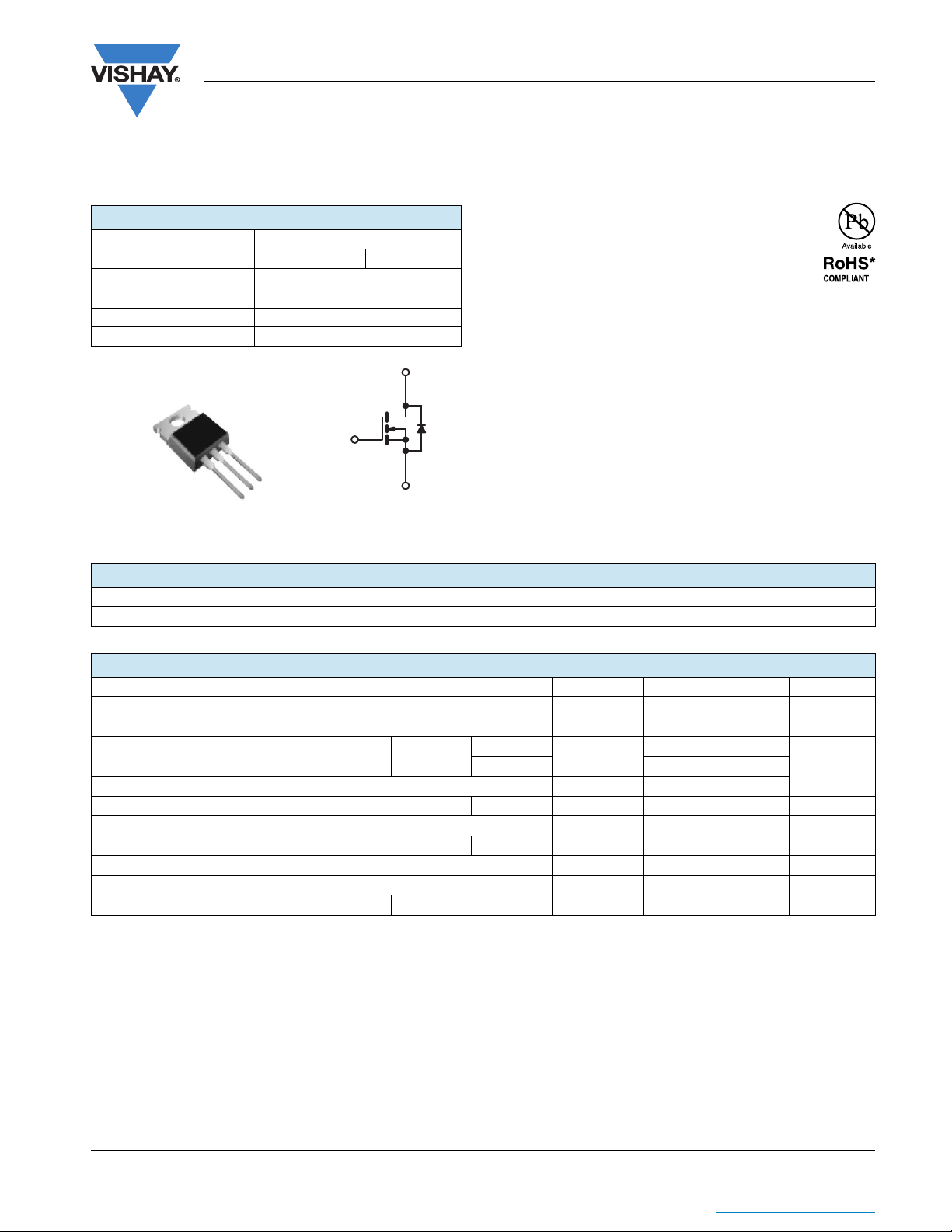
Power MOSFET
SiHP18N50C
Vishay Siliconix
PRODUCT SUMMARY
VDS (V) at TJ max. 560
R
()V
DS(on)
Q
(Max.) (nC) 76
g
Q
(nC) 21
gs
Q
(nC) 29
gd
Configuration Single
= 10 V 0.225
GS
FEATURES
• Low Figure-of-Merit Ron x Q
• 100 % Avalanche Tested
• High Peak Current Capability
• dV/dt Ruggedness
• Improved t
• Improved Gate Charge
rr/Qrr
g
• High Power Dissipations Capability
• Compliant to RoHS Directive 2002/95/EC
ORDERING INFORMATION
Package TO-220AB
Lead (Pb)-free SiHP18N50C-E3
ABSOLUTE MAXIMUM RATINGS (TC = 25 °C, unless otherwise noted)
PARAMETER SYMBOL LIMIT UNIT
Drain-Source Voltage V
Gate-Source Voltage V
T
= 25 °C
Continuous Drain Current (T
Pulsed Drain Current
b
= 150 °C)
J
a
VGS at 10 V
C
= 100 °C 11
C
DS
± 30
GS
I
D
IDM 72
Linear Derating Factor TO-220AB 1.8 W/°C
Single Pulse Avalanche Energy
Maximum Power Dissipation TO-220AB P
Peak Diode Recovery dV/dt
Operating Junction and Storage Temperature Range T
Soldering Recommendations (Peak Temperature)
c
d
d
for 10 s 300
E
AS
D
dV/dt 5 V/ns
, T
J
stg
Notes
a. Drain current limited by maximum junction temperature.
b. Repetitive rating; pulse width limited by maximum junction temperature.
c. V
= 50 V, starting TJ = 25 °C, L = 2.5 mH, Rg = 25 , IAS = 17 A.
DD
d. I
18 A, dI/dt 380 A/μs, VDD VDS, TJ 150 °C.
SD
e. 1.6 mm from case.
500
18
361 mJ
223 W
- 55 to + 150
V
AT
°C
* Pb containing terminations are not RoHS compliant, exemptions may apply
Document Number: 91374 www.vishay.com
S11-0520-Rev. D, 21-Mar-11 1
THE PRODUCT DESCRIBED HEREIN AND THIS DATASHEET ARE SUBJECT TO SPECIFIC DISCLAIMERS, SET FORTH AT
This datasheet is subject to change without notice.
www.vishay.com/doc?91000

SiHP18N50C
Vishay Siliconix
THERMAL RESISTANCE RATINGS
PARAMETER SYMBOL TYP. MAX. UNIT
Maximum Junction-to-Ambient TO-220 R
Maximum Junction-to-Case (Drain) TO-220 R
thJA
thJC
SPECIFICATIONS (TJ = 25 °C, unless otherwise noted)
PARAMETER SYMBOL TEST CONDITIONS MIN. TYP. MAX. UNIT
Static
Drain-Source Breakdown Voltage V
V
Temperature Coefficient VDS/TJ Reference to 25 °C, ID = 1 mA - 0.6 - V/°C
DS
Gate-Source Threshold Voltage (N) V
Gate-Source Leakage I
Zero Gate Voltage Drain Current I
Drain-Source On-State Resistance R
Forward Transconductance
a
DS
GS(th)
V
GSS
DSS
VGS = 10 V ID = 10 A - 0.225 0.270
DS(on)
g
fs
Dynamic
Input Capacitance C
Reverse Transfer Capacitance C
Internal Gate Resistance R
Total Gate Charge Q
iss
- 300 360
oss
-2632
rss
f = 1.0 MHz, open drain - 1.1 -
g
g
V
Gate-Drain Charge Q
Turn-On Delay Time t
Rise Time t
Turn-Off Delay Time t
Fall Time t
-29-
gd
d(on)
r
-32-
d(off)
-44-
f
Drain-Source Body Diode Characteristics
Continuous Source-Drain Diode Current I
Pulsed Diode Forward Current I
Body Diode Voltage V
Body Diode Reverse Recovery Time t
Body Diode Reverse Recovery Charge Q
Reverse Recovery Current I
S
SM
SD
rr
rr
RRM
MOSFET symbol
showing the
integral reverse
p - n junction diode
Note
a. Repetitive rating; pulse width limited by maximum junction temperature.
VGS = 0 V, ID = 250 μA 500 - - V
VDS = VGS, ID = 250 μA 3.0 - 5.0 V
= ± 30 V - - ± 100 nA
GS
VDS = 500 V, VGS = 0 V - - 25
V
= 400 V, VGS = 0 V, TJ = 125 °C - - 250
DS
VDS = 50 V, ID = 10 A - 6.4 - S
VGS = 0 V,
= 25 V,
V
DS
f = 1.0 MHz
= 10 V ID = 18 A, VDS = 400 V
GS
V
= 250 V, ID = 18 A
DD
R
= 7.5 , V
g
TJ = 25 °C, IS = 18 A, VGS = 0 V - - 1.5 V
TJ = 25 °C, IF = IS,
dI/dt = 100 A/μs, V
-62
-0.56
- 2451 2942
-6576
-80-
-27-
= 10 V
GS
D
G
S
--18
--72
- 503 - ns
= 35 V
R
-6.7-μC
-30-A
°C/W
μA
pFOutput Capacitance C
nC Gate-Source Charge Qgs -21-
ns
A
The information shown here is a preliminary product proposal, not a commercial product datasheet. Vishay Siliconix is not committed to produce this or any similar
product. This information should not be used for design purposes, nor construed as an offer to furnish or sell such products.
www.vishay.com Document Number: 91374
2 S11-0520-Rev. D, 21-Mar-11
This datasheet is subject to change without notice.
THE PRODUCT DESCRIBED HEREIN AND THIS DATASHEET ARE SUBJECT TO SPECIFIC DISCLAIMERS, SET FORTH AT
www.vishay.com/doc?91000

VDS, Drain-to-Source Voltage (V)
I
D
, Drain Current (A)
0
10
20
30
40
50
60
70
0612 18
24
30
7.0 V
Bottom
To p
V
GS
15 V
14 V
13 V
12 V
11 V
10 V
9.0 V
8.0 V
7.0 V
6.0 V
5.0 V
TJ = 25 °C
0
I
D
, Drain Current (A)
V
GS
,
Gate-to-Source Voltage (V)
0.01
0.1
1
10
100
5678910
TJ= 150 °C
T
J
= 25 °C
T
J
,
Junction Temperature (°C)
R
DS(on)
, Drain-to-Source On Resistance
(Normalized)
0
0.5
1
1.5
2
2.5
3
- 60 - 40 - 20 0 20 40 60 80 100 120 140 160
ID = 17 A
V
GS
= 10 V
TYPICAL CHARACTERISTICS (25 °C, unless otherwise noted)
SiHP18N50C
Vishay Siliconix
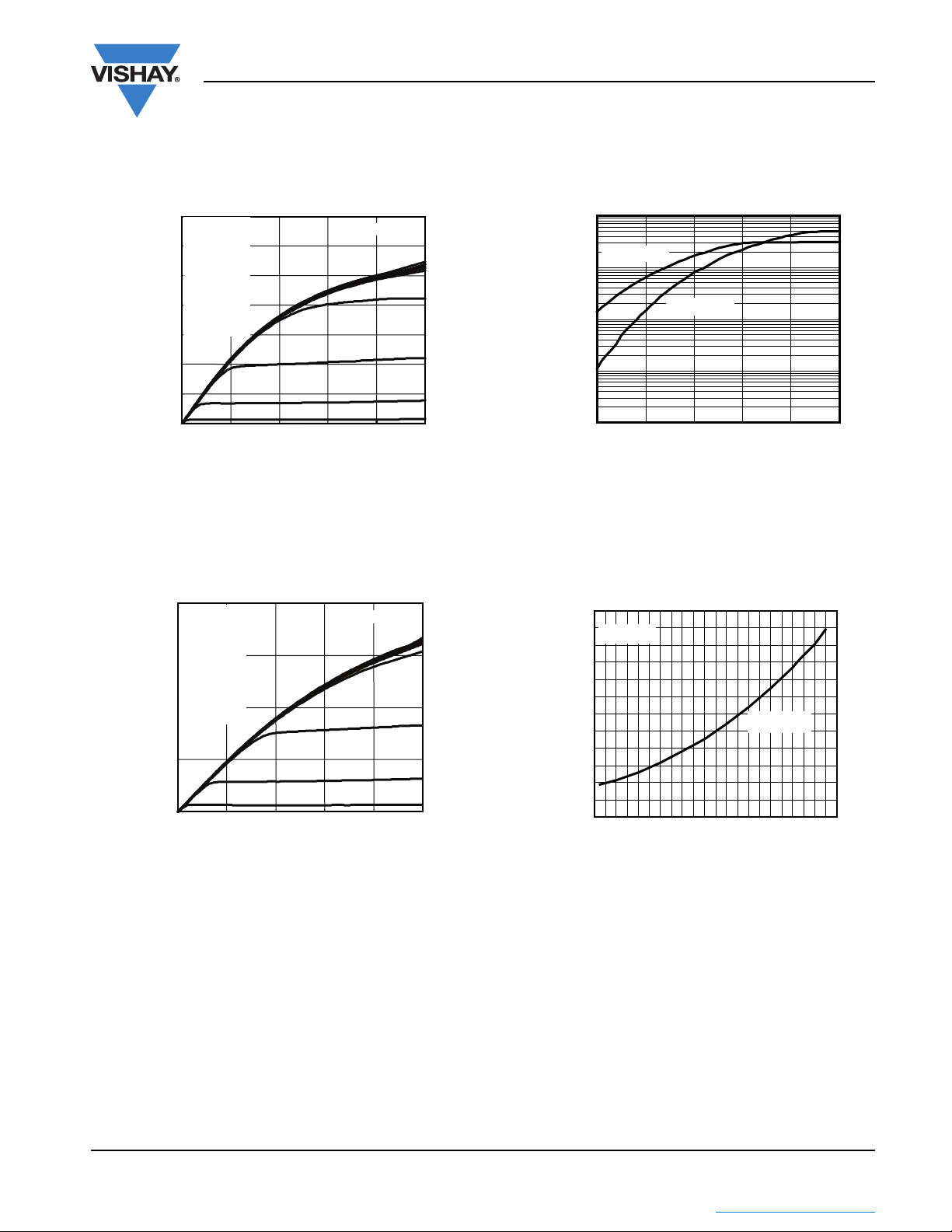
Fig. 1 - Typical Output Characteristics, TC = 150 °C
, Drain Current (A)
D
I
40
30
20
10
0 6 12 18 24 30
To p
Bottom
V
GS
15 V
14 V
13 V
12 V
11 V
10 V
9.0 V
8.0 V
7.0 V
6.0 V
5.0 V
TJ = 150 °C
7.0 V
VDS, Drain-to-Source Voltage (V)
Fig. 2 - Typical Output Characteristics, T
= 150 °C
C
Fig. 3 - Typical Transfer Characteristics
Fig. 4 - Normalized On-Resistance vs. Temperature
Document Number: 91374 www.vishay.com
S11-0520-Rev. D, 21-Mar-11 3
THE PRODUCT DESCRIBED HEREIN AND THIS DATASHEET ARE SUBJECT TO SPECIFIC DISCLAIMERS, SET FORTH AT
This datasheet is subject to change without notice.
www.vishay.com/doc?91000
 Loading...