

Page 1

Integrated DrMOS Power Stage
DESCRIPTION
The SiC769CD is an integrated solution that contains PWM
optimized n-channel MOSFETs (high side and low side) and
a full featured MOSFET driver IC. The device complies with
the Intel DrMOS standard for desktop and server V
stages. The SiC769CD delivers up to 35 A continuous output
current and operates from an input voltage range of 3 V to
16 V. The integrated MOSFETs are optimized for output
voltages in the ranges of 0.8 V to 2.0 V with a nominal input
voltage of 12 V. The device can also deliver very high power
at 5 V output for ASIC applications.
The SiC769CD incorporates an advanced MOSFET gate
driver IC. This IC accepts a single PWM input from the V
controller and converts it into the high side and low side
MOSFET gate drive signals. The driver IC is designed to
implement the skip mode (SMOD) function for light load
efficiency improvement. Adaptive dead time control also
works to improve efficiency at all load points. The SiC769CD
has a thermal warning (THDN) that alerts the system of
excessive junction temperature. The driver IC includes an
enable pin, UVLO and shoot through protection.
The SiC769CD is optimized for high frequency buck
applications. Operating frequencies in excess of 1 MHz can
easily be achieved.
The SiC769CD is packaged in Vishay Siliconix high
performance PowerPAK MLP6 x 6 package. Compact
co-packaging of components helps to reduce stray
inductance, and hence increases efficiency.
core
power
SiC769CD
Vishay Siliconix
FEATURES
•
• Integrated Gen III MOSFETs and DrMOS
compliant gate driver IC
• Enables V
• Easily achieve > 90 % efficiency in multi-phase,
low output voltage solutions
• Low ringing on the VSWH pin reduces EMI
• Pin compatible with DrMOS 6 x 6 version 3.0
• Tri-state PWM input function prevents negative output
voltage swing
• 5 V logic levels on PWM
• MOSFET threshold voltage optimized for 5 V driver bias
R
supply
• Automatic skip mode operation (SMOD) for light load
efficiency
• Under-voltage lockout
• Built-in bootstrap schottky diode
• Adaptive deadtime and shoot through protection
• Thermal shutdown warning flag
• Low profile, thermally enhanced PowerPAK
40 pin package
• Halogen-free according to IEC 61249-2-21 definition
• Compliant to RoHS directive 2002/95/EC
APPLICATIONS
• CPU and GPU core voltage regulation
• Server, computer, workstation, game console, graphics
boards, PC
switching at 1 MHz
core
®
MLP 6 x 6
SiC769CD APPLICATION DIAGRAMM
5 V
V
CIN
SMOD
Controller
PWM
Document Number: 64981
S10-0113-Rev. D, 18-Jan-10
DSBL#
PWM
THDN
SiC769CD
V
VDRV
Gate Driver
C
GND
GH
GL
Figure 1
V
IN
BOOT
V
SWH
PHASE
P
GND
IN
V
O
www.vishay.com
1
Page 2

SiC769CD
Vishay Siliconix
ORDERING INFORMATION
Part Number Packag e
SiC769CD-T1-E3 PowerPAK MLP66-40
SiC769DB Reference board
ABSOLUTE MAXIMUM RATINGS TA = 25 °C, unless otherwise noted
Parameter Symbol Min. Max. Unit
V
V
PWM
THDN
V
V
IN
V
SW
V
DRV
V
CIN
, V
, V
V
BS
BS_PH
T
A
T
J
T
STG
DSBL#
SMOD
- 0.3 20
- 0.3 20
- 0.3 7.0
- 0.3 7.0
,
- 0.3
+ 0.3
V
CIN
V
- 0.3 27
- 0.3 29
- 0.3 7
- 40 125
150
- 65 150
°CStorage Junction Temperature
Input Voltage
Switch Node Voltage (DC)
Drive Input Voltage
Control Input Voltage
Logic Pins
Boot Voltage DC (referenced to C
Boot Voltage < 200 ns Transient (referenced to C
GND
)
)
GND
Boot to Phase Voltage DC
Boot to Phase Voltage < 200 ns - 0.3 9
Ambient Temperature Range
Maximum Junction Temperature
Soldering Peak Temperature 260
Note:
= 25 °C and all voltages referenced to P
a. T
A
GND
= C
unless otherwise noted.
GND
Stresses beyond those listed under "Absolute Maximum Ratings" may cause permanent damage to the device. These are stress ratings only,
and functional operation of the device at these or any other conditions beyond those indicated in the operational sections of the specifications is
not implied. Exposure to absolute maximum rating/conditions for extended periods may affect device reliability.
RECOMMENDED OPERATING CONDITIONS
Parameter Symbol Min. Typ. Max. Unit
Input Voltage V
Control Input Voltage V
Drive Input Voltage V
Switch Node V
SW_DC
IN
CIN
DRV
3.0 12 16
4.5 5.5
4.5 5.5
12 16
V
Note:
a. Recommended operating conditions are specified over the entire temperature range, and all voltages referenced to P
otherwise noted.
GND
= C
GND
unless
THERMAL RESISTANCE RATINGS
Parameter Symbol Typ. Max. Unit
Maximum Power Dissipation at T
Maximum Power Dissipation at T
= 25 °C P
PCB
= 100 °C P
PCB
Thermal Resistance from Junction to Top
Thermal Resistance from Junction to PCB
D_25C
D_100C
R
th_J_TOP
R
th_J_PCB
25
10
15
W
5
°C/W
www.vishay.com
2
Document Number: 64981
S10-0113-Rev. D, 18-Jan-10
Page 3
Vishay Siliconix
ELECTRICAL SPECIFICATIONS
Test Conditions Unless Specified
V
= V
DSBL#
V
= 12 V, V
Parameter Symbol
IN
T
A
Power Supplies
V
= 0 V, no switching 20
DSBL#
V
Control Input Current I
CIN
Drive Input Current (Dynamic) I
VCIN
VDRV
V
DSBL#
= 5 V, no switching 400
DSBL#
= 5 V, fs = 300 kHz, D = 0.1 600
fs = 300 kHz, D = 0.1 11 16
= 1000 kHz, D = 0.1 40 54
f
s
Bootstrap Supply
V
Bootstrap Switch Forward Voltage V
BS Diode
= 5 V, forward bias current 2 mA 0.60 0.75 V
VCIN
Control Inputs (PWM, DSBL#, SMOD)
PWM Rising Threshold V
PWM Falling Threshold V
PWM Tristate Rising Threshold V
PWM Tristate Falling Threshold V
PWM Tristate Rising Threshold Hysteresis V
PWM Tristate Falling Threshold Hysteresis V
Tristate Hold-Off Time
b
PWM Input Current I
SMOD, DSBL# Logic Input Voltage
Pull Down Impedance R
THDN Output Low V
th_pwm_r
th_pwm_f
th_tri_r
th_tri_f
hys_t ri_r
hys_t ri_f
t
TSHO
PWM
V
LOGIC_LH
V
LOGIC_LH
THDN
THDNL
V
PWM
V
PWM
Rising (low to high) 2.0
Falling (high to low) 0.8
5 kΩ resistor pull-up to V
Protection
Thermal Warning Flag Set 150
Thermal Warning Flag Hysteresis 15
Under Voltage Lockout
Under Voltage Lockout Falling, off threshold 2.5 2.9
Under Voltage Lockout Hysteresis V
High Side Gate Discharge Resistor
b
V
UVLO
UVLO_HYST
R
HS_DSCRG
Rising, on threshold 3.3 3.9
V
= V
VDRV
VCIN
Notes:
a. Typical limits are established by characterization and are not production tested.
b. Guaranteed by design.
= 5 V,
SMOD
= V
VDRV
= 25 °C Min. Typ.aMax. Unit
VCIN
5 V,
3.5 3.8 4.2
0.8 1.0 1.2
0.9 1.3 1.8
3.4 3.7 4.0
= 5 V 250
= 0 V - 250
CIN
= 0 V; VIN = 12 V 20.2 kΩ
SiC769CD
µAV
mA
200
300
150 ns
40 Ω
0.04 V
400 mV
mV
µA
V
V
°CThermal Warning Flag Clear 135
V
Document Number: 64981
S10-0113-Rev. D, 18-Jan-10
www.vishay.com
3
Page 4
SiC769CD
Vishay Siliconix
MOSFET SPECIFICATIONS
Test Conditions Unless Specified
V
= V
VCIN
Parameter Symbol
V
High Side
Low Side
R
DS(on)_H
V
R
DS(on)_L
DS
DS
V
VIN
VGS = 0 V, IDS = 250 µA 20 V
VGH = 5 V, resistance measured
VGS = 0 V, IDS = 250 µA 20 V
VGL = 5 V, resistance measured
Note:
a. Typical MOSFET Parameters are provided as a design guide.
TIMING SPECIFICATIONS
Test Conditions Unless Specified
V
VDRV
Parameter Symbol
Turn Off Propagation Delay
High Side
a
Rise Time High Side t
Fall Time High Side t
Turn Off Propagation Delay
Low Side
a
Rise Time Low Side t
Fall Time Low Side t
Dead Time Rising t
Dead Time Falling t
t
d_on_HS
r_HS
f_HS
t
d_off_LS
r_LS
f_LS
dead_on
dead_off
Note:
a. Min. and Max. are not 100 % production tested.
V
VIN
25 % of PWM to 90 % of GH 10 20 30
10 % to 90 % of GH 8
90 % to 10 % of GH 8
75 % of PWM to 90 % of GL 10 20 30
10 % to 90 % of GL 8
90 % to 10 % of GL 8
10 % of GL to 10 % of GH 15
10 % of GH to 10 % of GL 15
DSBL#
= 12 V, TA = 25 °C Min. Typ.aMax. Unit
at package pins
at package pins
= V
= V
VCIN
= 12 V, TA = 25 °C Min. Typ. Max. Unit
= 5 V,
DSBL#
6.0 mΩ
1.7 mΩ
= 5 V,
ns
www.vishay.com
4
Document Number: 64981
S10-0113-Rev. D, 18-Jan-10
Page 5

TIMING DEFINITIONS
PWM
GH
SiC769CD
Vishay Siliconix
75 %
25 %
GL
90 %
10 %
SW
1234 5678
Region Definition Symbol
1 Turn off propagation delay LS t
2 Fall time LS t
3 Dead time rising t
4Rise time HSt
5 Turn off propagation delay HS t
6Fall time HSt
7 Dead time falling t
8 Rise time LS t
Note:
GH is referenced to the high side source. GL is referenced to the low side source.
SiC769CD BLOCK DIAGRAM
90 %
10 %
d_off_LS
f_LS
dead_on
r_HS
d_off_HS
f_HS
dead_off
r_LS
V
CIN
DSBL#
THDN
PWM
SMOD
Document Number: 64981
S10-0113-Rev. D, 18-Jan-10
V
DRV
UVLO
Thermal
Warning
Tristate
PWM
C
GND
AST CNTL
DCM DETECT
GH
GL
V
IN
BOOT
PHASE
VSWH
P
GND
Figure 2
www.vishay.com
5
Page 6

SiC769CD
Vishay Siliconix
DETAILED OPERATIONAL DESCRIPTION
PWM Input with Tristate Function
The PWM input receives the PWM control signal from the V
controller IC. The PWM input is designed to be compatible
with standard controllers using two state logic (H and L) and
advanced controllers that incorporate Tristate logic (H, L and
Tristate) on the PWM output. For two state logic, the PWM
input operates as follows. When PWM is driven above
V
th_pwm_r
on. When PWM input is driven below V
turns off and the Low side turns on. For Tristate logic, the
PWM input operates as above for driving the MOSFETs.
However, there is an third state that is entered into as the
PWM output of Tristate compatible controller enters its high
impedance state during shut-down. The high impedance
state of the controller's PWM output allows the SiC769CD to
pull the PWM input into the Tristate region (see the Tristate
Voltage Threshold Diagram below). If the PWM input stays in
this region for the Tristate Hold-Off Period, t
side and low side MOSFETs are turned off. This function
allows the V
voltage swing caused by inductor ringing and saves a
Schottky diode clamp. The PWM and Tristate regions are
separated by hysteresis to prevent false triggering. The
SiC769CD incorporates PWM voltage thresholds that are
compatible with 5 V logic.
Disable (DSBL#)
In the low state, the DSBL# pin shuts down the driver IC and
disables both high-side and low-side MOSFET. In this state,
the standby current is minimized. If DSBL# is left
unconnected an internal pull-down resistor will pull the pin
down to C
Diode Emulation Mode (SMOD) Skip Mode
When SMOD pin is low the diode emulation mode is enabled.
This is a non-synchronous conversion mode that improves
light load efficiency by reducing switching losses. Conducted
losses that occur in synchronous buck regulators when
inductor current is negative are also reduced. Circuitry in the
gate drive IC detects the inductor valley current when
inductor current crosses zero and automatically stops
switching the low side MOSFET. See SMOD Operation
Diagram for additional details. This function can be also be
used for a pre-biased output voltage. If SMOD is left
unconnected, an internal pull up resistor will pull the pin up to
V
CIN
Thermal Shutdown Warning (THDN)
The THDN pin is an open drain signal that flags the presence
of excessive junction temperature. Connect a maximum of
20 kΩ to pull this pin up to V
sensor detects the junction temperature. The temperature
threshold is 150 °C. When this junction temperature is
exceeded the THDN flag is set. When the junction
temperature drops below 135 °C the device will clear the
THDN signal. The SiC769CD does not stop operation when
the flag is set. The decision to shutdown must be made by an
external thermal control function.
the low side is turned off and the high side is turned
th_pwm_f
phase to be disabled without negative output
R
and shut down the IC.
GND
the high side
TSHO
(Logic High) to disable the SMOD function.
. An internal temperature
CIN
, both high
Voltage Input (V
)
IN
This is the power input to the drain of the high-side Power
R
MOSFET. This pin is connected to the high power
intermediate BUS rail.
Switch Node (V
The Switch node V
and PHASE)
SWH
is the circuit PWM regulated output.
SWH
This is the output applied to the filter circuit to deliver the
regulated high output for the buck converter. The PHASE pin
is internally connected to the switch node V
. This pin is
SWH
to be used exclusively as the return pin for the BOOT
capacitor. A 20.2 kΩ resistor is connected between GH and
PHASE to provide a discharge path for the HS MOSFET in
the event that V
Ground connections (C
(power ground) should be externally connected to
P
GND
C
(control signal ground). The layout of the Printed
GND
goes to zero while VIN is still applied.
CIN
GND
and P
GND
)
Circuit Board should be such that the inductance separating
the C
GND
and P
should be a minimum. Transient
GND
differences due to inductance effects between these two pins
should not exceed 0.5 V.
Control and Drive Supply Voltage Input (V
V
is the bias supply for the gate drive control IC. V
CIN
DRV,VCIN
)
DRV
is
the bias supply for the gate drivers. It is recommended to
separate these pins through a resistor. This creates a low
pass filtering effect to avoid coupling of high frequency gate
drive noise into the IC.
Bootstrap Circuit (BOOT)
The internal bootstrap switch and an external bootstrap
capacitor form a charge pump that supplies voltage to the
BOOT pin. An integrated bootstrap diode is incorporated so
that only an external capacitor is necessary to complete the
bootstrap circuit. Connect a boot strap capacitor with one leg
tied to BOOT pin and the other tied to PHASE pin.
Shoot-Through Protection and Adaptive Dead Time
(AST)
The SiC769CD has an internal adaptive logic to avoid shoot
through and optimize dead time. The shoot through
protection ensures that both high-side and low-side
MOSFET are not turned on the same time. The adaptive
dead time control operates as follows. When PWM input
goes high the LS gate starts to go low after a few ns. When
this signal crosses through 1.7 V the logic to switch the HS
gate on is activated. When PWM goes low the HS gate goes
low. When the HS gate-to-source drive signal crosses
through 1.7 V the logic to turn on the LS gate is activated.
This feature helps to adjust dead time as gate transitions
change with respect to output current and temperature.
Under Voltage Lockout (UVLO)
During the start up cycle, the UVLO disables the gate drive
holding high-side and low-side MOSFET gate low until the
input voltage rail has reached a point at which the logic
circuitry can be safely activated. The SiC769CD also
incorporates logic to clamp the gate drive signals to zero
when the UVLO falling edge triggers the shutdown of the
device. As an added precaution, a 20.2 kΩ resistor is
connected between GH and PHASE to provide a discharge
path for the HS MOSFET.
www.vishay.com
6
Document Number: 64981
S10-0113-Rev. D, 18-Jan-10
Page 7

DEVICE TRUTH TABLE
DSBL# SMOD PWM GH GL
Open
L
H
H
H
H
XXL L
XXL L
LLLH (I
LHHL
HHHL
HLLH
TRISTATE PWM VOLTAGE THRESHOLD DIAGRAM
SiC769CD
Vishay Siliconix
> 0), L (IL ≤ 0)
L
V
th_pwm_r
V
th_tri_f
V
th_tri_r
V
th_pwm_f
PWM
GH
GL
SMOD OPERATION DIAGRAM
DSBL
SMOD
PWM
GH
GL
t
TSHO
t
TSHO
Figure 3
= 0
I
> 0
I
L
L
Document Number: 64981
S10-0113-Rev. D, 18-Jan-10
VSW
t
d(ON)
t
d(OFF)
Figure 4
www.vishay.com
7
Page 8

SiC769CD
Vishay Siliconix
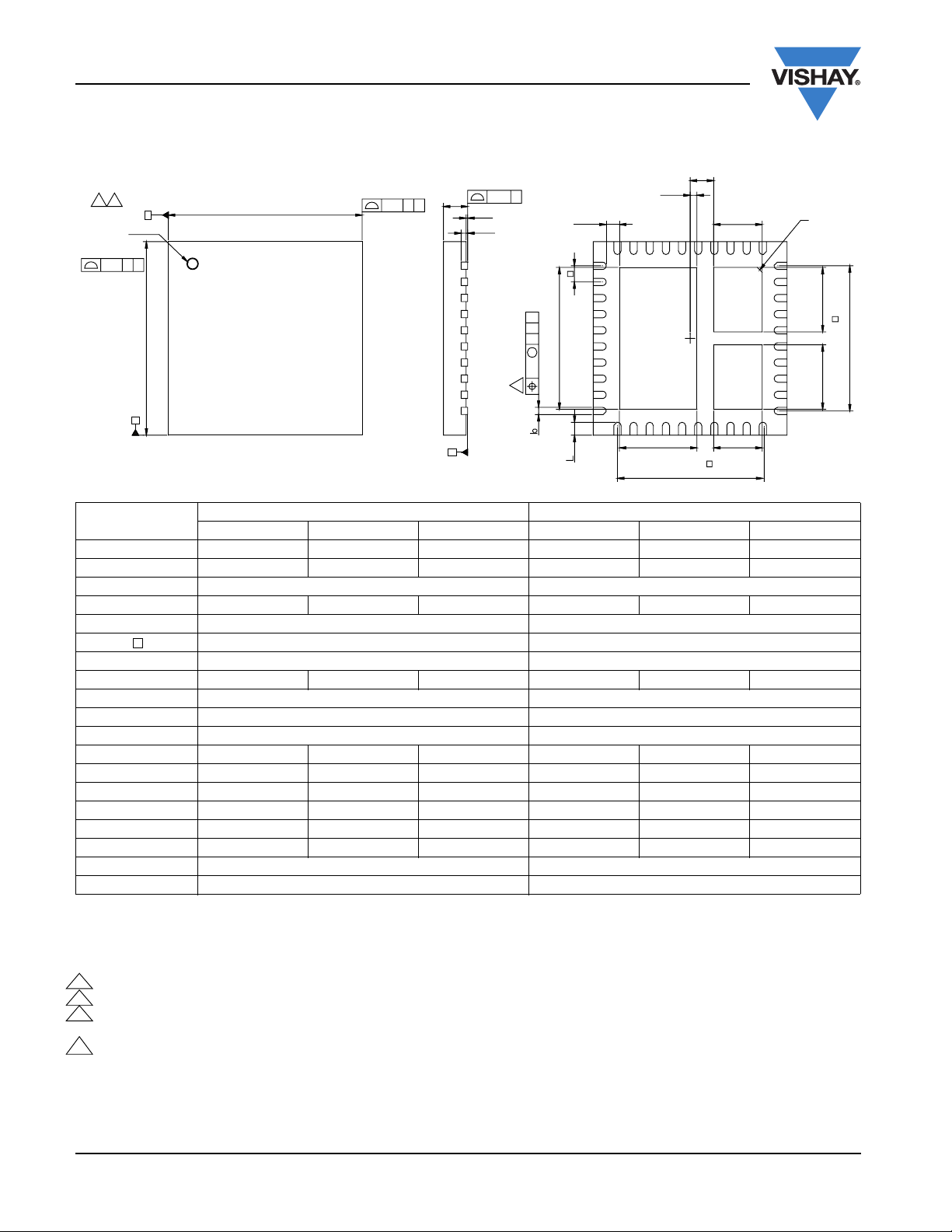
PIN CONFIGURATION
39 DSBL#
40 PWM
GND
32 VSWH
37 C
38 THDN
36 GL
35 VSWH
34 VSWH
31 VSWH
33 VSWH
20 P
G
N
D
30 VSWH
29 VSWH
28 P
GND
27 P
GND
26 P
GND
25 P
GND
24 P
GND
23 P
GND
22 P
GND
21 P
GND
SMOD 1
V
CIN
V
DRV
BOOT 4
C
GND
GH 6
PHASE 7
V
IN
V
IN
10
V
IN
2
3
5
8
9
A
GND
P1
VSWH
P3
V
IN
P2
16 P
15
11 V
IN
14 VIN13 VIN12 V
I
N
V
SWH
G
ND
17 P
G
N
D
19 P
18
P
G
G
N
ND
D
Figure 5 - PowerPAK MLP 6 x 6 40P Pin Out - Top View
PIN DESCRIPTION
Pin Number Symbol Description
1 SMOD Disable low side gate operation. Active low.
2V
3V
CIN
DRV
4 BOOT High side driver bootstrap voltage pin for external bootstrap capacitor.
5, 37, PAD1 C
GND
6 GH Gate signal output pin for high side MOSFET. Pin for monitoring.
7 PHASE Return pin for the HS bootstrap capacitor. Connect a 0.1 µF ceramic capacitor from this pin to the boot pin (4).
8 to 14, PAD2 V
15, 29 to 35,
PA D3
16 to 28 P
VSWH
GND
36 GL Gate signal output pin for low side MOSFET. Pin for monitoring.
38 THDN Thermal shutdown open drain output. Use a 10K pull up resistor to V
39 DSBL# Disable pin. Active low.
40 PWM PWM input logic signal. Compatible with Tristate controller function.
This will be the bias supply input for control IC (5 V).
IC bias supply and gate drive supply voltage (5 V).
Control signal ground. It should be connected to P
Input voltage for power stage. It is the drain of the high-side MOSFET.
IN
externally. All pins internally connected.
GND
It is the phase node between high side MOSFET source and low side MOSFET drain. It should be connected
to an output inductor. All pins internally connected.
Power ground.
.
CIN
www.vishay.com
8
Document Number: 64981
S10-0113-Rev. D, 18-Jan-10
Page 9

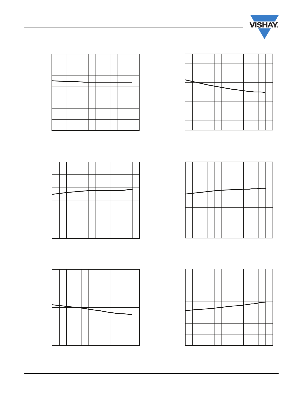
ELECTRICAL CHARACTERISTICS
1.0
SiC769CD
Vishay Siliconix
20
0.8
0.6
(mA)
CIN
I
0.4
0.2
0.0
- 40 - 25 - 10 5 20 35 50 65 8095110125140
Temperature (°C)
I
(mA) vs. Temperature at Frequency = 300 kHz
(V)
SH
PWM T
CIN
1.3
1.2
1.1
1.0
0.9
D = 10 %, V
CIN
= V
DRV
= 5 V
18
16
14
(mA)
12
DRV
I
10
8
6
- 40 - 25 - 10 5 20 35 50 65 80 95 110 125 140
Temperature (°C)
I
(mA) vs. Temperature at Frequency = 300 kHz
(V)
SH
PWM T
DRV
4.4
4.2
4.0
3.8
3.6
3.4
3.2
D = 10 %, V
CIN
= V
DRV
= 5 V
0.8
- 40 - 25 - 10 5 20 35 50 65 80 95 110 125 140
PWM Falling Threshold (V) vs. Temperature (°C)
1.6
1.5
1.4
(V)
1.3
SH
1.2
DSBL T
1.1
1.0
0.9
- 40 - 25 - 10 5 20 35 50 65 80 95 110 125 140
DSBL Falling Threshold (V) vs. Temperature (°C)
Document Number: 64981
S10-0113-Rev. D, 18-Jan-10
Temperature (°C)
V
= V
= V
DRV
DRV
= 5 V
= 5 V
CIN
Temperature (°C)
V
CIN
3.0
- 40 - 25 - 10 5 20 35 50 65 80 95 110 125 140
Temperature (°C)
PWM Rising Threshold (V) vs. Temperature (°C)
V
= V
DRV
= 5 V
CIN
1.80
1.75
1.70
1.65
(V)
SH
1.60
DSBL T
1.55
1.50
1.45
1.40
- 40 - 25 - 10 5 20 35 50 65 80 95 110 125 140
Temperature (°C)
DSBL Rising Threshold (V) vs. Temperature (°C)
V
= V
DRV
= 5 V
CIN
www.vishay.com
9
Page 10
SiC769CD
Vishay Siliconix
ELECTRICAL CHARACTERISTICS
1.6
1.80
1.5
1.4
(V)
1.3
SH
1.2
SMOD T
1.1
1.0
0.9
- 40 - 25 - 10 5 20 35 50 65 80 95 110 125 140
Temperature (°C)
SMOD Falling Threshold (V) vs. Temperature (°C)
V
= V
DRV
= 5 V
(mA)
CIN
I
CIN
60
50
40
30
20
1.75
1.70
1.65
(V)
SH
1.60
1.55
SMOD T
1.50
1.45
1.40
- 40 - 25 - 10 5 20 35 50 65 80 95 110 125 140
Temperature (°C)
SMOD Rising Threshold (V) vs. Temperature (°C)
V
= V
DRV
= 5 V
(mA)
DRV
I
CIN
50
45
40
35
10
0
- 40 - 25 - 10 5 20 35 50 65
Temperature (°C)
I
+ I
(mA) vs. Temperature at Frequency = 1 MHz
DRV
D = 10 %, V
1.6
1.5
1.4
1.3
1.2
1.1
1.0
- 40 - 25 - 10 5 20 35 50 65 80 95 110 125 140
CIN
Temperature (°C)
(V)
SH
PWM T
CIN
80 95 110 125 140
= V
= 5 V
DRV
PWM Falling Tristate (V) vs. Temperature (°C)
V
= V
DRV
= 5 V
CIN
30
25
- 40 - 25 - 10 5 20 35 50 65
Temperature (°C)
I
(mA) vs. Temperature at Frequency = 1 MHz
DRV
4.4
4.2
4.0
(V)
3.8
SH
3.6
PWM T
3.4
3.2
3.0
- 40 - 25 - 10 5 20 35 50 65 80 95 110 125 140
D = 10 %, V
Temperature (°C)
CIN
80 95 110 125 140
= V
= 5 V
DRV
PWM Rising Tristate Threshold (V) vs. Temperature (°C)
V
= V
DRV
= 5 V
CIN
www.vishay.com
10
Document Number: 64981
S10-0113-Rev. D, 18-Jan-10
Page 11

ELECTRICAL CHARACTERISTICS
2.5
2.3
2.1
1.9
1.7
(V)
SH
1.5
1.3
DSBL T
1.1
0.9
0.7
0.5
4.7 4.8 4.9 5.0 5.1 5.2 5.3 5.4 5.5 5.6
V
(V)
CIN
DSBL Falling Threshold vs. V
CIN
SiC769CD
Vishay Siliconix
2.5
2.3
2.1
1.9
1.7
(V)
SH
1.5
1.3
DSBL T
1.1
0.9
0.7
0.5
4.7 4.8 4.9 5.0 5.1 5.2 5.3 5.4 5.5 5.6
V
(V)
CIN
DSBL Rising Threshold vs. V
CIN
2.5
2.3
2.1
1.9
1.7
(V)
SH
1.5
1.3
DSBL T
1.1
0.9
0.7
0.5
4.7 4.8 4.9 5.0 5.1 5.2 5.3 5.4 5.5 5.6
V
(V)
CIN
SMOD Falling Threshold vs. V
1.15
1.10
1.05
(V)
SH
1.00
PWM T
0.95
CIN
2.5
2.3
2.1
1.9
(V)
1.7
SH
1.5
1.3
SMOD T
1.1
0.9
0.7
0.5
4.7 4.8 4.9 5.0 5.1 5.2 5.3 5.4 5.5 5.6
V
(V)
CIN
SMOD Rising Threshold vs. V
4.4
4.2
4.0
(V)
3.8
SH
3.6
PWM T
3.4
3.2
CIN
0.90
4.7 4.8 4.9 5.0 5.1 5.2 5.3 5.4 5.5 5.6
PWM Falling Threshold vs. V
Document Number: 64981
S10-0113-Rev. D, 18-Jan-10
3.0
4.7 4.8 4.9 5.0 5.1 5.2 5.3 5.4 5.5 5.6
V
V
(V)
CIN
CIN
PWM Rising Threshold vs. V
CIN
(V)
CIN
www.vishay.com
11
Page 12

SiC769CD
Vishay Siliconix
ELECTRICAL CHARACTERISTICS
V
V
lind
V
OUT
V
OUT
V
CIN
= 30 A
SMOD
IN
OUT
= 1.2 V,
IN
V
OUT
CIN
Startup at VIN = 12 V, V
F
= 1 MHz, I
S
SMOD
OUT
= 1.2 V,
OUT
= 30 A
lind
Power Off at VIN = 12 V, V
F
= 1 MHz, I
S
V
SW
Disable SMOD at V
V
SW
GH
GL
PWM
Driver Performance at V
IN
F
= 1 MHz, I
S
= 12 V, V
IN
OUT
= 1.2 V, FS = 1 MHz
OUT
= 12 V, V
OUT
= 10 A
= 1.2 V,
V
SW
Enable SMOD at V
V
SW
GH
PWM
GL
Driver Performance at V
= 12 V, V
IN
F
= 1 MHz, I
S
= 1.2 V, FS = 1 MHz
OUT
= 12 V, V
IN
OUT
OUT
= 10 A
= 1.2 V,
www.vishay.com
12
Document Number: 64981
S10-0113-Rev. D, 18-Jan-10
Page 13

TYPICAL POWER LOSS IN SIC769CD PowerPAK MLP66-40 PACKAGE
9
8
7
6
5
4
3
Package Dissipation (W)
2
1
0
0 5 10 15 20 25 30 35 40
= 12 V, V
V
IN
IHLP5050EZ-01 Inductor: 1 MHz = 220 nH; 300 kHz = 470 nH
P
LOSS_PKG
Figure 6 - SiC769CD PowerPAK MLP66-40 Package
= 1.2 V, V
OUT
= P
1 MHz
VCIN
I
OUT
+ P
DRV
(A)
VDRV
= V
CIN
+ P
300 kHz
= 5 V; No Air Flow
- P
VIN
OUT_VSW
SiC769CD
Vishay Siliconix
TYPICAL EFFICIENCY CURVES
Efficiency (%)
95
90
500 kHz
300 kHz
85
1 MHz
80
75
70
0 5 10 15 20 25 30 35 40
I
(A)
OUT
= 12 V, V
V
IN
IHLP5050EZ-01 Inductor: 1 MHz = 220 nH, 0.8 mΩ;
= 1.2 V, V
OUT
DRV
= V
= 5 V; No Air Flow
CIN
500 kHz = 330 nH, 1.1 mΩ; 300 kHz = 470 nH, 1.3 mΩ
/(P
+ P
Efficiency % = 100 x P
VOUT
VCIN
VDRV
+ P
Figure 7
VIN
)
Document Number: 64981
S10-0113-Rev. D, 18-Jan-10
www.vishay.com
13
Page 14
SiC769CD
Vishay Siliconix
PACKAGE DIMENSIONS
56
Pin 1 dot
by marking
2 x
0.10 C B
A
D
2 x
0.10 C A
K1
0.08 C
A
A1
A2
0.41
31
30
e
K2
D2-1
Pin #1 dent
40
1
MLP66-40
(6 mm x 6 mm)
C A B
E2-1
M
0.10
4
21
1120
D2-2
e
Top View
C
Side View
D2-3
(Nd-1)X
ref.
Bottom View
MILLIMETERS INCHES
Min. Nom. Max. Min. Nom. Max.
0.70 0.75 0.80 0.027 0.029 0.031
10
B
DIM
A
E
(8)
A1 0.00 - 0.05 0.000 - 0.002
A2 0.20 ref. 0.008 ref.
(4)
b
0.20 0.25 0.30 0.078 0.098 0.011
D 6.00 BSC 0.236 BSC
e 0.50 BSC 0.019 BSC
E 6.00 BSC 0.236 BSC
L 0.35 0.40 0.45 0.013 0.015 0.017
N
Nd
Ne
(3)
(3)
(3)
40 40
10 10
10 10
D2-1 1.45 1.50 1.55 0.057 0.059 0.061
D2-2 1.45 1.50 1.55 0.057 0.059 0.061
D2-3 2.35 2.40 2.45 0.095 0.094 0.096
E2-1 4.35 4.40 4.45 0.171 0.173 0.175
E2-2 1.95 2.00 2.05 0.076 0.078 0.080
E2-3 1.95 2.00 2.05 0.076 0.078 0.080
K1 0.73 BSC 0.028 BSC
K2 0.21 BSC 0.008 BSC
Notes:
1. Use millimeters as the primary measurement.
2. Dimensioning and tolerances conform to ASME Y14.5M-1994.
3. N is the number of terminals.
Nd is the number of terminals in X-direction and Ne is the number of terminals in Y-direction .
4. Dimension b applies to plated terminal and is measured between 0.20 mm and 0.25 mm from terminal tip.
5. The pin #1 identifier must be existed on the top surface of the package by using indentation mark or other feature of package body .
6. Exact shape and size of this feature is optional.
7. Package warpage max. 0.08 mm.
8. Applied only for terminals.
Figure 8 - PowerPAK MLP 66-40
E2-2
E2-3
e
ref.
(Nd-1)X
www.vishay.com
14
Document Number: 64981
S10-0113-Rev. D, 18-Jan-10
Page 15

LAND PATTERN DIMENSIONS
1
1
SiC769CD
Vishay Siliconix
1.700
2.600
2.200
0.276
0.320
0.310
4.600
0.200
2.200
0.276
40
Figure 9 - PowerPAK MLP 66-40
TAPE AND REEL CARRIER TAPE DIMENSIONS
+ 0.1
Ø 1.5
- 0.0
12.00
0.30 ± 0.05
2.00 ± 0.10 see note 3
4.00 see note 1
0.100
0.100
0.100
0.100
Ø 1.50 min.
0.025
0.600
0.100
0.100
0.100
0.100
0.100
0.100
A
0.025
40
1.75 ± 0.1
R 0.3 max.
Section A-A
B
o
A
K
o
A
o
0.25
Ao = 6.30
Bo = 6.30
Ko = 1.10
R 0.25
7.5 ± 0.1
see note 3
16.0 ± 0.3
Notes:
1. 10 sprocket hole pitch cumulative tolerance ± 0.2.
2. Camber in compliance with EIA 481.
3. Pocket position relative to sprocket hole measured as true position of pocket, not pocket hole.
Figure 10 - PowerPAK MLP 66-40
Vishay Siliconix maintains worldwide manufacturing capability. Products may be manufactured at one of several qualified locations. Reliability data for Silicon
Technology and Package Reliability represent a composite of all qualified locations. For related documents such as package/tape drawings, part marking, and
reliability data, see www.vishay.com/ppg?64981
.
Document Number: 64981
S10-0113-Rev. D, 18-Jan-10
www.vishay.com
15
Page 16

Legal Disclaimer Notice
Vishay
Disclaimer
All product specifications and data are subject to change without notice.
Vishay Intertechnology, Inc., its affiliates, agents, and employees, and all persons acting on its or their behalf
(collectively, “Vishay”), disclaim any and all liability for any errors, inaccuracies or incompleteness contained herein
or in any other disclosure relating to any product.
Vishay disclaims any and all liability arising out of the use or application of any product described herein or of any
information provided herein to the maximum extent permitted by law. The product specifications do not expand or
otherwise modify Vishay’s terms and conditions of purchase, including but not limited to the warranty expressed
therein, which apply to these products.
No license, express or implied, by estoppel or otherwise, to any intellectual property rights is granted by this
document or by any conduct of Vishay.
The products shown herein are not designed for use in medical, life-saving, or life-sustaining applications unless
otherwise expressly indicated. Customers using or selling Vishay products not expressly indicated for use in such
applications do so entirely at their own risk and agree to fully indemnify Vishay for any damages arising or resulting
from such use or sale. Please contact authorized Vishay personnel to obtain written terms and conditions regarding
products designed for such applications.
Product names and markings noted herein may be trademarks of their respective owners.
Document Number: 91000 www.vishay.com
Revision: 18-Jul-08 1
 Loading...