12-V VCM/Spindle Motor Driver for Large Capacity HDD
FEATURES
• 12-V Motor Supply
• Blocking Schottky Diode Replaced by External Synchronous Rectifier
• Spindle Motor Driver Features:
– External LITTLE FOOT® Drivers for High Current/Power Application
– Constant Off-Time PWM Current Drive Mini mizin g Powe r Diss ip ati on
– Sensorless Motor Commutation Immune to PWM Noise
– Externally Controlled Start-Up/Run Function
– Low-Jitter Commutation Output for External Speed Control
– Level Shifting Buffer Amplifier for PWM DAC
– Adjustable Output Slew Rate Control
– Unique Commutation Driver Minimizing Audible Noise
– Programmable Phase Advance for High Speed Motor
– Speed Triggered Motor Brake for Enhanced Reliability
• Voice Coil Motor Driver Features:
– External LITTLE FOOT Drivers for High Current/Power Application
– Low Crossover Distortion in Linear Mode (Class AB)
– Selectable Constant Frequency PWM or Linear Operation
– Programmable Retract Voltage Clamp
– Level Shifting Buffer Amplifier for PWM DAC
– Direct VCM Retract Control Input
– Current Sense Output for Enhanced Servo Control
– Fixed PWM Output Slew Rate Limit
• System Manager Features:
– Power-On Reset Generator
– Adjustable System Voltage Monitor
– 2.3/5.0-V±5%, 150 ppm/°C Reference Output for External PWM DAC
– Programmable Timer for Head Retract and Spindle Brake Delay
– Built-In Test Ability
• 3-Wire Synchronous Serial Data Interface
• Internal Registe rs and Ad dress Dec oding w ith Full Readback Capabi lity
Si9993CS
Vishay Siliconix
Si9993
DESCRIPTION
The Si9993CS consists of a 3-phase brushless dc motor
(spindle) PWM controll er an d a li nea r/PWM transconductance
stage suitable for driving a voice coil motor (head actuator). T o
meet the power handling capability required for a high
capacity hard disk drive, both drivers utilize external LITTLE
FOOT half-bridges (Siliconix Si9942 recommended). A
separate LITTLE FOOT PMOS switch (Si9430) is used as a
FaxBack 408-970-5600, request 70653 S-60752–Rev. A, 05-Apr-99
www.siliconix.com 1
synchronous r ectifier in place of the usual Scho ttky blocking
diode.
Si9993CS is manufactured in a junction-isolated BiC/DMOS
process (JIBCD15) and is available in a 64-pin SQFP
package, specified to operate over the commercial (0°C to
70°C) temperature range.

Si9993CS
Vishay Siliconix
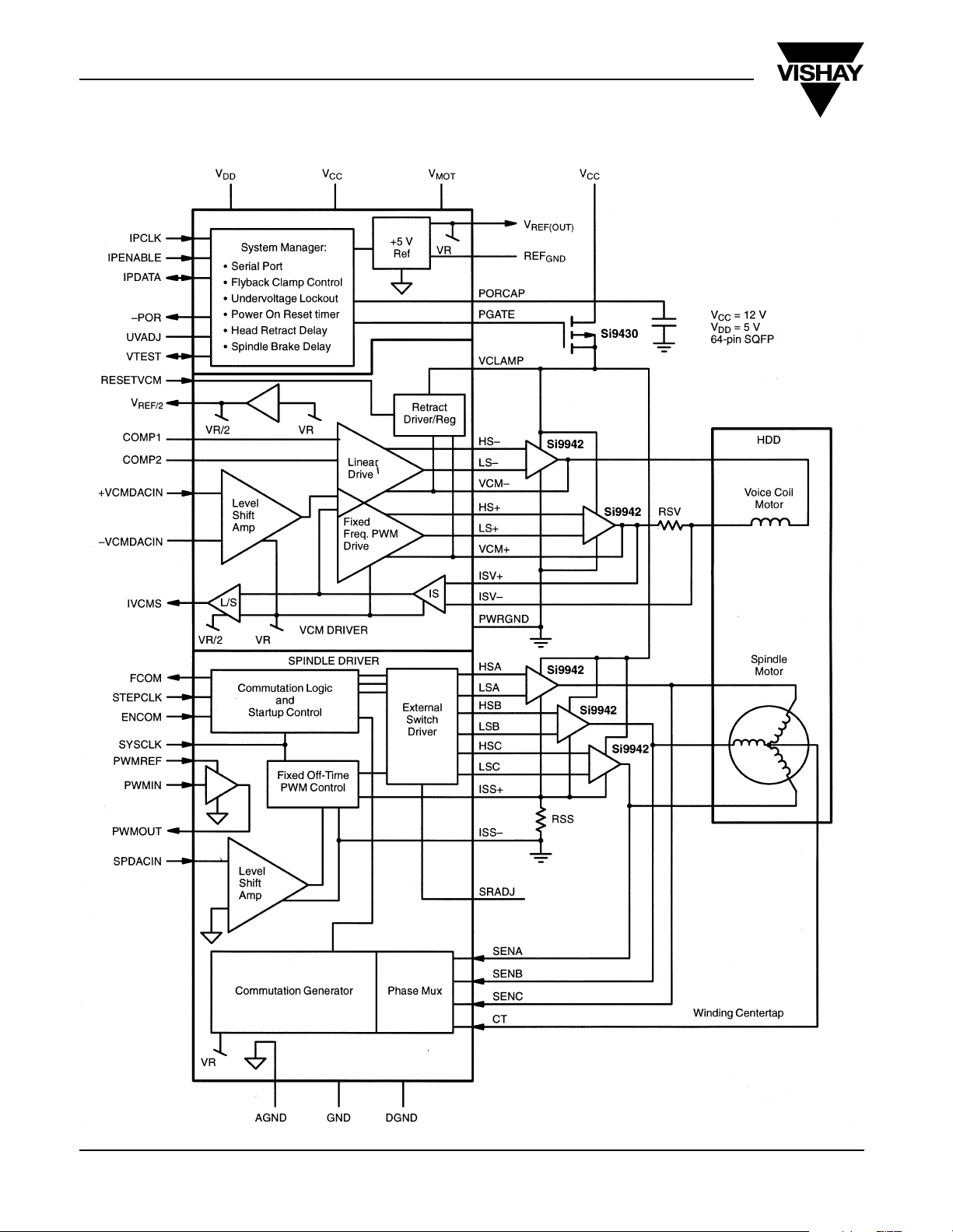
FUNCTIONAL BLOCK DIAGRAM
S-60752–Rev. A, 05-Apr-99 FaxBack 408-970-5600, request 70653
2 www.siliconix.com

Si9993CS
Vishay Siliconix
ABSOLUTE MAXIMUM RATINGS (TA = 25°C)*
Voltage Referenced to GND Pin
Supply Range. . . . . . . . . . . . . . . . . . . . . . . . . . . . . . . .-0.3 to 7 V
V
DD
Supply Range. . . . . . . . . . . . . . . . . . . . . . . . . .> (VCC - 0.3 V
V
CLAMP
V
CC
and > (V
, V
Supply Range . . . . . . . . . . . . . . . . . . . . . . . . .-0.3 to 14 V
MOT
- 0.3 V) to 14 V
DD
AGND, DGND, PWRGND to GND. . . . . . . . . . . . . . . . . . -0.3 to 0.3 V
SENA, SENB, SENC, CT, VCM+, VCM-Pin . . . . .-1.0 to V
, FCOM, STEPCLK, ENCOM , SY SCLK, PWMIN,
POR
+ 1.0 V
CC
PWMOUT, RESETVCM, IPCLK, IPDATA
and IPENABLE pins . . . . . . . . . . . . . . . . . . . . . . .-0.3 to V
* Exposure to Absolute Maximum rating conditions for extended periods may affect device reliability. Stresses above Absolute Maximum rating may cause
permanent dama ge. Functional op eration at conditi ons other than th e operating conditio ns specified is not i mplied. Only on e Absolute Maximum rating should be
applied at any one time. Device mounted on one-inch square FR4 Board.
+ 0.3 V
DD
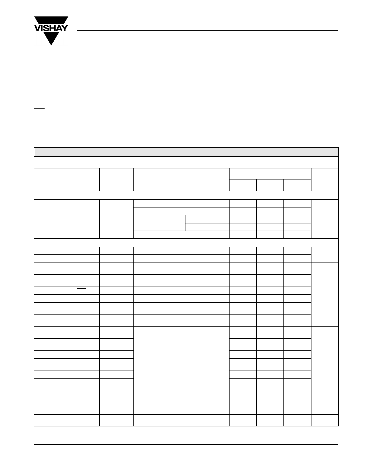
SPECIFICATIONS
Operating Conditions:
VCC = V
R
SRADJ
Parameter Symbol Specific Test Conditions
Power Suppl y
Supply Current
I
CC
Control Logic
Low Input Current I
High Input Current I
Low Input Voltage
(All Digital Inputs)
High Input Voltage
(All Digital Inputs)
Low Output Voltage (POR
High Output Voltage (POR
Low Output Voltage
(FCOM, PWMOU T )
High Output Voltage
(FCOM, PWMOU T )
IPDATA Setup Time to Rising
IPCLK Edge
Rising IPCLK Edge to IPDATA
Hold Time
IPDATA Clock Cycle Time t
IPDATA Hold for IPDATA Driver
Turnaround
IPCLK High and Low Time t
IPDATA Propagation Delay
WRT IPCLK Falling Edge
IPENABLE Setup Time WRT
IPCLK Rising Edge
IPENABLE Hold Time WRT
IPCLK Rising Edge
WRT IPCLK Falling Edge to
Data Tri-State
)V
)V
= 12 V ±10%, VDD = 5 V ±10%, V
MOT
= 20 kΩ ±1%, Si9942-Si9430 LITTLE FOOT Driver, F
I
DD
+ I
I
CLAMP
IL
IH
V
V
OL
OH
V
OL
V
OH
t
t
t
t
t
t
t
MOT
IL
IH
1
2
3
4
5
6
7
8
9
+
Normal Operation, Serial Port Idle 0.2 1.2
D7D6(REG0/5) = 00, All Clocks Disabled 0.02 0.1
Normal Operation
No Load at V
D7D6(REG0/5) = 00, All Clocks Disabled 4 6
REF(OUT)
VIN = V
I
OUT
I
OUT
I
OUT
I
OUT
See Timing Diagram, Figures 1 and 2.
See Timing Diagram, Figures 1 and 2. 10 ns
All Other Pins . . . . . . . . . . . . . . . . . . . . . . . . . . . . -0.3 to V
Maximum Current (All Input Pins). . . . . . . . . . . . . . . . . . . . . .±20 mA
Storage Temperatur e (T
Operating Temperature (T
Junction Temperature (T
). . . . . . . . . . . . . . . . . . . . . . . -65 to 150°C
stg
) . . . . . . . . . . . . . . . . . . . . . . . . .0 to 70°C
A
). . . . . . . . . . . . . . . . . . . . . . . . . . . . . 150°C
J
Power Dissipation . . . . . . . . . . . . . . . . . . . . . . . . . . . . . . . . . . . . . 2 W
Thermal Impedance (
REF(IN)
= V
, RSS = RSV = 0.2 Ω ±1%,
REF(OUT)
SYSCLK
). . . . . . . . . . . . . . . . . . . . . . . . . . 6.25°C/W
Θ
JA
= 5 MHz, TA = 0 to 70°C
Limits
a
With VCM Load 40 65
Without VCM Load 25 40
VIN = 0 V -1
DD
2.0
= 4 mA 0.4
= -4 mA 4.1
= 2 mA 0.4
= -2 mA 4.1
15
15
100
70
45
100
20
Typ
b
Max
1
0.8
100
+ 0.3 V
CC
a
UnitMin
mA
µA
V
ns
FaxBack 408-970-5600, request 70653 S-60752–Rev. A, 05-Apr-99
www.siliconix.com 3

Si9993CS
Vishay Siliconix
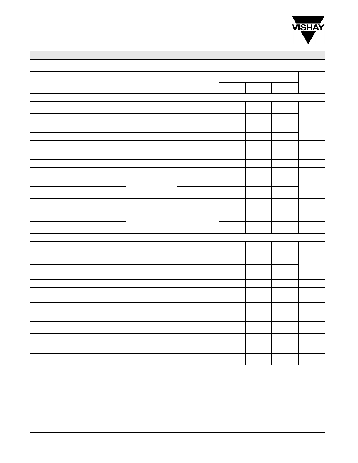
SPECIFICATIONS
Operating Conditions:
VCC = V
R
SRADJ
Parameter Symbol Specific Test Conditions
System Manager
VDD Undervoltage Detection
Threshold (High-to-Low)
VDD Hysteresis 0.05
VCC Undervoltage Detection
Threshold (High-to-Low)
VCC Hysteresis 0.2
POR Time-out t
Delay Time from PWR Failure
to POR Active
POR Charging Current I
POR Comparator Hysteresis 1.0 V
Adjustable Internal Spindle
Brake Delay Time
Internal VCM Retract Delay
Time
Leakage I
V
TEST
5-V Reference Initial P ower-On
T olerance
5-V Reference Drift from Initial
Power-On To lerance
VCM Driver
Transconductance G
Output Offset Current I
DAC Reference Output V
VCMDACIN Input Range +VCMDACIN or -VCMDACIN to GND 0.1 5.0
VCMDACIN Input Bias Current I
Feedback Resistance R
3-dB Bandwidth
CMRR of Current Sense
Amplifier
Head Retract Voltage Clamp I
Short Circuit Head Retract
Current
Current Sense Amplifier Zero
Output Voltage
Current Sense Amplifier
Output Gain Ratio
V(IVCMS)
V(IVCMS)/
= 12 V ±10%, VDD = 5 V ±10%, V
MOT
= 20 kΩ ±1%, Si9942-Si9430 LITTLE FOOT Driver, F
REF(IN)
= V
, RSS = RSV = 0.2 Ω ±1%,
REF(OUT)
= 5 MHz, TA = 0 to 70°C
SYSCLK
Limits
a
Unconnected 4.500 4.625 4.750
UV
ADJ
8.5 9.25 10.0
POR
t
POR
POR
t
spindly
t
vcmdly
VTEST
V
REF
V
∆
REF
---------------- -
V
REF
mVCM
OS
REF/2
(L/S) 50 nA
b
FB
V
CLAMP
V
V
REF(IN)
Internal Resistor from IVCMS to COMP1 12 k
PORCAP = 0.5 µF 350 500 650 ms
= 3.0 to 13.2 V
= VCC = 0 V
DD
V
= 3.0 V, VDD = VCC = 0 V
CLAMP
V
TEST
= V
REF(OUT)
= 20 mA to -2 mA
I
OUT
I
= 1 A, D5D4(REG0) = 11 1.52 1.60 1.68 A/V
MOTOR
D3D2(REG1) = 01 192
D5D4(REG1) = 01 8
= 10 V
(Internal Reference)
4.75 5.00 5.25 V
-1.5 1.5 %
D5D4(REG0) = 11 -25 0 25 mA
R
LOAD
= 100 k
Ω
2.09 2.2 2.31
L/S, I/S and Comp Amp 1.0
Class B Power Amp 0.4
CM Input = 0 to V
= 60 mA, D7D6(REG1) = 00 0.32 0.4 0.48 V
MOTOR
CC
120 180 mA
= 0
I
D7D6(REG0) = 00, D7D6(REG5) = 11
D7D6(REG0) = 00, D7D6(REG5) = 11
V(RSV)
MOTOR
I
MOTOR
= 0
2.32 2.5 2.68 V
dc Gain 2.67 V/V
Typ
b
Max
a
0.8 1.0 µS
2µA
1µA
70 dB
UnitMin
V
ms
V
Ω
MHz
S-60752–Rev. A, 05-Apr-99 FaxBack 408-970-5600, request 70653
4 www.siliconix.com

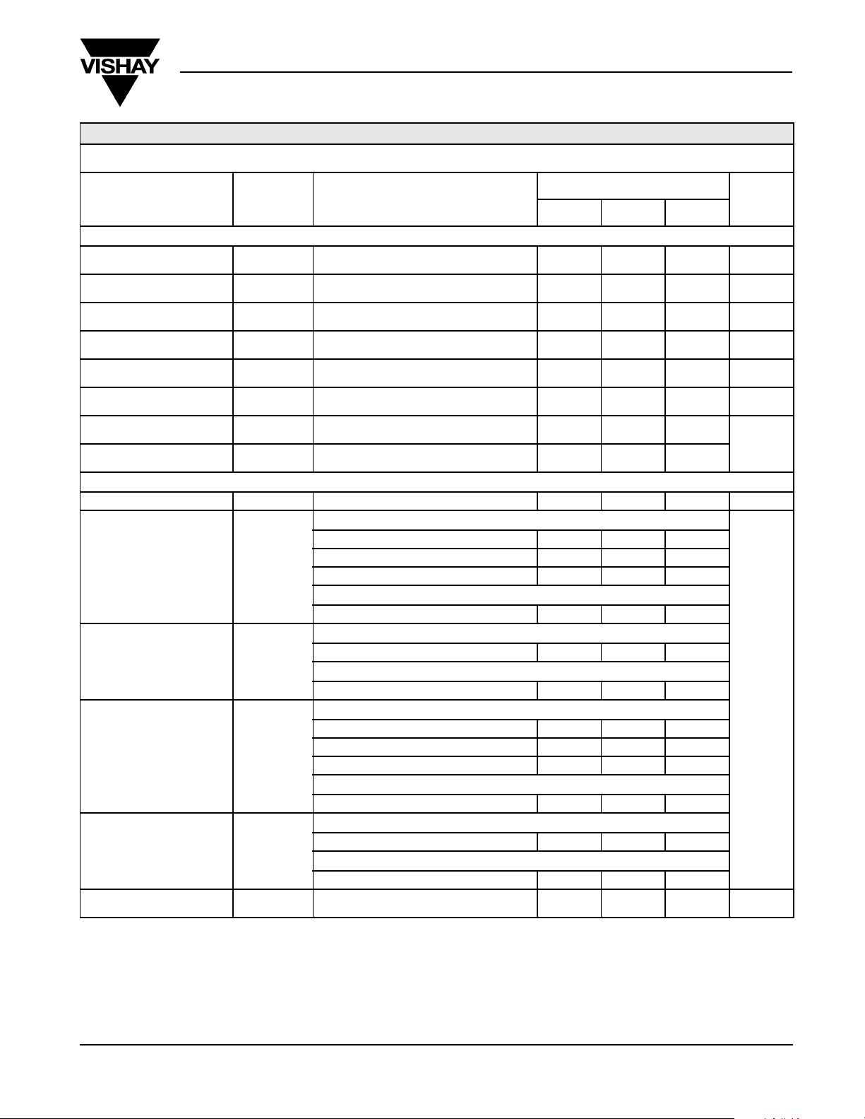
SPECIFICATIONS
Operating Conditions:
VCC = V
R
SRADJ
Parameter Symbol Specific Test Conditions
Spindle Motor Driver
Transconductance
Spindle Driver Input Offset
Voltage
Current Sense Comparator
Input Bias Current
PWM Constant Off-Time
Stability
Spindle Driver Input Bias
Current
BEMF Detect Input Offset
Voltage
BEMF Detect CM Input Range 2.5
Power-Down Spindle Motor
Break Threshold
(Start-Up)
V
PWM Pre-Driver for LITTLE FOOT® (Spindle Motor)
SRADJ Voltage V
HSA/B/C Output
High Current (OFF)
HSA/B/C Output
Low Current (ON)
LSA/B/C Output
Low Current (OFF)
LSA/B/C Output
High Current (ON)
SENA/B/D and VCM ± Clamp
Diode Voltage
= 12 V ±10%, VDD = 5 V ±10%, V
MOT
= 20 kΩ ±1%, Si9942-Si9430 LITTLE FOOT Driver, F
G
MSPIN
(SPDACIN)
(C/S) 2 µA
I
B
= 1 A, D5D4(REG5) = 11 1.44 1.60 1.76 A/V
I
MOTOR
I
= 0 A, D5D4(REG5) = 11 40 mV
MOTOR
REF(IN)
= V
, RSS = RSV = 0.2 Ω ±1%,
REF(OUT)
= 5 MHz, TA = 0 to 70°C
SYSCLK
D3/D2(REG5) = 01 3.2 3.4 µs
(L/S) 50 nA
I
B
-20 20 mV
Measured at V
SRADJ
, D1D0(REG1) = 11 2.4 3.0 3.6
CLAMP
I
= -50 µA 1.0 V
SRADJ
D2/D1(REF4) = 11
V
= V
OUT
= V
V
(HS)
I
OH
OUT
- 3 V, Slew Controlled Range -1.6
CLAMP
= V
V
OUT
- 0.4 V -1.6
CLAMP
- 10V -24
CLAMP
D2/D1(REF4) = 00
V
OUT
= V
- 3 V -13
CLAMP
D2/D1(REF4) = 11
V
= V
(HS)
I
OL
OUT
D2/D1(REF4) = 00
- 3 V, Slew Controlled Range 1.4
CLAMP
V
= 3 V 19
OUT
D2/D1(REF4) = 11
V
= 0.4 V 1.9
OUT
= 3 V, Slew Controlled Range 1.7
V
(LS)
I
OL
OUT
= 10V 5.0
V
OUT
D2/D1(REF4) = 00
V
= 3 V 13
OUT
D2/D1(REF4) = 11
V
= 3 V, Slew Controlled Range -1.1
(LS)
I
OH
V
CL
OUT
D2/D1(REF4) = 00
V
= 3 V -7
OUT
Measured at IF = 20 mA and IF = -20 mA 0.5 V
Si9993CS
Vishay Siliconix
Limits
a
Typ
b
Max
V
CLAMP
a
2
UnitMin
V
mA
FaxBack 408-970-5600, request 70653 S-60752–Rev. A, 05-Apr-99
www.siliconix.com 5
 Loading...