

Si9979
Vishay Siliconix
FaxBack 408-970-5600, request 70012 S-60752-Rev. D, 05-Apr-99
www.siliconix.com 1
3-Phase Brushless DC Motor Controller
FEATURES
DESCRIPTION
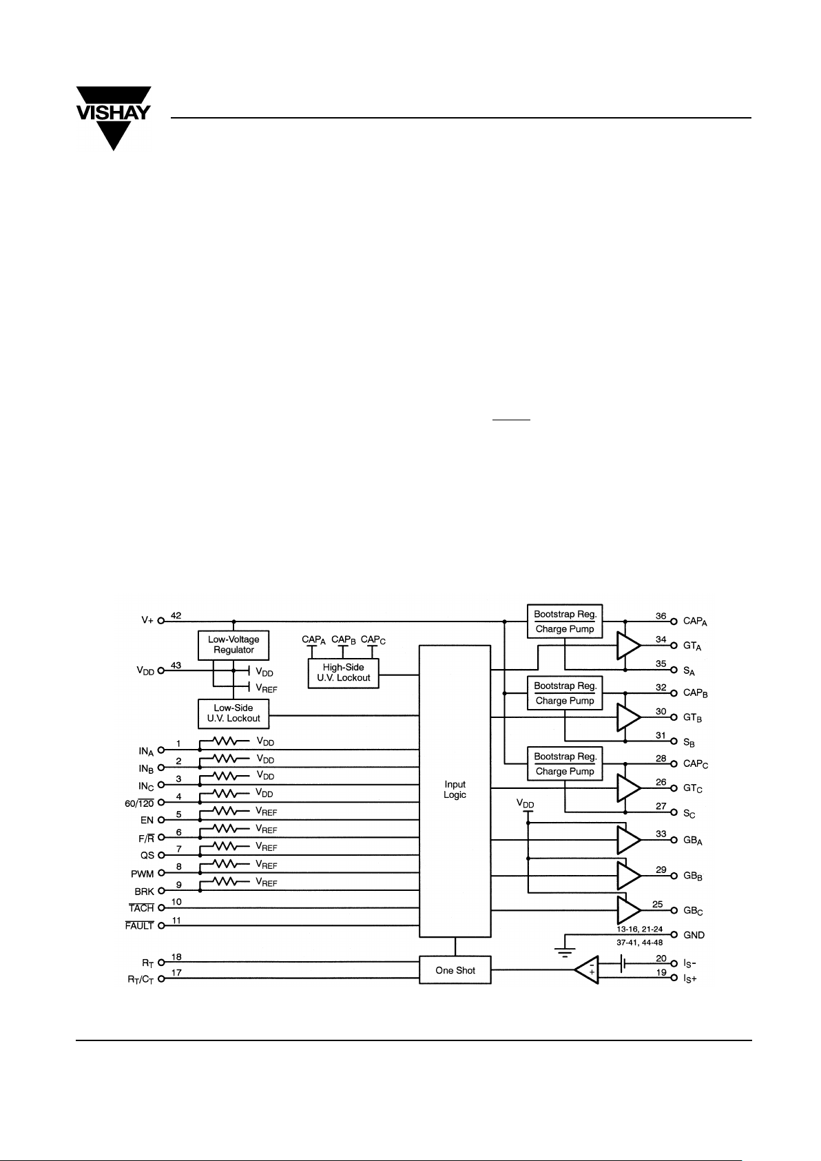
The Si9979 i s a monol ithic brus hless d c moto r contr oller with
integral high-side drive circuitry. The Si9979 is configured to
allow either 60° or 120° commutation sensor spacing. The
internal low-voltage regulator allows operation over a wide
input voltage range, 20- to 40-V dc.
The Si9979 provides commutation from Hall-effect sensors.
The integral high-side drive, which utilizes combination
bootstrap/charge pump supplies, allows implementation of an
all n-channel MOSFET 3-phase bridge. PWM, direction,
quadrature select, and braking inputs are included for control
along with a tachometer output. Protection features include
cross conduction p rotection, current limiting , and un dervoltag e
lockout. The FAULT
output indicates when undervol tag e, over
current, disable, or invalid sensor shutdown has occurred.
The Si9979 is specified to operate over the commercial
temperature range of 0 to 70°C (C suffix), and the industrial
temperature range of -40 to 85°C (D suffix).
FUNCTIONAL BLOCK DIAGRAM
• Hall-Effect Commutation
é 60° or 120° Sensor Spacing
é Integral High-Side Drive for all
N-Channel MOSFET Bridges
é PWM Input
é Quadrature Selection
é Tachometer Output
é Reversible
é Braking
é Output Enable Control
é Cross Conduction Protection
é Current Limiting
é Undervoltage Lockout
é Internal Pull-Up Resistors
Si9979
Si9979
Vishay Siliconix
S-60752-Rev. D, 05-Apr-99 FaxBack 408-970-5600, request 70012
2 www.siliconix.com
ABSOLUTE MAXIMUM RATINGS
Voltage on Pin 42 . . . . . . . . . . . . . . . . . . . . . . . . . . . . . . . . . . . . .50 V
Voltage on Pins 1-4, 10, 11 . . . . . . . . . . . . . . . .-0.3 V to V
DD
+ 0.3 V
Voltage on Pins 5-9 . . . . . . . . . . . . . . . . . . . . . . . . . . . -0.3 V to 5.5 V
Voltage on Pins 26, 28, 30, 32, 34, 36. . . . . . . . . . . . . . . . . . . . .60 V
Voltage on Pins 27, 31, 35. . . . . . . . . . . . . . . . . . . . . . . . . . -2 to 50 V
Operating Temperature
C Suffix. . . . . . . . . . . . . . . . . . . . . . . . . . . . . . . . . . . . . . 0 to 70°C
D Suffix. . . . . . . . . . . . . . . . . . . . . . . . . . . . . . . . . . . . . -40 to 85°C
Storage Temperature. . . . . . . . . . . . . . . . . . . . . . . . . . . .-65 to 150°C
Junction Temperature (T
J
). . . . . . . . . . . . . . . . . . . . . . . . . . . . .150°C
Power Dissipation (P
D
)
C Suffix. . . . . . . . . . . . . . . . . . . . . . . . . . . . . . . . . . . . . . . . 0.70 W
D Suffix. . . . . . . . . . . . . . . . . . . . . . . . . . . . . . . . . . . . . . . . 0.55 W
RECOMMENDED OPERATING RANGE
V+. . . . . . . . . . . . . . . . . . . . . . . . . . . . . . . . . . . . . . . . . +20 to 40 V
DCRT
. . . . . . . . . . . . . . . . . . . . . . . . . . . . . . . . . . . . . . . . . . . . .10 kΩ Min
SPECIFICATIONS
Parameter Symbol
Test Conditi ons
Unless Otherwise Specified
V+ = 20 to 40 V, IDD = 0 mA
Limits
-40°C to 85°C
UnitsMin
a
Typ
b
Max
a
Power
Supply Voltage Range V+ 20 40
V
Logic Voltage V
DD
-20 mA ≤ IDD ≤ 0 mA 14.5 16 17.5
Supply Current I+ 4.5
mA
Logic Current I
DD
-20
Internal Reference
c
V
REF
4.2 V
Commutation Inputs (INA, INB, INC, 60/120)
High-State V
IH
4.0
V
Low-State V
IL
1.0
High-State Input Current I
IH
VIH = V
DD
10
µ
A
Low-State Input Current I
IL
VIL = 0 V -50
Logic Inputs (F/R, EN, QS, PWM, BRK)
High-State V
IH
2.0
V
Low-State V
IL
0.8
High-State Input Current I
IH
VIH = 5.5 V 10
µ
A
Low-State Input Current I
IL
VIL = 0 V -125
Outputs
Low-Side Gate Drive, High State V
GBH
14 16 17.5
V
Low-Side Gate Drive, Low State V
GBL
0.1
High-Side Gate Drive, High State V
GTH
TA = 0 to 70°C
C Suffix
16 18
T
A
= -40 to 85°C
D Suffix
16 20
High-Side Gate Drive, Low State V
GTL
0.1
Capacitor Voltage
d
V
CAP
V+ = 40 V 55
Low-Side Switching, Rise Time t
rL
Risetime = 1 to 10 V
Falltime = 10 to 1 V
C
L
= 600 pF
70
ns
Low-Side Switching, Fall Time t
fL
25
High-Side Switching, Rise Time t
rH
100
High-Side Switching, Fall Time t
fH
40
Break-Before-Make Time
t
BLH
100
t
BHL
300
TACH
Output/FAULT Output V
OL
IOL = 1.0 mA 0.15 0.4 V
TACH
Output Pulsewidth t
T
300 600 ns
Si9979
Vishay Siliconix
FaxBack 408-970-5600, request 70012 S-60752-Rev. D, 05-Apr-99
www.siliconix.com 3
Notes
a. The algebraic convention whereby the most negative value is a minimum and the most positive a maximum.
b. Typical values are for DESIGN AID ONLY, not guaranteed nor subject to production testing.
c. The reference voltage is not available for external use.
d. V
CAP
= (V+) + (VDD)
Notes: L. Any valid sensor combination X. Don’t care
Protection
Low-Side Undervoltage Lockout UVLL 12.2
VLow-Side Hysteresis V
H
0.8
High-Side Undervoltage Lockout UVLH S
A, B, C
= 0 V VDD - 3.3
Current Limit
Comparator Input Bias Current I
IB
-5
µ
A
Comparator Threshold Voltage V
TH
TA = 0 to 70°C C Suffix 90 100 110
mV
T
A
= -40 to 85°C D Suffix 85 100 125
Common Mode Voltage V
CM
01V
One Shot Pulse Width t
p
RT = 10 k, CT = 0.001 µF81012
µ
s
R
T
= 10 k, CT = 0.01 µF 80 100 120
SPECIFICATIONS
Parameter Symbol
Test Conditions
Unless Otherwise Specified
V+ = 20 to 40 V, IDD = 0 mA
Limits
-40°C to 85°C
UnitsMin
a
Typ
b
Max
a
COMMUTATION TRUTH TABLE
Inputs Outputs
Conditions
Sensors
(60°Spacing)
Sensors
(60°Spacing)
EN F/R
BRK IS+
Top Drive Bottom Drive
FAULTINAINBINCINAINBIN
C
GTAGTBGTCGBAGBBGB
C
00010111 0 0100010 1
10010011 0 0100001 1
11011011 0 0010001 1
11101011 0 0010100 1
01101111 0 0001100 1
00100111 0 0001010 1
00010110 0 0010100 1
10010010 0 0001100 1
11011010 0 0001010 1
11101010 0 0100010 1
01101110 0 0100001 1
00100110 0 0010001 1
XXXXXX0X 0 X 000000 0 Disable
XXXXXX0X 1 X 000111 0Power Down
LLLLLL1X 1 0 000111 1 Brake
LLLLLL1X 1 1 000111 0Over I in BRK
LLLLLL1X 0 1 000000 0 Over I
1011111X 0 X000000 0
1011111X 1 X000111 0
0100001X 0 X000000 0
0100001X 1 X000111 0

Si9979
Vishay Siliconix
S-60752-Rev. D, 05-Apr-99 FaxBack 408-970-5600, request 70012
4 www.siliconix.com
PIN CONFIGURATION
PIN DESCRIPTION
Pins 1-3: INA, INB, IN
C
INA, INB, and INC are the commutation sens or inputs, and are
intended to be driven by open collector Hall effect switches.
These inputs have internal pull up resistors tied to VDD, which
eliminates the need for external pull up resistors.
Pin 4: 60/120
The 60/120 input allows th e use of th e Si9979 wit h either a 6 0°
or 120° commutation sensor spacing. An internal pull up
resistor, w hic h is t ied t o V
DD
, sets the default condition to 60°
spacing. 120° spacing is selected by pulling this input to
ground.
Pin 5: EN (Enable)
A logic “1” on this input allows commutation of the motor. This
is the default condi tion as this pin is pu lled up internal ly. Whe n
this pin is pulled to ground, al l gate drive o utputs are turne d off.
Pin 6: F/R
(Forward/Reverse)
A logic “1” on this input selects commutation for motor rota tion
in the “forward” direction. This is the default condition as this
pin is pulled up internally. Whe n this pin is pulled to ground , the
commutation sensor logic levels are inverted internally,
causing reverse rotation.
Pin 7: QS (Quadrature Select)
This input determines whether the bottom MOSFETs or both
bottom and top MOSFETs switch in response to the PWM
signal. A logic “1” on this input enables only the bottom
MOSFETs. This is the default condition as this pin is pulled up
internally. When this pin is pulled to ground, both the bottom
and top MOSFETs are enabled.
Pin 8: PWM
An open collector (drain) or TTL com patible signal is appli ed to
this input to control the moto r spee d. The QS in put de termin es
which MOSFETs are swi tched in resp onse t o the PWM sign al.
If no PWM signal is being used, this input is left open. It is
pulled up internally, which allows the MOSFETs to follow the
commutation sequence.
Pin 9: BRK
With this input at l ogic “1”, the top MOSFETs ar e turned off a nd
the bottom MOSFETs are turned on, shorting the motor
windings together. This provides a braking torque which is
dependent on the motor spee d. This is th e default con dition as
this pin is pulled up internally. When this pin is pulled to
ground, the MOSFETs are allowed to follow the commutation
sequence.

Si9979
Vishay Siliconix
FaxBack 408-970-5600, request 70012 S-60752-Rev. D, 05-Apr-99
www.siliconix.com 5
Pin 10: TACH
This output provides a mi nimum 300-na nosecond ou tput pulse
for every commutation sens or trans ition, yield ing a 6 pulse per
electrical revolution tachometer signal. This output is open
drain.
Pin 11: FAULT
The FAULT output switches low to indicate that at least one of
the following conditions exists, controller disable (EN
),
undervoltage lockout, invalid commutation sensor code
shutdown, or overcu rrent shutdown. This output is open drain.
Pin 17: R
T/CT
The junction of the current limit one shot timing resistor and
capacitor is connec ted to this pin. This one-shot is trigge red by
the current limit comparator when an overcurrent condition
exists. This action turns off all the gate drives for the period
defined by R
T
and C
T
, thus stopping the flow of current.
Pin 18: R
T
One side of the current limit one shot timing resistor is
connected to this pin.
Pin 19: I
S
+
This is the sensing input of the current limit comparator and
should be connected to the positive side of the current sense
resistor. When the voltage across the current sense resistor
exceeds 100 mV, the comparator switches and triggers the
current limit one-sh ot. The one-sho t turns off all th e gate drives
for the period defined by R
T
and CT, thus stopping the flow of
current. If the overcurrent condition remains after the
shutdown period, the gate drives will be held off until the
overcurrent condition no longer exi sts.
Pin 20: I
S
-
This pin is the ground reference for the current limit
comparator. It shou ld b e c onnected directly to the gro und si de
of the current sense resistor to enhance noise immunity.
Pins 12-16, 21-24, 37-41, 44-48: GND
These pins are the return path for bo th the logic and ga te drive
circuits. Also, they serve to conduct heat out of the package,
into the circuit board.
Pin 25: GB
C
This is the gate drive output for the bottom MOSFET in
Phase C.
Pin 26: GT
C
This is the gate drive output for the top MOSFET in Phase C.
Pin 27: S
C
This pin is negative supply of the high-side drive circuitry. As
such, it is the c onn ec tio n f or t he neg ative side of the boots tra p
capacitor, the top MOSFET Source, the bottom MOSFET
Drain, and t he Phase C output.
Pin 28: CAP
C
This pin is the positive supply of the high-side circuitry. The
bootstrap capacito r for Phase C is c onnec ted betw een thi s pin
and SC.
Pin 29: GB
B
This is the gate drive output for the bottom MOSFET in
Phase B.
Pin 30: GT
B
This is the gate drive output for the top MOSFET in Phase B.
Pin 31: S
B
This pin is negative supply of the high-side drive circuitry. As
such, it is the conne ction for the ne gative s ide of the boots trap
Pin 34: GT
A
This is the gate drive output for the top MOSFET in Phase A.
Pin 35: S
A
This pin is negative supply of the high-side drive circuitry. As
such, it is the c onn ec tio n f or t he neg ative side of the boots tra p
capacitor, the top MOSFET Source, the bottom MOSFET
Drain, and t he Phase A output.
Pin 36: CAP
A
This pin is the positive supply of the high-side circuitry. The
bootstrap capacitor for Ph as e A i s con nec te d between this pin
and SA.
Pin 42: V+
The supply voltage for the Si9979 is connected between this
pin and ground. The internal logic and high-side supply
voltages are derived from V+.
Pin 43: V
DD
VDD is the internal l ogi c and ga te drive voltage. It is n ecessary
to connect a capacitor between this pin and ground to insure
that the current surges seen at the turn on of the bottom
MOSFETs does not trip the undervoltage lockout circuitry.

Si9979
Vishay Siliconix
S-60752-Rev. D, 05-Apr-99 FaxBack 408-970-5600, request 70012
6 www.siliconix.com
APPLICATIONS
FIGURE 1. Three-Phase Brushless DC Motor Controller
FIGURE 2. Single H-Bridge Controller

Si9979
Vishay Siliconix
FaxBack 408-970-5600, request 70012 S-60752-Rev. D, 05-Apr-99
www.siliconix.com 7
FIGURE 3. Three-Phase AC Motor Controller
FIGURE 4. External V
DD
Regulator
 Loading...