

Page 1

12-V VCM/Spindle Motor Driver for Large Capacity HDD
FEATURES
• 12-V Motor Supply
• Blocking Schottky Diode Replaced by External Synchronous Rectifier
• Spindle Motor Driver Features:
– External LITTLE FOOT® Drivers for High Current/Power Application
– Constant Off-Time PWM Current Drive Mini mizin g Powe r Diss ip ati on
– Sensorless Motor Commutation Immune to PWM Noise
– Externally Controlled Start-Up/Run Function
– Low-Jitter Commutation Output for External Speed Control
– Level Shifting Buffer Amplifier for PWM DAC
– Adjustable Output Slew Rate Control
– Unique Commutation Driver Minimizing Audible Noise
– Programmable Phase Advance for High Speed Motor
– Speed Triggered Motor Brake for Enhanced Reliability
• Voice Coil Motor Driver Features:
– External LITTLE FOOT Drivers for High Current/Power Application
– Low Crossover Distortion in Linear Mode (Class AB)
– Selectable Constant Frequency PWM or Linear Operation
– Programmable Retract Voltage Clamp
– Level Shifting Buffer Amplifier for PWM DAC
– Direct VCM Retract Control Input
– Current Sense Output for Enhanced Servo Control
– Fixed PWM Output Slew Rate Limit
• System Manager Features:
– Power-On Reset Generator
– Adjustable System Voltage Monitor
– 2.3/5.0-V±5%, 150 ppm/°C Reference Output for External PWM DAC
– Programmable Timer for Head Retract and Spindle Brake Delay
– Built-In Test Ability
• 3-Wire Synchronous Serial Data Interface
• Internal Registe rs and Ad dress Dec oding w ith Full Readback Capabi lity
Si9993CS
Vishay Siliconix
Si9993
DESCRIPTION
The Si9993CS consists of a 3-phase brushless dc motor
(spindle) PWM controll er an d a li nea r/PWM transconductance
stage suitable for driving a voice coil motor (head actuator). T o
meet the power handling capability required for a high
capacity hard disk drive, both drivers utilize external LITTLE
FOOT half-bridges (Siliconix Si9942 recommended). A
separate LITTLE FOOT PMOS switch (Si9430) is used as a
FaxBack 408-970-5600, request 70653 S-60752–Rev. A, 05-Apr-99
www.siliconix.com 1
synchronous r ectifier in place of the usual Scho ttky blocking
diode.
Si9993CS is manufactured in a junction-isolated BiC/DMOS
process (JIBCD15) and is available in a 64-pin SQFP
package, specified to operate over the commercial (0°C to
70°C) temperature range.
Page 2
Si9993CS
Vishay Siliconix
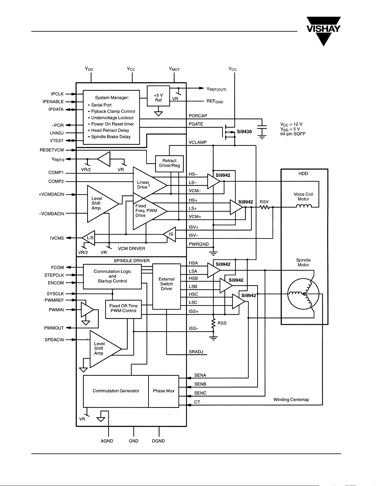
FUNCTIONAL BLOCK DIAGRAM
S-60752–Rev. A, 05-Apr-99 FaxBack 408-970-5600, request 70653
2 www.siliconix.com
Page 3
Si9993CS
Vishay Siliconix
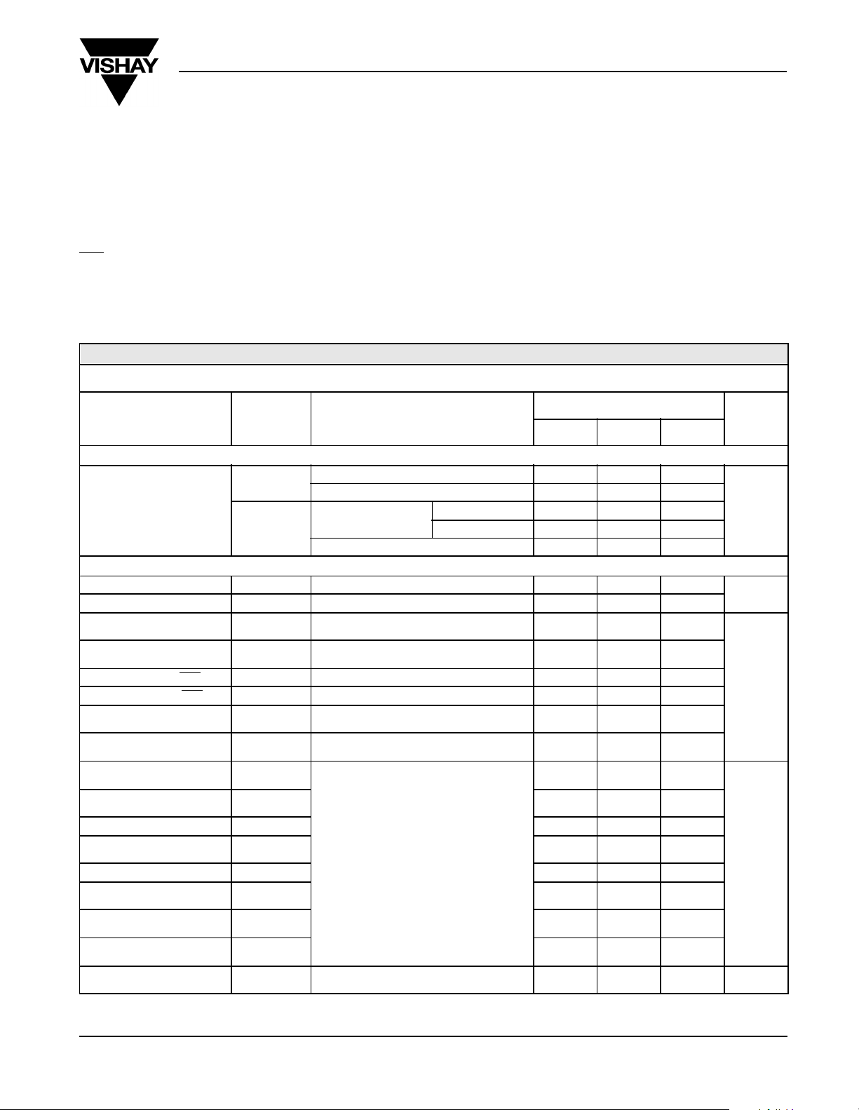
ABSOLUTE MAXIMUM RATINGS (TA = 25°C)*
Voltage Referenced to GND Pin
Supply Range. . . . . . . . . . . . . . . . . . . . . . . . . . . . . . . .-0.3 to 7 V
V
DD
Supply Range. . . . . . . . . . . . . . . . . . . . . . . . . .> (VCC - 0.3 V
V
CLAMP
V
CC
and > (V
, V
Supply Range . . . . . . . . . . . . . . . . . . . . . . . . .-0.3 to 14 V
MOT
- 0.3 V) to 14 V
DD
AGND, DGND, PWRGND to GND. . . . . . . . . . . . . . . . . . -0.3 to 0.3 V
SENA, SENB, SENC, CT, VCM+, VCM-Pin . . . . .-1.0 to V
, FCOM, STEPCLK, ENCOM , SY SCLK, PWMIN,
POR
+ 1.0 V
CC
PWMOUT, RESETVCM, IPCLK, IPDATA
and IPENABLE pins . . . . . . . . . . . . . . . . . . . . . . .-0.3 to V
* Exposure to Absolute Maximum rating conditions for extended periods may affect device reliability. Stresses above Absolute Maximum rating may cause
permanent dama ge. Functional op eration at conditi ons other than th e operating conditio ns specified is not i mplied. Only on e Absolute Maximum rating should be
applied at any one time. Device mounted on one-inch square FR4 Board.
+ 0.3 V
DD
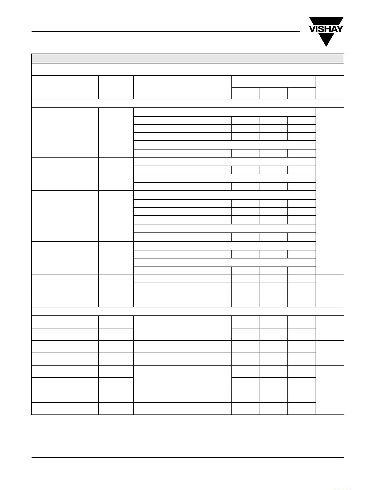
SPECIFICATIONS
Operating Conditions:
VCC = V
R
SRADJ
Parameter Symbol Specific Test Conditions
Power Suppl y
Supply Current
I
CC
Control Logic
Low Input Current I
High Input Current I
Low Input Voltage
(All Digital Inputs)
High Input Voltage
(All Digital Inputs)
Low Output Voltage (POR
High Output Voltage (POR
Low Output Voltage
(FCOM, PWMOU T )
High Output Voltage
(FCOM, PWMOU T )
IPDATA Setup Time to Rising
IPCLK Edge
Rising IPCLK Edge to IPDATA
Hold Time
IPDATA Clock Cycle Time t
IPDATA Hold for IPDATA Driver
Turnaround
IPCLK High and Low Time t
IPDATA Propagation Delay
WRT IPCLK Falling Edge
IPENABLE Setup Time WRT
IPCLK Rising Edge
IPENABLE Hold Time WRT
IPCLK Rising Edge
WRT IPCLK Falling Edge to
Data Tri-State
)V
)V
= 12 V ±10%, VDD = 5 V ±10%, V
MOT
= 20 kΩ ±1%, Si9942-Si9430 LITTLE FOOT Driver, F
I
DD
+ I
I
CLAMP
IL
IH
V
V
OL
OH
V
OL
V
OH
t
t
t
t
t
t
t
MOT
IL
IH
1
2
3
4
5
6
7
8
9
+
Normal Operation, Serial Port Idle 0.2 1.2
D7D6(REG0/5) = 00, All Clocks Disabled 0.02 0.1
Normal Operation
No Load at V
D7D6(REG0/5) = 00, All Clocks Disabled 4 6
REF(OUT)
VIN = V
I
OUT
I
OUT
I
OUT
I
OUT
See Timing Diagram, Figures 1 and 2.
See Timing Diagram, Figures 1 and 2. 10 ns
All Other Pins . . . . . . . . . . . . . . . . . . . . . . . . . . . . -0.3 to V
Maximum Current (All Input Pins). . . . . . . . . . . . . . . . . . . . . .±20 mA
Storage Temperatur e (T
Operating Temperature (T
Junction Temperature (T
). . . . . . . . . . . . . . . . . . . . . . . -65 to 150°C
stg
) . . . . . . . . . . . . . . . . . . . . . . . . .0 to 70°C
A
). . . . . . . . . . . . . . . . . . . . . . . . . . . . . 150°C
J
Power Dissipation . . . . . . . . . . . . . . . . . . . . . . . . . . . . . . . . . . . . . 2 W
Thermal Impedance (
REF(IN)
= V
, RSS = RSV = 0.2 Ω ±1%,
REF(OUT)
SYSCLK
). . . . . . . . . . . . . . . . . . . . . . . . . . 6.25°C/W
Θ
JA
= 5 MHz, TA = 0 to 70°C
Limits
a
With VCM Load 40 65
Without VCM Load 25 40
VIN = 0 V -1
DD
2.0
= 4 mA 0.4
= -4 mA 4.1
= 2 mA 0.4
= -2 mA 4.1
15
15
100
70
45
100
20
Typ
b
Max
1
0.8
100
+ 0.3 V
CC
a
UnitMin
mA
µA
V
ns
FaxBack 408-970-5600, request 70653 S-60752–Rev. A, 05-Apr-99
www.siliconix.com 3
Page 4
Si9993CS
Vishay Siliconix
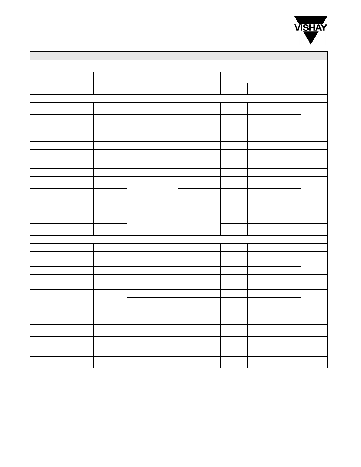
SPECIFICATIONS
Operating Conditions:
VCC = V
R
SRADJ
Parameter Symbol Specific Test Conditions
System Manager
VDD Undervoltage Detection
Threshold (High-to-Low)
VDD Hysteresis 0.05
VCC Undervoltage Detection
Threshold (High-to-Low)
VCC Hysteresis 0.2
POR Time-out t
Delay Time from PWR Failure
to POR Active
POR Charging Current I
POR Comparator Hysteresis 1.0 V
Adjustable Internal Spindle
Brake Delay Time
Internal VCM Retract Delay
Time
Leakage I
V
TEST
5-V Reference Initial P ower-On
T olerance
5-V Reference Drift from Initial
Power-On To lerance
VCM Driver
Transconductance G
Output Offset Current I
DAC Reference Output V
VCMDACIN Input Range +VCMDACIN or -VCMDACIN to GND 0.1 5.0
VCMDACIN Input Bias Current I
Feedback Resistance R
3-dB Bandwidth
CMRR of Current Sense
Amplifier
Head Retract Voltage Clamp I
Short Circuit Head Retract
Current
Current Sense Amplifier Zero
Output Voltage
Current Sense Amplifier
Output Gain Ratio
V(IVCMS)
V(IVCMS)/
= 12 V ±10%, VDD = 5 V ±10%, V
MOT
= 20 kΩ ±1%, Si9942-Si9430 LITTLE FOOT Driver, F
REF(IN)
= V
, RSS = RSV = 0.2 Ω ±1%,
REF(OUT)
= 5 MHz, TA = 0 to 70°C
SYSCLK
Limits
a
Unconnected 4.500 4.625 4.750
UV
ADJ
8.5 9.25 10.0
POR
t
POR
POR
t
spindly
t
vcmdly
VTEST
V
REF
V
∆
REF
---------------- -
V
REF
mVCM
OS
REF/2
(L/S) 50 nA
b
FB
V
CLAMP
V
V
REF(IN)
Internal Resistor from IVCMS to COMP1 12 k
PORCAP = 0.5 µF 350 500 650 ms
= 3.0 to 13.2 V
= VCC = 0 V
DD
V
= 3.0 V, VDD = VCC = 0 V
CLAMP
V
TEST
= V
REF(OUT)
= 20 mA to -2 mA
I
OUT
I
= 1 A, D5D4(REG0) = 11 1.52 1.60 1.68 A/V
MOTOR
D3D2(REG1) = 01 192
D5D4(REG1) = 01 8
= 10 V
(Internal Reference)
4.75 5.00 5.25 V
-1.5 1.5 %
D5D4(REG0) = 11 -25 0 25 mA
R
LOAD
= 100 k
Ω
2.09 2.2 2.31
L/S, I/S and Comp Amp 1.0
Class B Power Amp 0.4
CM Input = 0 to V
= 60 mA, D7D6(REG1) = 00 0.32 0.4 0.48 V
MOTOR
CC
120 180 mA
= 0
I
D7D6(REG0) = 00, D7D6(REG5) = 11
D7D6(REG0) = 00, D7D6(REG5) = 11
V(RSV)
MOTOR
I
MOTOR
= 0
2.32 2.5 2.68 V
dc Gain 2.67 V/V
Typ
b
Max
a
0.8 1.0 µS
2µA
1µA
70 dB
UnitMin
V
ms
V
Ω
MHz
S-60752–Rev. A, 05-Apr-99 FaxBack 408-970-5600, request 70653
4 www.siliconix.com
Page 5
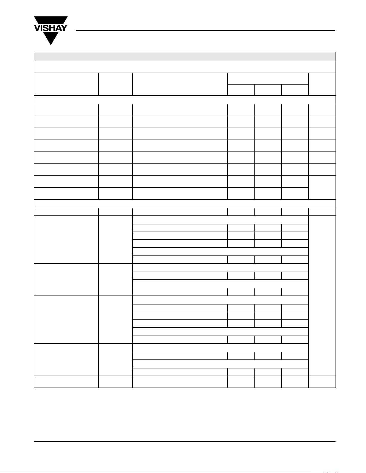
SPECIFICATIONS
Operating Conditions:
VCC = V
R
SRADJ
Parameter Symbol Specific Test Conditions
Spindle Motor Driver
Transconductance
Spindle Driver Input Offset
Voltage
Current Sense Comparator
Input Bias Current
PWM Constant Off-Time
Stability
Spindle Driver Input Bias
Current
BEMF Detect Input Offset
Voltage
BEMF Detect CM Input Range 2.5
Power-Down Spindle Motor
Break Threshold
(Start-Up)
V
PWM Pre-Driver for LITTLE FOOT® (Spindle Motor)
SRADJ Voltage V
HSA/B/C Output
High Current (OFF)
HSA/B/C Output
Low Current (ON)
LSA/B/C Output
Low Current (OFF)
LSA/B/C Output
High Current (ON)
SENA/B/D and VCM ± Clamp
Diode Voltage
= 12 V ±10%, VDD = 5 V ±10%, V
MOT
= 20 kΩ ±1%, Si9942-Si9430 LITTLE FOOT Driver, F
G
MSPIN
(SPDACIN)
(C/S) 2 µA
I
B
= 1 A, D5D4(REG5) = 11 1.44 1.60 1.76 A/V
I
MOTOR
I
= 0 A, D5D4(REG5) = 11 40 mV
MOTOR
REF(IN)
= V
, RSS = RSV = 0.2 Ω ±1%,
REF(OUT)
= 5 MHz, TA = 0 to 70°C
SYSCLK
D3/D2(REG5) = 01 3.2 3.4 µs
(L/S) 50 nA
I
B
-20 20 mV
Measured at V
SRADJ
, D1D0(REG1) = 11 2.4 3.0 3.6
CLAMP
I
= -50 µA 1.0 V
SRADJ
D2/D1(REF4) = 11
V
= V
OUT
= V
V
(HS)
I
OH
OUT
- 3 V, Slew Controlled Range -1.6
CLAMP
= V
V
OUT
- 0.4 V -1.6
CLAMP
- 10V -24
CLAMP
D2/D1(REF4) = 00
V
OUT
= V
- 3 V -13
CLAMP
D2/D1(REF4) = 11
V
= V
(HS)
I
OL
OUT
D2/D1(REF4) = 00
- 3 V, Slew Controlled Range 1.4
CLAMP
V
= 3 V 19
OUT
D2/D1(REF4) = 11
V
= 0.4 V 1.9
OUT
= 3 V, Slew Controlled Range 1.7
V
(LS)
I
OL
OUT
= 10V 5.0
V
OUT
D2/D1(REF4) = 00
V
= 3 V 13
OUT
D2/D1(REF4) = 11
V
= 3 V, Slew Controlled Range -1.1
(LS)
I
OH
V
CL
OUT
D2/D1(REF4) = 00
V
= 3 V -7
OUT
Measured at IF = 20 mA and IF = -20 mA 0.5 V
Si9993CS
Vishay Siliconix
Limits
a
Typ
b
Max
V
CLAMP
a
2
UnitMin
V
mA
FaxBack 408-970-5600, request 70653 S-60752–Rev. A, 05-Apr-99
www.siliconix.com 5
Page 6
Si9993CS
Vishay Siliconix
SPECIFICATIONS
Operating Conditions:
VCC = V
R
SRADJ
Parameter Symbol Specific Test Conditions
PWM Pre-Driver for LITTLE FOOT (VCM)
HS ± Output High
Current OFF
HS ± Output Low
Current ON
LS ± Output Low
Current OFF
LS ± Output High
Current ON
Upper VCM
Slew Rate Threshold
Lower VCM
Slew Rate Threshold
VCMSR
VCMSR
VCM Linear Pre-Driver for LITTLE FOOT
HS ± Linear
High Output Voltage
HS ± Linear
Low Output Voltage
HS ± Linear
Output High Current
HS ± Linear
Output Low Current
LS ± Linear
High Output Voltage
LS ± Linear
Low Output Voltage
LS ± Linear
Output High Current
LS ± Linear
Output Low Current
Notes
a. The algebraic convention whereby the most negative value is a minimum and the most positive a maximum, is used in this data sheet.
b. Typical values are for DESIGN AID ONLY, not guaranteed or subject to production testing.
= 12 V ±10%, VDD = 5 V ±10%, V
MOT
= 20 kΩ ±1%, Si9942-Si9430 LITTLE FOOT Driver, F
REF(IN)
With Slew Rate Control
V
IOH(HS)
= V
OUT
= V
V
OUT
- 3 V, Slew Controlled Range -1.6
CLAMP
V
OUT
- 0.4 V -1.6
CLAMP
= V
- 10V -24
CLAMP
Without Slew Rate Control
V
OUT
= V
- 3 V -1.4
CLAMP
With Slew Rate Control
IOL(HS)
= V
OUT
Without Slew Rate Control
- 3 V, Slew Controlled Range 1.4
CLAMP
V
= 3 V 3.1
OUT
V
With Slew Rate Control
V
= 0.4 V 1.9
OUT
= 3 V, Slew Controlled Range 1.7
V
IOL(LS)
OUT
V
= 10V 5.0
OUT
Without Slew Rate Control
= 3 V 3.1
V
OUT
With Slew Rate Control
V
= 3 V, Slew Controlled Range -1.1
IOH(LS)
V
OH
V
OL
I
OH
I
OL
V
OH
V
OL
I
OH
I
OL
th+
th-
OUT
Without Slew Rate Control
V
= V
OUT
From Low to High VCC = V
Hysteresis 2.3
From Low to High VCC = V
Hysteresis 1.7
V
= V
OUT
V
V
= V
OUT
V
- 3 V -1.4
CLAMP
I
= 0
OUT
- 3 V -1.4
CLAMP
= 3 V 3.1
OUT
I
= 0
OUT
- 3 V -1.4
CLAMP
= 3 V 3.1
OUT
CLAMP
CLAMP
= V
, RSS = RSV = 0.2 Ω ±1%,
REF(OUT)
= 5 MHz, TA = 0 to 70°C
SYSCLK
a
= 12 V 10.3
= 12 V 1.3
V
V
Limits
Typ
CLAMP
0.8
1.4
CLAMP
1.6
0.7
b
Max
a
-
-
UnitMin
mA
V
V
mA
V
mA
S-60752–Rev. A, 05-Apr-99 FaxBack 408-970-5600, request 70653
6 www.siliconix.com
Page 7
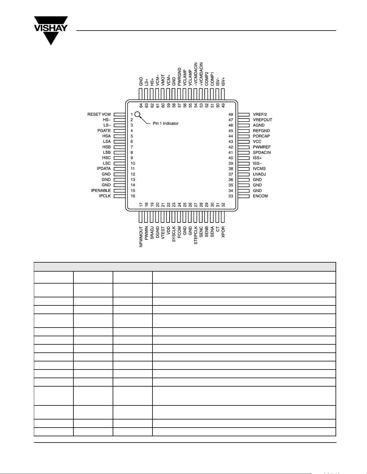
PIN CONFIGURATION
Si9993CS
Vishay Siliconix
PIN DESCRIPTION
Pin No. Name Type Function
1 RESETVCM Digital, Input
2 HS- Analog, Output Connection to gate of negative VCM high-side driver
3 LS- Analog, Output Connection to gate of negative VCM low-side driver
4 PGATE Analog, Output
5 HSA Analog, Output Connection to gate of spindle 0-A high-side driver
6 LSA Analog, Output Connection to gate of spindle 0-A low-side driver
7 HSB Analog, Output Connection to gate of spindle 0-B high-side driver
8 LSB Analog, Output Connection to gate of spindle 0-B low-side driver
9 HSC Analog, Output Connection to gate of spindle 0-C high-side driver
10 LSC Analog, Output Connection to gate of spindle 0-C low-side driver
11 IPDATA Digital, I/O Bi-directional data path for the serial port
12, 13, 14, 25,
26, 34, 35, 36,
58, 64
15 IPENABLE Digital, Input
16 IPCLK Digital, Input Clock input for the serial port
17 PWMOUT Digital, Output Digital output of stand-alone PWM driver
GND Supply Chip substrate ground
Direct RESET to bit D6 of REG0. Force head retract sequence if in normal
operation.
Connection to gate of external PMOSFET used to isolate VCLAMP during
emergency head retract.
Strobe input for data word. System commands are executed at the falling edge of
IPENABLE.
FaxBack 408-970-5600, request 70653 S-60752–Rev. A, 05-Apr-99
www.siliconix.com 7
Page 8
Si9993CS
Vishay Siliconix
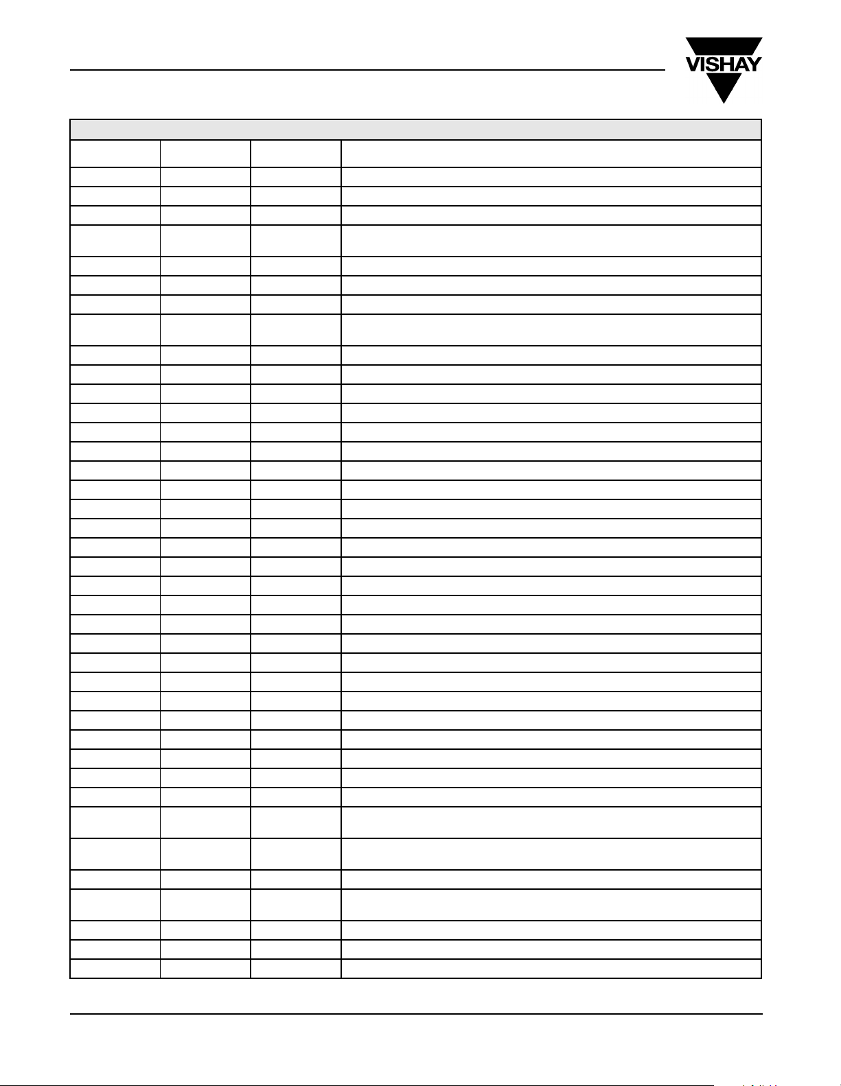
PIN DESCRIPTION
Pin No. Name Type Function
18 PWMIN Digital, Input Digital input of stand-alone PWM driver
19 SRADJ Analog, Input Spindle Output drive slew rate control
20 DGND Supply Digital negative supply
21 VTEST Analog, I/O
22 VDD Supply +5 V digital power supply
23 SYSCLK Digital, Input System clock input (5Mhz) for onboard timers
24 FCOM Digital, Output Commutation clock output for external speed control
27 STEPCLK Digital, Input
28 SENC Analog, Input Input to BEMF-sense circuitry; connect to 0-C
29 SENB Analog, Input Input to BEMF-sense circuitry, connect to 0-B
30 SENA Analog, Input Input to BEMF-sense circuitry, connect to 0-A
31 CT Analog, Output Center Tap
32 POR Digital, Output Power-on-reset pulse for entire drive electronics
33 ENCOM Digital, Input Enable input for onboard commutation clock generator
37 UVADJ Analog, Output External Undervoltage threshold adjust
38 IVCMS Analog, Output VCM current sense output; signal referred to V
39 ISS- Analog, Input Negative input to spindle current sense amplifier
40 ISS+ Analog, Input Positive input to spindle current sense amplifier
41 SPDACIN Analog, Input Spindle Input (from PWM DAC Out)
42 PWMREF Analog I/O Reference supply input for stand-alone PWM driver
43 VCC Supply +12 V analog power supply for the whole chip
44 PORCAP Analog, Output Connect to Power-on-reset timing capacitor
45 REFGND Supply Critical analog ground reference
46 AGND Supply Analog negative supply and ground reference
47 VREF(OUT) Analog, Output Reference supply output for stand-alone PWM DAC and VCM common
48 VREF/2 Analog, Output Reference supply output for external VCM DAC
49 ISV+ Analog, Input Positive input to VCM current sense amplifier
50 ISV- Analog, Input Negative input to VCM current sense amplifier
51 COMP1 Analog, Output Connection for external VCM R/C compensation
52 COMP2 Analog, Input Connection for external VCM R/C compensation
53 +VCMDACIN Analog, Input Positive VCM input (from +VCM DAC Out)
54 -VCMDACIN Analog, Input Negative VCM input (from -VCM DAC Out)
55, 56 VC LAM P Supply
57 PWRGND Supply
59 VCM+ A nalog, I/O Feedback from the positive output of VCM driver
60 VMOT S upply
61 VCM - Analog, I/O Feedback from the negative output of VCM driver
62 HS+ Analog, Output Connection to gate of positive VCM high-side driver
63 LS+ Analog, Output Connection to gate of positive VCM low-side driver
External charge storage node for spindle brake function. Also used as a
manufacturer’s test pin
Clock input for spindle commutation state machine, used during spindle start-up
only
REF/2
+12-V digital power supply for spindle PWM section; also, inductive flyback clamp
and emergency head retract power supply
Ground return referred to external VCM n-channel FETs; used to power VCM class
AB stage.
+12-V power supply referred to external VCM p-channel FETs; used to power VCM
class AB stage.
S-60752–Rev. A, 05-Apr-99 FaxBack 408-970-5600, request 70653
8 www.siliconix.com
Page 9
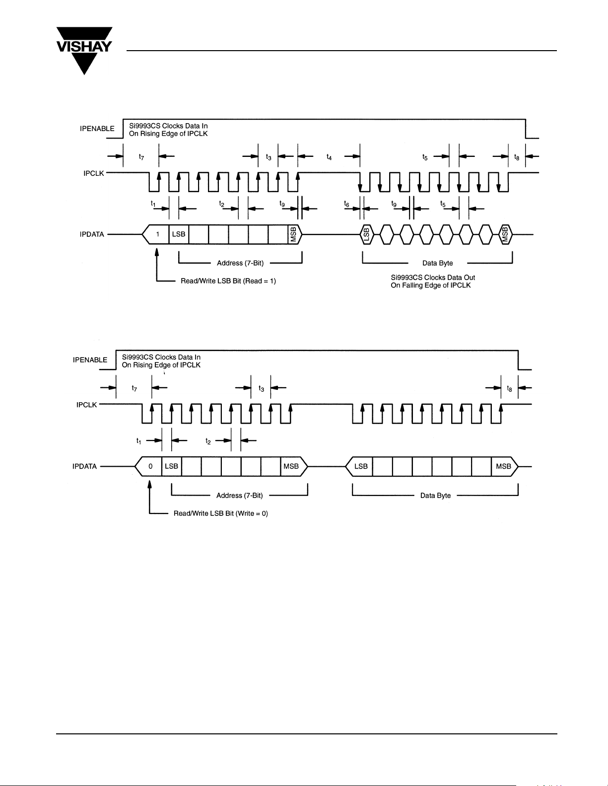
TIMING WAVEFORMS AND TEST CIRCUIT
FIGURE 1. Read Cycle Timing Diagram
Si9993CS
Vishay Siliconix
FIGURE 2. Write Cycle Tim ing Diag ram
FaxBack 408-970-5600, request 70653 S-60752–Rev. A, 05-Apr-99
www.siliconix.com 9
Page 10

Si9993CS
Vishay Siliconix
FUNCTIONAL DESCRIPTION
Voice Coil Motor Driver
The VCM driver provides all necessary control functions, for a
linear transconductance stage, including a motor current
sense amplifier, a loop compensation amplifier and a 3-A
power amplifier featuring two Si9942’s (external) in a full
H-bridge configuration. The output half-bridge operates in the
Class B mode during seeking. The track following mode is
primarily a function of an onboard cla ss AB bipola r driv e r. The
output crossover distortion is kept to a minimum by the
combined BiCMOS driver. Two external components (R3 and
C3) are required to set the bandwidth of the full
transconduc tan ce sta ge. For great er fl exibili ty in inter facing to
the external D/A converter, a DAC reference, an input level
shifting amplifier and gain select are included. To minimize
power dissipation of the power stage during the seek
operation, the VCM driver may also be re-configured (via Bit
D3/2 of REG0, see Table 2) into a constant frequency
Pulse-Width-Modulated (PWM) driver. No additional external
components are required for this useful option. The head
retract circuitry can be acti v ated b y an undervol tage con dition ,
an external command via serial port, or direct control via the
RESETVCM pin. The retract voltage clamp is programmable
from 0.4 to 1.2 V.
External VCM DAC Operation
The VCM driver of the Si9993 CS is desi gned to inte rf ace to an
external DAC with an output range from 0.1 V to 4.5 V and
uses the internal 2.3 V as the mid-point reference (signal
common). Therefore, a differential input of up to ±2.2 V may
be accepted. Depending on the type of DAC chosen, either
(+2.3 V) or V
V
REF/2
reference. The inaccuracy of the mi d-point reference may be
eliminated through calibration by disabling the VCM driver
[D7/D6 (REG0) = 00 or 01] and digitizing the VCM current
sense output (IVCMS). The digitized value is to be stored in
the ASIC or DSP as the VCM current zero scale correction
factor. A differential level shift amplifier has been added
between the internal 12-V current sense amplifier and the
IVCMS pin such that an external ADC operating from a 5-V
power supply may be used directly.
Spindle Motor Driver
The spindle driver powers a three-phase brushless dc motor
in open drive configuration and utilizing a Hall sensor-less
commutation technique. To minimize power stress on the
three Si9942 (external) half-bridges, the driver operates in full
time, constant off-time or variable frequency, PWM current
mode. A proprietar y B EMF sensing t ec hn i que, co ns is t in g of a
filter and a programmable EMF zero crossing comparator and
an intellig ent commutatio n delay generator, is used to der ive
(+5.0 V) can be used as the DAC
REF
the proper commutation zero crossing in the presence of
severe PWM noise. The start-up of the motor is initiated by
the microprocessor through the STEPCLK and ENCOM pins.
This arrangement allows the user to tailor a start-up algorithm
for any given drive. As shown in Table 2, the microprocessor
may strobe the STEPCLK pin to force a new motor state
sequentially. Multiple clocking will allow any unde si red sta t e to
be bypassed. At an empirically determined time, the internal
commutation clock generation loop may be closed by forcing
ENCOM high. For complete interfacing to the
microprocessor’s PWM DAC, a level shifting amplifier,
accepting a wide input range (via D5/D4 or REG5), is also
included on chip. To minimize acoustic or EMI noise, the slew
rate of the output drivers (via HSA/B/C and LSA/B/C) may be
programmed by an external resistor connected through the
SRADJ pin. Additional software slew rate controls are
available through D2/D1 of REG4.
The speed control si gnal from the e x ternal micro or DSP is fed
to the output PWM modulator via an external DAC and the
onboard buffer/level shifter. The interface is designed to work
with either PWM or linear DAC. Should a PWM DAC be
chosen, a stand-alone digital buffer is available to level shift
the 5-V signal from the PWM timer (referred to V
supply independe nt sign al (referred to V
the external RC low pass filter.
Adaptive Commutation Delay Operation
Inside the spindle controller of Si9993CS, the desired
30 electrical degrees (or 90 degrees for a single phase) of
commutation delay is generated by sensing the motor
back-emf zero crossing at the unenergized winding with a
current-controlled transconductance amplifier and charging
an internal capacitor to be programmable threshold with the
output current of the amplifier. The delay time generated is
proportional to the speed of the motor because the charging
current is derived from a motor frequency to current converter.
This proprietary analog timing generator, combined with the
external low-pass filter (three 200-kΩ resistors), provide
excellent immunity to the highly unstable PWM noise. The
resulting motor once -around jitter tim e is co mpar ab le to th at of
a linear drive system. Furthermore, the highly integrated
nature of the design has eliminated all external capacitors,
representing a significant savings in cost and board space.
For maximum flexibility, D2/D1 of REG5 may be used to
program the frequency to current converter filter bandwidth.
For very high performance drive, D7/D2 or REG3 programs
the commutation delay threshold in both negative (phase
advance up to 23.5°) and positive (phase delay up to 7.5°)
directions.
), before it is f ed to
REF
1
DD
) to a
S-60752–Rev. A, 05-Apr-99 FaxBack 408-970-5600, request 70653
10 www.siliconix.com
Page 11
Si9993CS
Vishay Siliconix
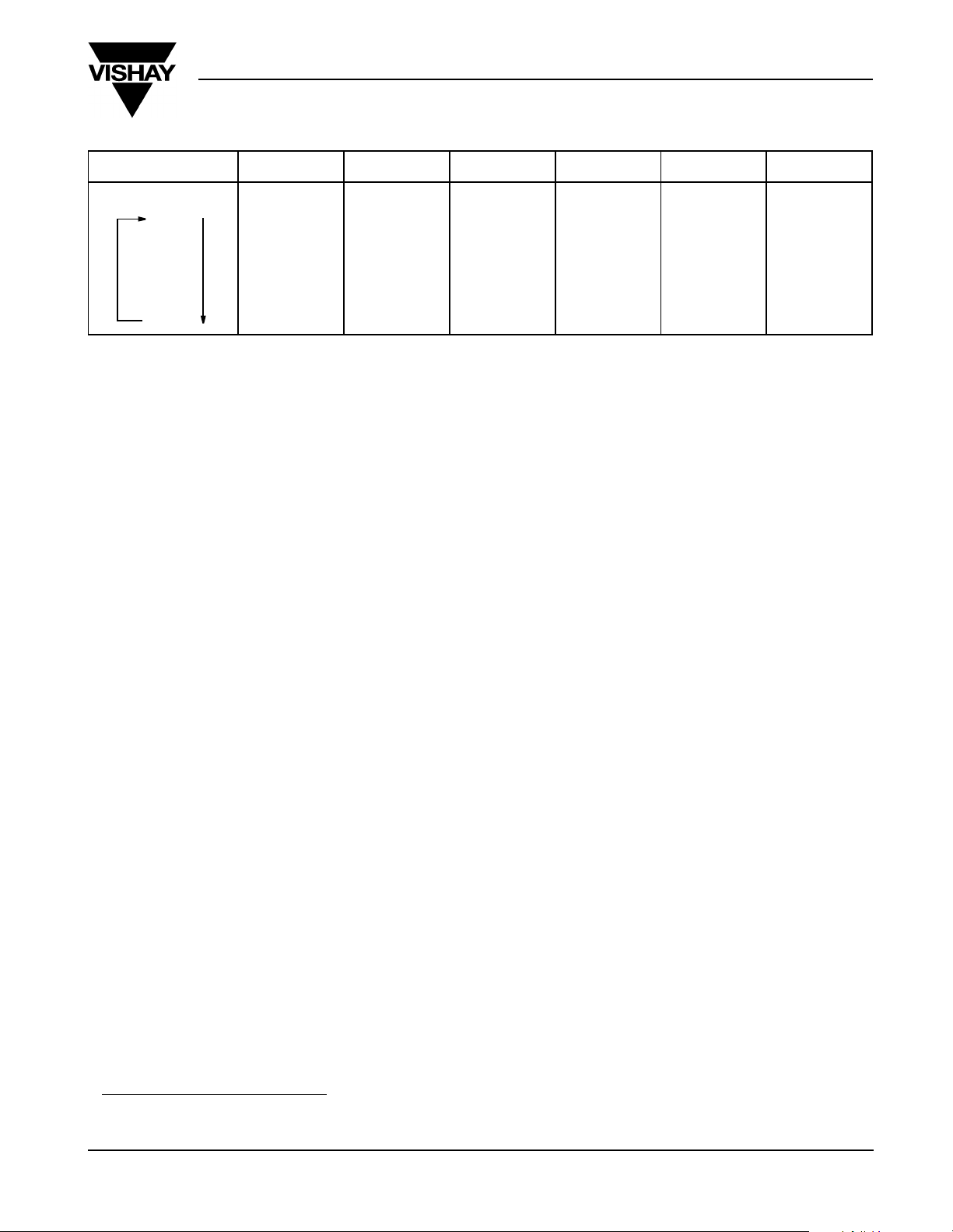
TABLE 1. Spindle Commutation Sequence
Sequencer State HSA LSA HSB LSB HSC LSC
Reset* High Low High Low High Low
1 Low Low High High High Low
2 Low Low High Low High High
3 High Low Low Low High High
4 High High Low Low High Low
5 High High High Low Low Low
6 High Low High High Low Low
*Reset is the state after exiting spindle disable or brake mode.
Quiet Commutation Operation
1
Included on the Si9993CS spindle driver is a unique feedback
circuit which was developed to control the supply current
during the current transfer from one phase of the winding to
another . At the proper time of co mmutation, the ra mp in g d o w n
of the previous phase is regulated to match with the ramping
up of the next phase, which is fully on initially, until all current
has been transferred to the next phase. This not only reduced
the constraint on power supply requirements but also
eliminated annoying high frequency audible noises generated
from second and third harmonics of the commutation
frequency. The “quiet commutation” operation is a function of
PWM off-time and slew rate control. D7/D4 of REG4 may be
used to optimize the circuit performance accordingly.
System Manager
The system manager includes power supply monitor,
power-on reset timer, individual motor on/off control, system
reference generator and a variety of digital delay timers
targeted for PWM and head retract functions. An external
5-MHz system clock is used mainly for the spindle motor
PWM timing functions. An onboard RC oscillator is used to
generate the timing necessary for the emergency motor
shutdown sequence. When a tight microprocessor power
supply is specified, a pair of external resistors may be used to
adjust the V
undervoltage lockout value via UVADJ pin.
DD
Finally, an external capacitor is used to set up the 500-ms
power-on reset pulse for the entire drive electronics. All
controls from the microprocessor or DSP are communicated
via a 16-bit serial port.
be used with the Intel 80C196, AMD 186 processors or other
synchronous serial interfaces.
The serial port allows transfer of a R/W mode bit, seven bits of
register address, and eight bits of data. The port is inactive
when the IPENABLE line is low, and IPCLK must be high.
When IPENABLE is high, the port is active and IPDATA is
strobed on the rising edge of IPCLK. The first bit transferred
on the IPDATA line to the Si9993CS is the R/W mode bit. As
shown in Figure 1, a R/W mode bit of ‘1’ indicates that the
data shall be read from the Si9993CS. Otherwise, the data
shall be wr itten to the S i9993CS as shown in Figure 2. The
next seven bits are the register address. After the transfer of
the address, IPCLK must not switch for a minimu m of 70 ns to
allow the IPDATA line to turn around in case of a read
operation. A fter thi s pause, o ne byte of da ta is tra nsferred to
or from the Si9993CS based on the R/W mode bit. Both the
address and the data are tr ansferred with the L SB first and th e
MSB last. IPENABLE must be lowered to deactivate the port
before the next byte can be transferred. Note that Si9993CS’s
six command registers are NOT decoded by unique binary
address. Each register is identified by a specific address bit.
(i.e. an address of 111111 will access all six registers). The
address and function of each command register and the
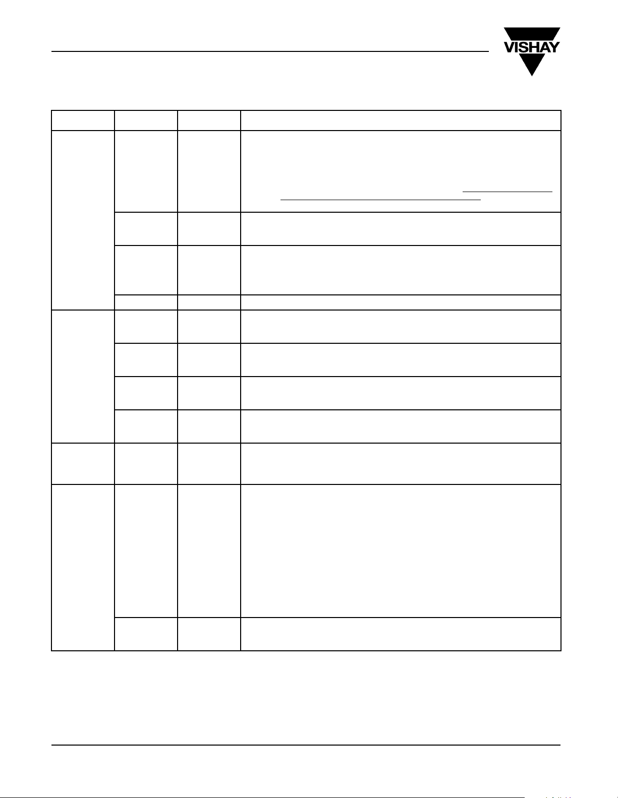
definitio n of each bit wi thin th e regis ter are shown in Table 2.
Note that unused, or open, bits are handled differently.
For write operation, the unused bits may be either 0 or 1.
For read operation, the firs t bit to a ppe ar at the seria l port
is the least significant used bit of the register being read.
Data appearing after the last valid bit should be ignored.
As an example, the data readout sequence for REG1 in
time is D2--D3--D4--D5--D6--D7--X--X.
Serial Port
A 16-bit word, clocked into the serial interface port of the
Si9993CS, provides the means to program basic operating
conditions, control the motor configuration and to force testing
conditions suitable under the production environment. The
serial port is controlled by three signals IPDATA, IPCLK, and
IPENABLE. The IPDATA signal is the bidirectional data line,
the IPCLK si g na l is us e d a s t h e cl ock to va li dat e th e da ta an d
IPENABLE enables serial port operation. This serial port can
Emergency Motor Shutdown Sequence
The Si9993CS executes a motor shutdown sequence
whenever a valid low supply condition is detected (i.e. POR
going from High to Low). Th e circuitr y which cont rols events
within this emergency sequence is powered by spindle
motor’s kinetic energy (BEMF) via the VCLAMP pin. The
critical timing for various events is to be provided by an
onboard RC oscillator and digital counters. The timer’s value
must be progr am me d by the external mic rop roce ss or after the
IC is first powe red up. Note that a simila r “normal” (n ominal
1. Patent Applications Pending
FaxBack 408-970-5600, request 70653 S-60752–Rev. A, 05-Apr-99
www.siliconix.com 11
supply) motor shutdown may be invoked by setting D7/D6 of
Page 12
Si9993CS
Vishay Siliconix
REG5 (Spindle Command) to “00” state. Individual motor
shutdown operation is also possible through the serial port.
Refer to Table 2 for a complete description.
Immediately after detection of the undervoltage condition, all
spindle drivers are turned off while the VCM’s low-side drivers
are turned on to stop the head from any previous movement.
Additionally, all command resistors, except REG1, are reset.
After a time delay, programmed by D5/D4 of REG1, th e VCM’s
retract circuitry is turned on. The spindle drivers remained off.
The head is retracted toward the inside diameter of the disk,
or (VCM+ - VCM-) is positive. The voltage clamp across the
VCM, or the maximum head veloc ity, is limited by the stored
value in D7/D6 of REG1. No programmable current clamp is
available on Si9993CS. The minimum short-circuited VCM
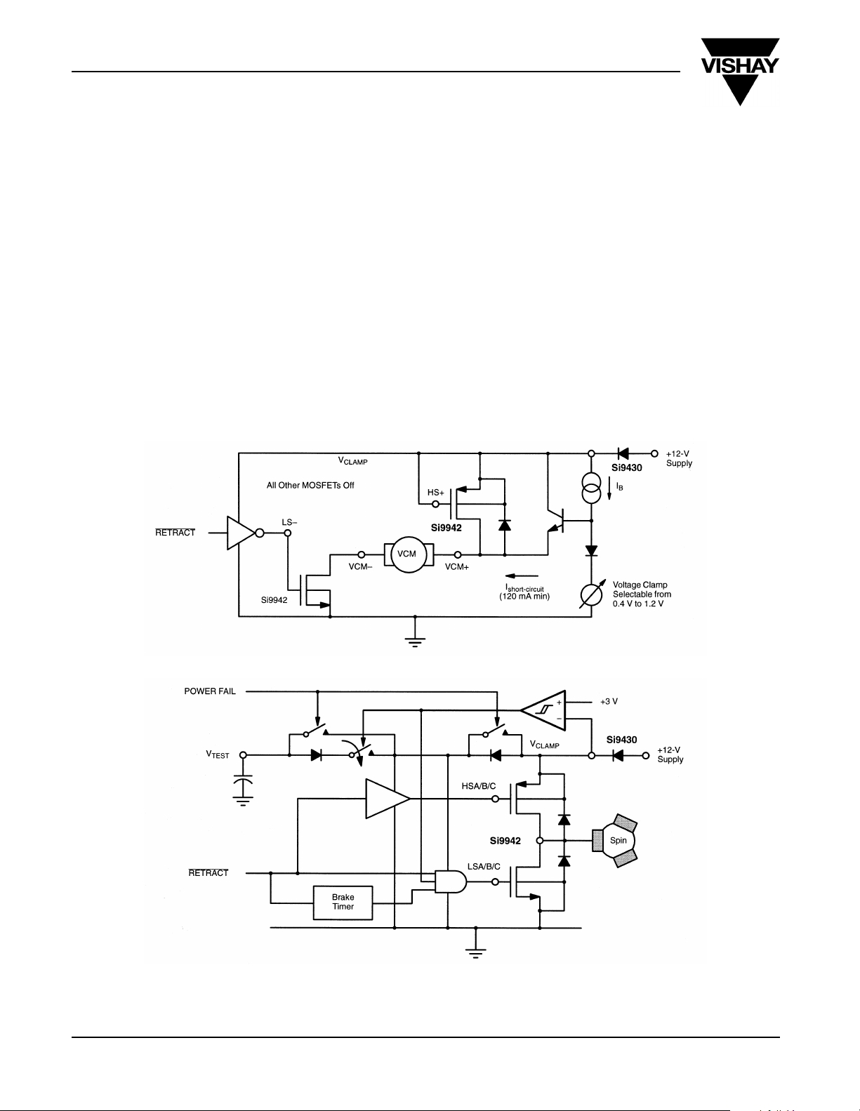
retract current is 120 mA. Refer to Figure 3 for a simplified
schematic.
The head retract time interval, or spindle brake delay time, is
programmed via bit D3/D2 of REG1. After the time-out, the
VCM drivers are turned off (tri-state) and all bits of REG1
except D1/D0 are reset. The state of the spindle motor
low-side drivers are determined by D1/D0) of REG1.
Depending on the motor and the number of disk platters, a
spindle brake at high speed (BEMF voltage of 6 V or higher)
may result in a high amount of energy dissipation in the
LITTLE FOO T drivers. One solutio n to this problem is to us e a
ultra-low r
the dissipation li mit of the Si9942 be exceed ed. In which cas e ,
D1/D0 or RE G1 should be programm ed for immedi ate brake.
A lower cost solution, when feasible, is to allow the motor to
spin down to a lower rpm before the low-side drivers are
turned on to brake the motor. In such case, the motor speed
threshold, which is sensed by measuring the motor BEMF via
V
(Figure 4 shows a 3-V threshold being selected.) Also, as
shown in Figure4, once the spindle brake is on, an external
pre-charged capacitor connected to the V
switched on to maintain the gate drive to the LITTLE FOOT
drivers, even if V
voltage, is programmed using D1/D0 of REG1.
CLAMP
LITTLE FOO T de vi ce , suc h as Si454 4, shou ld
DS(on)
TEST
drops down to zero.
CLAMP
pin will be
FIGURE 3. Simplified Retract Circuit
FIGURE 4. Simplified Spindle Brake Circuit
S-60752–Rev. A, 05-Apr-99 FaxBack 408-970-5600, request 70653
12 www.siliconix.com
Page 13

Si9993CS
Vishay Siliconix
Power-Up Sequence
The POR timer receives the two supply undervoltage
detection outputs and combines them to form one output
called PowerFailure. If PowerFailure is low, the POR output
will remain low. After the power supplies are deemed safe,
Pow erFailure goes high and the timer is turned on whi ch hold s
the POR output low for an additional 500 ms. If PowerFailure
goes back low while the timer is active, the POR output must
remain low and the timer must reset and wait for PowerFailure
to go back high before starting again.
The POR output must drop low within 1 µs from when a pow er
failure is detected. Once the POR output drops low, the timer
must also reset. If the PowerFailure output drops low for less
than 600 ns, then the power failure is ignored and the POR
output remains high and the timer is not reset. The POR
output cannot glitch at anytime. If a power failure is detected,
then the POR output must stay low for a minimum of 350 ms.
A minimum of 1 V of hysteresis exists at the POR comparator
which monitors the timer ramp voltage.
Recommended Parameter Setting Hardware Values and
Register Contents
Spindle
In order to perform some applications testing, some of the
registers should be preloaded and certain hardware values
installed . These are for a fi rst approximation on an average
spindle mo tor and s hou ld b e adj ust ed for th e pa r t icul ar m oto r
and parameters that will be used.
All registers will default to 0 at power-up. The following
register value exceptions should be loaded for an average
motor load.
For start-up:
REG3 D7→D0 = 00000011; 8° Phase Advance, 13-µS PWM
Off-Time
REG4 D7→D0 = 00000000; 1.4-µS On-Time Blanking, 7/8
Off-Time, Slew Rate Off, Q-COM Off
REG5 D2→D0 = 000; 400-ns F/I Sample Time, F/I Speed-Up
On
After reaching speed:
REG3 D7→D0 = 00000001; 8° Phase Advance, 3.4-µS PWM
Off-Time
REG4 D7→D0 = 00000111; 1.4-µS On-Time Blanking, 7/8
Off-Time, Slew Rate On, Q-COM On
REG5 D2→D0 = 110; 40-ns F/I Sample Time, F/I Speed-Up
On
Hardware values:
Resistor from SRADJ to Ground = 20 kΩ for approximately
1-µS Slew Rate
Capacitor from V
to Ground = 1 µF
REF(in)
VCM
The Si9993CS contains a transconductance amplifier to drive
the voice coil motor (VCM). For proper operation, this
amplifier must be compensated specifically for the VCM being
driven. As a first approximation, the torque constant and
inertia of the VCM may be ignored although they will have
some influence on the final results, especially if large.
The VCM transfer function of this simplified case may be
expressed in the s (Laplace) plane as:
1
-----
L
g
v
----------------=
v
R
v
s
------+
L
v
(1)
Where
Rv = VCM resistance in ohms
= VCM inductance in henrys
L
V
s is the Laplace operator
This has a pole at -Rv/Lv. It is desirable to cancel this pole in
the interest of stability. In order to do this, a compensation
amplifier is cascaded with the VCM and its driver. The transfer
function of this amplifier is:
1
s
--------------------+
R
c
-----------------------------------
A
×=
s
H
+
LCL
(2)
Where
RL = compensation amplifier feedback resistor in ohms
= compensation amplifier feedback capacitor in farads
C
L
A = compensation amplifier and driver voltage gain at high frequency
If RL x CL is set equal to Lv/Rv, then the combin ed open loop
transconductance in siemens becomes:
g
A
-------------- -=
to
×
sL
v
(3)
Use these values as the series comb ination from COM P1 to
COMP2. The absolute values should be adjusted for the
desired open loop gain and closed loop bandwidth desired.
This has a single pole at the origin and is therefore stable
when the loop is closed.
FaxBack 408-970-5600, request 70653 S-60752–Rev. A, 05-Apr-99
www.siliconix.com 13
Page 14
Si9993CS
Vishay Siliconix
TABLE 2. Serial Port Definitions (Register Address = A6A5A4A3A2A1A0)
Register Bit No. Name Function
REG0
(xxxxxx1)
VCM Command
REG1
(xxxxx1x)
Powerdown
REG2
(xxxx1xx)
Production
Te st Only
REG3
(xxx1xxx)
Spindle
Controls
D7/D6 VCM Control VCM Enable/Disable Control:
“00” = All VCM amplifiers unbiased except those of current sense. VCM output drivers in
“01” = All VCM amplifiers unbiased except those of current sense. VCM brake always on.
“10” = All VCM amplifiers unbiased except those of current sense. Motor shutdown sequence
“11” = VCM fully enabled for normal operation.
D5/D4 Gmsel(vcm) VCM Transconductance Select (A/V):
“11” = 1.60 “10” = 0.80
“01” = 0.40 “00” = 0.10
D3/D2 VPWM
D1/D0 OPEN OPEN
D7/D6 V
D5/D4 T
D3/D2 T
D1/D0 V
D7 Thru D0 FCOM Pin Configuration Option:
D7 Thru D2 V
retract
vcmdly
spindly
SPBRK
th1
VCM Output State Linear/Constant Frequency PWN Select:
sel
“00” = Output operates as a class AB, linear amplifier
“01” = Output operated in PWM voltage mode at 31.25 kHz
“10” = Output operated in PWM voltage mode at 62.5 kHz
“11” = Output operated in PWM voltage mode at 125 kHz
Head Retract Voltage Limit:
“11” = 0.4 V “10” = 0.7 V
“01” = 1.0 V “00” = 1.2 V
VCM Head Retract Delay Time (from power- down detection or command):
“11” = Zero Delay “10” = 4 ms
“01” = 8 ms “00” = 16 ms
Spindle Brake Delay Time (from power-down detection or command, tvcmdly included):
“11” = Zero Delay “10” = 144 ms
“01” = 192 ms “00” = 384 ms
Spindle Brake Threshold Voltage Select (V
“11” = 3 V “10” = 4 V
“01” = 5 V “00” = Immediate Brake
All other combinations are for testing only, no user programmable parameter is available.
Spindle Commutation Delay Adjust in Sign-Magnitude:
tri-state.
commences with head brake for a period of Tvcmdly, followed by head retract for a
period of Tspindly. The VCM returns to tri-state thereafter. Note that this command has
no effect on the spindle motor operation, or the content of REG5.
“00000000” = FCOM (default)
“10000000” = FCOM/6
The value programmed controls the motor commutation delay, in electrical degree,
from the last BEMF zero crossing via a 6-bit DAC. Each LSB corresponds to ½
electrical degree.
“011111” = 7.5° Delay
:=:
“010000” = 0° Neutral
:=:
“000001” = 7.5° Advance
“000000” = 8° Advance, “100000” = 8° Advance
“100001” = 8.5° Advance
:=:
“110000” = 16° Advance
:=:
“111111” = 23.5° Advance
D1/D0 Tspinpwm Spindle Constant Off-Time (f
“11” = 13 µs “10” = 6.6 µs
“01” = 3.4 µs “00” = 1.8 µs
SYSCLK
CLAMP
= 5 MHz):
Detect):
S-60752–Rev. A, 05-Apr-99 FaxBack 408-970-5600, request 70653
14 www.siliconix.com
Page 15
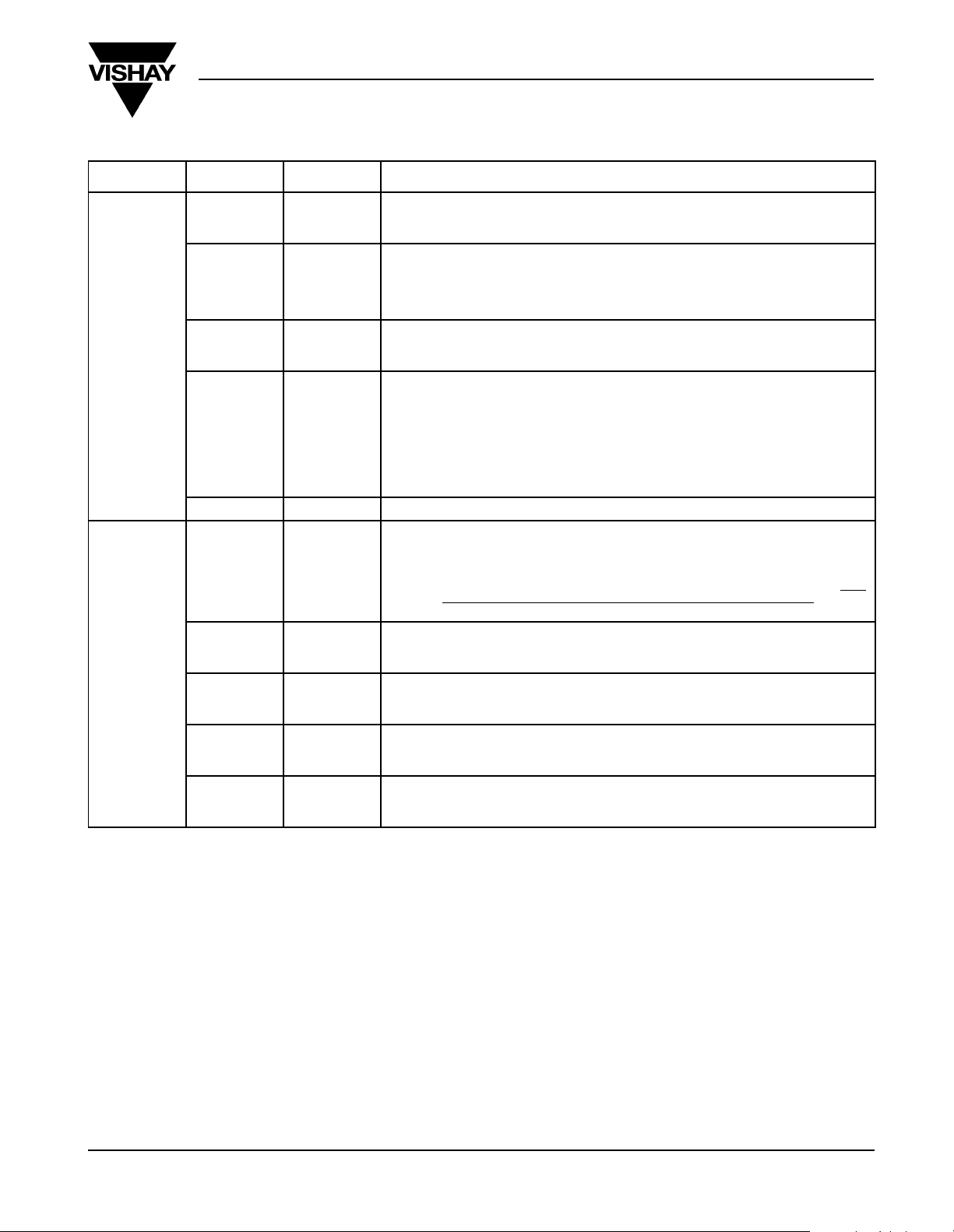
TABLE 2. Serial Port Definitions (Register Address = A6A5A4A3A2A1A0) (Continued)
Register Bit No. Name Function
REG4
(xx1xxxx)
Driver Controls
REG5
(x1xxxxx)
Spindle
Command
D7/D6 Tblank(on) PWM On-Time Blanking Pulse Adjust (F
“00” = 1.4 µs “01” = 1.8 µs
“10” = 0.6 µs “11” = 1.0 µs
D5/D4 Tblank(off) PWM Off-Time Blanking Pulse Ratio:
“00” = ⁷⁄₈ (80 to 88%) of Selected PWM Off-Time
“01” = ¾ (80 to 88%) of Selected PWM Off-Time
“10” = ½ (80 to 88%) of Selected PWM Off-Time
“11” = ³⁄₈ (80 to 88%) of Selected PWM Off-Time
D3 VCMsr VCM Output Slew Rate Control Option:
D2/D1 SPINsr Spindle Output Slew Rate Control Select:
D0 QCOM Quiet Commutation (low torque ripple) Option
D7/D6 Spindle Control Spindle Motor Enable/Disable Control:
D5/D4 Gmsel(spin) Spindle Transconductance Select (A/V):
D3 Direct PWM STEPCLK Pin Function Select:
D2/D1 (F/I)
D0 (F/I)
tsample
spdup
“0” = No slew rate limit at outputs --> T(p-ch) = T(n-ch) ≤ 0.1 µs
“1” = Slew rate limit enabled --> T(p-ch) = T(n-ch) ≈ 1 µs
“00” = No slew rate limit at outputs --> T(p-ch) = T(n-ch) ≤ 0.1 µs
“01” = Slew rate limit enabled --> T(p-ch) = 0.5 x T(SRADJ)
“10” = Slew rate limit enabled --> T(p-ch) = T(SRADJ)
“11” = Slew rate limit enabled --> T(p-ch) = T(SRADJ)
Note: T(SRADJ) = Rise or fall time set by resistor at SRADJ pin.
“00” = Spindle amplifiers unbiased and state machines reset. Spindle output drivers in tri-state.
“01” = Spindle amplifiers unbiased and state machines reset. Spindle motor brake always on.
“10” = All amplifiers unbiased and state machines reset. Motor shutdown sequence
“11” = Spindle drivers fully enabled for normal operation.
“11” = 1.60 “10” = 0.80
“01” = 0.40 “00” = 0.10
“1” = Direct PWM Input (steady running state only)
“0” = Start-up step clock
Commutation F/I Sample Time :
“00” = FCOM/12 400 ns “01” = FCOM/38 133 ns
“10” = FCOM/102 50 ns “11” = FCOM/128 40 ns
F/I Speed-Up Circuit Select:
“0” = On
“1” = Off
commences with tri-state output for a period of Tvcmdly, followed by spindle brake. Note
this command will force a head retract, but will not affect the content of REG0.
SYSCLK
Si9993CS
Vishay Siliconix
= 5 MHz)
T(n-ch) = T(SRADJ )
T(n-ch) = 0.5 x T(SRADJ)
T(n-ch) = T(SRADJ )
FaxBack 408-970-5600, request 70653 S-60752–Rev. A, 05-Apr-99
www.siliconix.com 15
Page 16
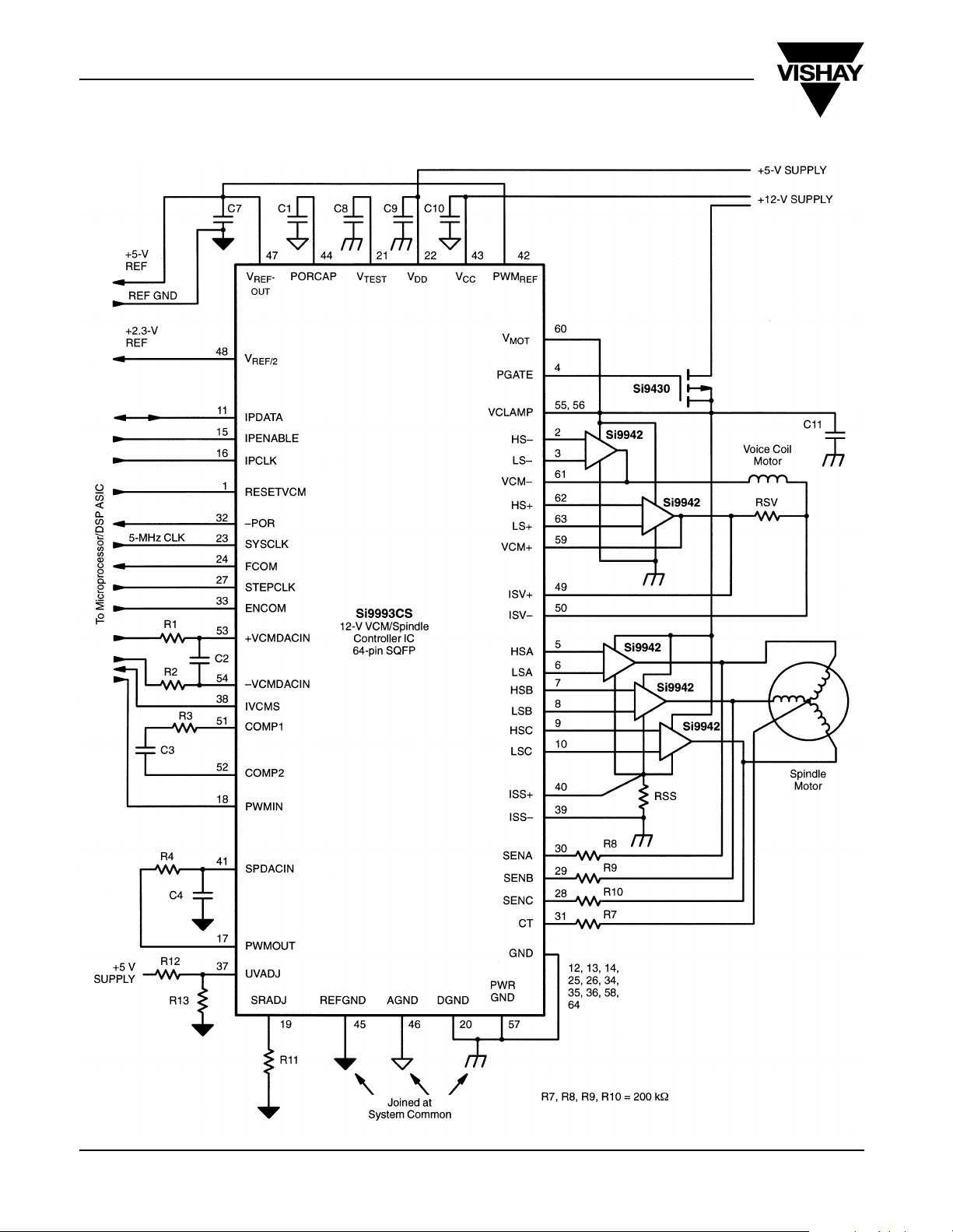
Si9993CS
Vishay Siliconix
APPLICATIONS
S-60752–Rev. A, 05-Apr-99 FaxBack 408-970-5600, request 70653
16 www.siliconix.com
 Loading...