Si9978DW
Configurable H-Bridge Driver
FEATURES
• H-Bridge or Dual Half-Brid ge Operation
• 20- to 40-V Supply
• Static (dc) Operation
DESCRIPTION
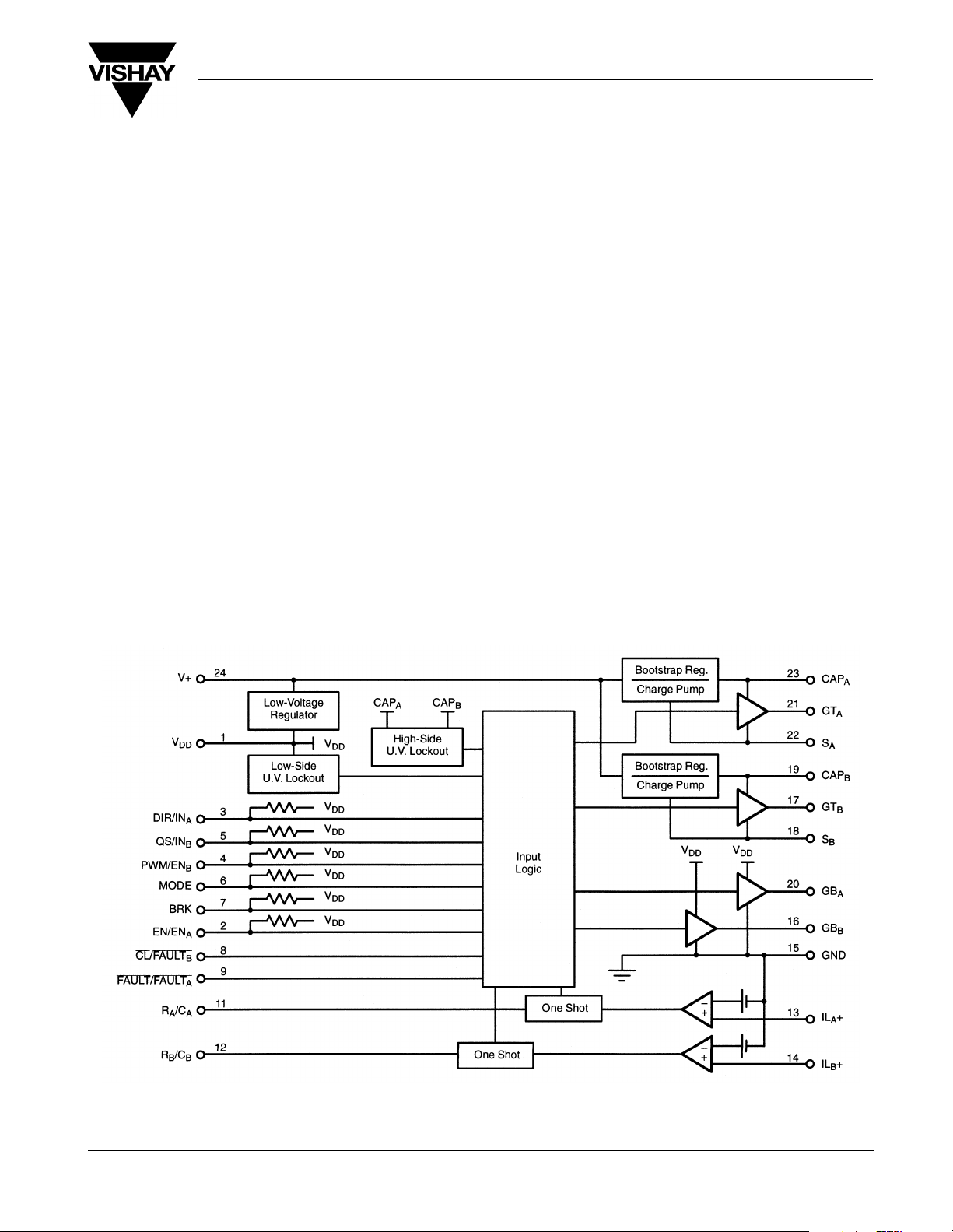
The Si9978DW is an integrated driver for an n-channel
MOSFET H-bridge. The mode control allows operation as
either a full H-bridge driver or as two independent
half-bridges. The DIR/PWM input configuration allows easy
implementation of either sign/magnitude or anti-phase PWM
drive schemes for full H-bridges. Schmitt triggers on the
inputs provide logic signal compatibility and hysteresis for
increased noise immunity. An internal low-voltage regulator
allows the device to be powered directly from a system supply
of 20 to 40 volts. All n-channel gates are driven directly from
low-impedance outputs. The addition of one external
• Cross-Conduction Protected
• Current Limit
• Undervoltage Lockout
• ESD Protected
• Fault Output
capacitor per half -bridge allows in terna l circuitr y to level shift
both the power supply and logic signal for the high-side
n-channel gate drives. Internal charge pumps replace l eak ag e
current lost in the high-side driver cir cuits to provide “stati c”
(dc) operation in any output condition. Protection features
include an undervoltage lockout, cross-conduction prevention
logic, and overcurrent monitors.
The Si9978DW is available in the 24-pin wide-body SOIC
(surface mount) package, specified to operate over the
industrial (-40 to +85°C) temperature range.
Vishay Siliconix
Si9978
FUNCTIONAL BLOCK DIAGRAM
FaxBack 408-970-5600, request 70011 S-60752—Rev. D, 05-Apr-99
www.siliconix.com 1

Si9978DW
Vishay Siliconix
ABSOLUTE MAXIMUM RATINGS
Voltage on pins 2-7 with respect to ground. . . . . . -0.3 to V
DD
+ 0.3 V
Voltage on pin 24 . . . . . . . . . . . . . . . . . . . . . . . . . . . . . . . -0.3 to 50 V
Voltage on pins 17, 19, 21, 23 . . . . . . . . . . . . . . . . . . . . -0.3 to +60 V
Voltage on pins 18, 22 . . . . . . . . . . . . . . . . . . . . . . . . . . . . .-2 to 50 V
Operating Temperature (T
). . . . . . . . . . . . . . . . . . . . . . . - 40 to +85°C
A
Storage Temperature. . . . . . . . . . . . . . . . . . . . . . . . . . . .-65 to 150°C
Maximum Junction Temperature (T
). . . . . . . . . . . . . . . . . . . . . 150°C
J
Power Dissipation . . . . . . . . . . . . . . . . . . . . . . . . . . . . . . . . . 500 mW
RECOMMENDED OPERATING CONDITIONS
V+. . . . . . . . . . . . . . . . . . . . . . . . . . . . . . . . . . . . . . . . . +20 to 40 V
RA, RB. . . . . . . . . . . . . . . . . . . . . . . . . . . . . . . . . . . . . . . . . . . .100 k
DC
Ω
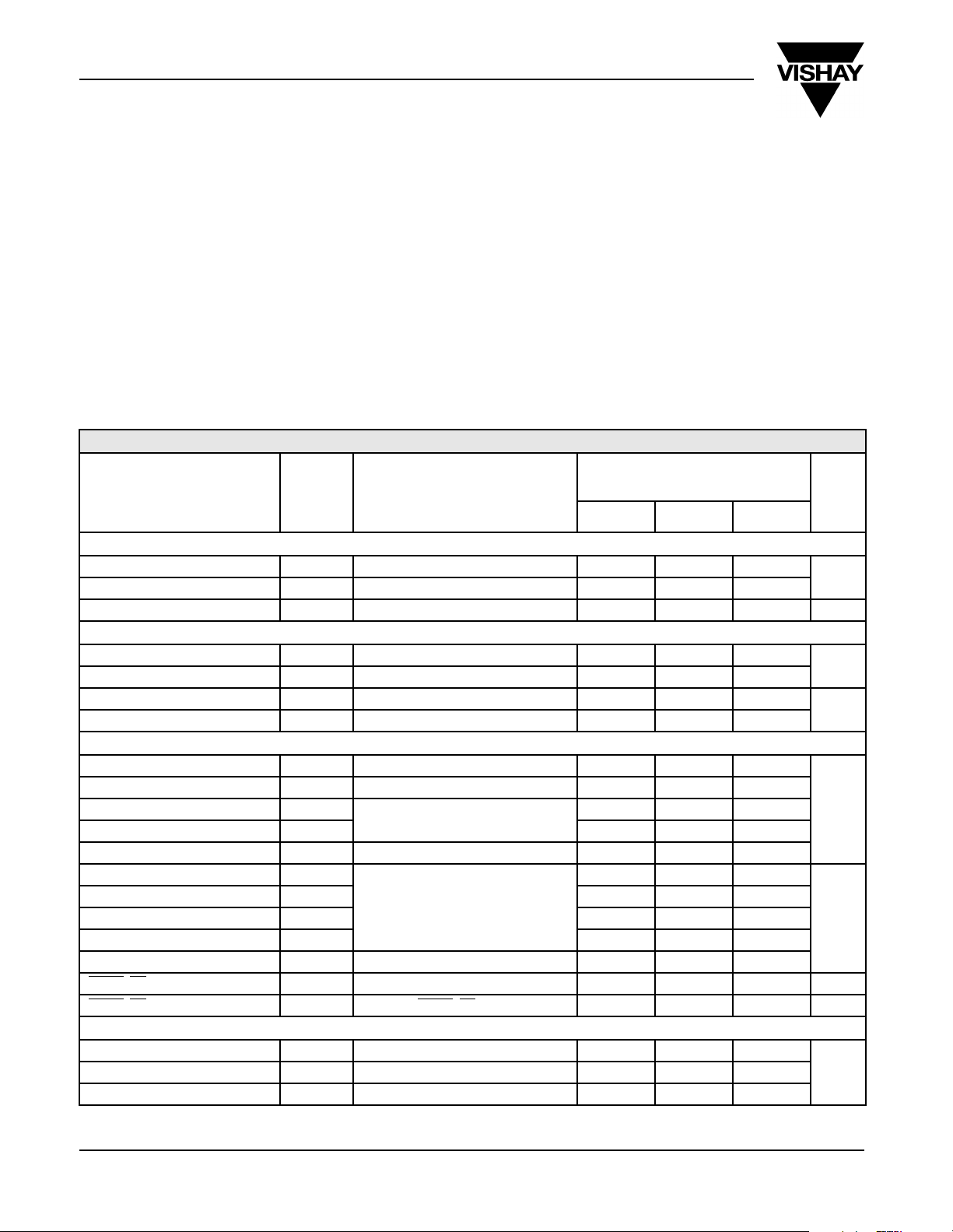
SPECIFICATIONS
Test Conditions
Parameter Symbol
Unless Otherwise Specified
V+ = 20 to 40 V
a
Power
Supply Voltage Range V+ 20 40
Logic Voltage V
DD
Supply Current I+ I
= 0 mA 3 5 mA
DD
14.5 16 17.5
Inputs (DIR, PWM, EN, QS, MODE, BRK)
High-State V
Low-State V
High-State Input Current I
Low-State Input Current I
IH
IL
IH
IL
VIH = V
DD
VIL = 0 V -100 -50 -25
4.0
Outputs
Low-Side Gate Drive, High State V
Low-Side Gate Drive, Low State V
High-Side Gate Drive, High State V
High-Side Gate Drive, Low State V
Capacitor Voltage
c
Low-Side Switching, Rise Time t
Low-Side Switching, Fall Time t
High-Side Switching, Rise Time t
High-Side Switching, Fall Time t
V
GBH
GBL
GTH
GTL
CAP
rL
fL
rH
fH
S
= 0 V
A, B
V+ = 40 V 55
Rise Time = 1 to 10 V
Fall Time = 10 to 1 V
= 600 pF
C
L
Break-Before-Make Time 250
, CL V
FAULT
, CL Leakage Current I
FAULT
OL
OH
IOL = 1 mA 0.4 V
FAULT, CL = V
DD
14 16 17.5
14 16 18
Protection
Low-Side Undervoltage Lockout UVLL 0.8 V
H
High-Side Undervoltage Lockout UVLH S
= 0 V VDD-3.3 V
A, B
Limits
-40 to 85°C
b
Typ
110
50
110
50
0.2 10 µA
DD
0.8
Max
1.0
10
1
1
a
UnitMin
V
V
µA
V
ns
VLow-Side Hysteresis V
S-60752—Rev. D, 05-Apr-99 FaxBack 408-970-5600, request 70011
2 www.siliconix.com
 Loading...