N-Channel Half-Bridge Driver
FEATURES APPLICATIONS
• Single Input for High-Side and Low-Side MOSFETs
• 20- to 40-V Supply
• Static (dc) Operation
• Cross-Conduction Protected
• Undervoltage Lockout
• ESD and Short Circuit Protected
• Fault Feedback
DESCRIPTION
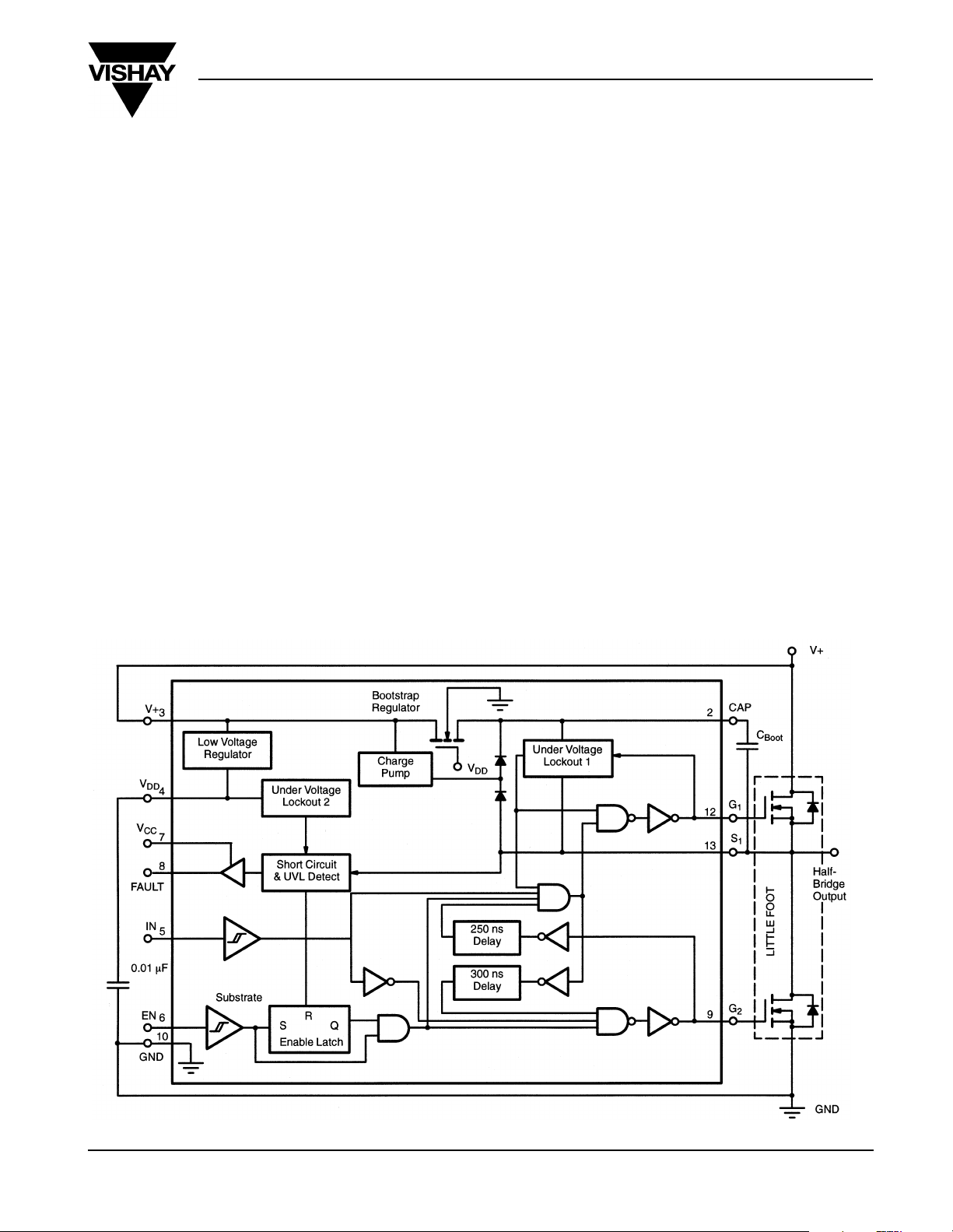
The Si9976DY is an integrated driver for an n-channel
MOSFET half-bridge. Schmitt trigger inputs provide logic
signal compatibility and hysteresis for increased noise
immunity. An internal low-voltage regulator allows the device
to be powered directly from a system supply of 20 to 40 V.
Both half-bridge n-channel gates are driven directly with
low-impedance outputs. Addition of one external capacitor
allows an internal circuit to level shift both the power supply
• Power Supplies
• Motor Drives
• Office Automation
• Computer Peripherals
• Industrial Controllers
• Robotics
• Medical Equipment
and logic signal for the half-bridge high-side n-channel gate
drive. An internal charge pump replaces leakage current lost
in the high-side driver circuit to provide “static” (dc) operation
in any output condition. Protection features include an
undervoltage lockout, cross-conduction prevention logic, and
a short circuit monitor. The Si9976DY is available in the
14-pin SOIC (surface mount) package, specified to operate
over the industrial (-40 to 85°C) temperature range.
Si9976DY
Vishay Siliconix
Si9976
FUNCTIONAL BLOCK DIAGRAM
FaxBack 408-970-5600, request 70016 S-60752-Rev. E, 05-Apr-99
www.siliconix.com 1

Si9976DY
Vishay Siliconix
ABSOLUTE MAXIMUM RATINGS
Voltage on IN, EN (pins 5, 6)
with respect to ground . . . . . . . . . . . . . . . . . . . . . . -0.3 to V
Voltage on V
(pin 7) . . . . . . . . . . . . . . . . . . . . . . . . . . -0.3 to +18 V
CC
Voltage on V+, S1 (pins 3, 13). . . . . . . . . . . . . . . . . . . . -0.3 to +50 V
a
Voltage on CAP, G1
(pins 2, 12). . . . . . . . . . . . . . . . . . -0.3 to +60 V
Peak Output Current . . . . . . . . . . . . . . . . . . . . . . . . . . . . . . . . . .0.5 A
Operating Temperature (T
). . . . . . . . . . . . . . . . . . . . . . . .-40 to 85°C
A
Storage Temperature . . . . . . . . . . . . . . . . . . . . . . . . . . . .-50 to 150°C
DD
+0.3 V
Maximum Junction Temperature (T
b
Power Dissipation
c . . . . . . . . . . . . . . . . . . . . . . . . . . . . . . . . . . . . . . . . . . . 100°C/W
Θ
JA
. . . . . . . . . . . . . . . . . . . . . . . . . . . . . . . . . . . . 1 W
) . . . . . . . . . . . . . . . . . . . . 125°C
J
Notes
a. Internally generated voltage for reference only.
b. Derate 10 mW/°C above 25°C.
c. PC board mounted with no forced air flow.
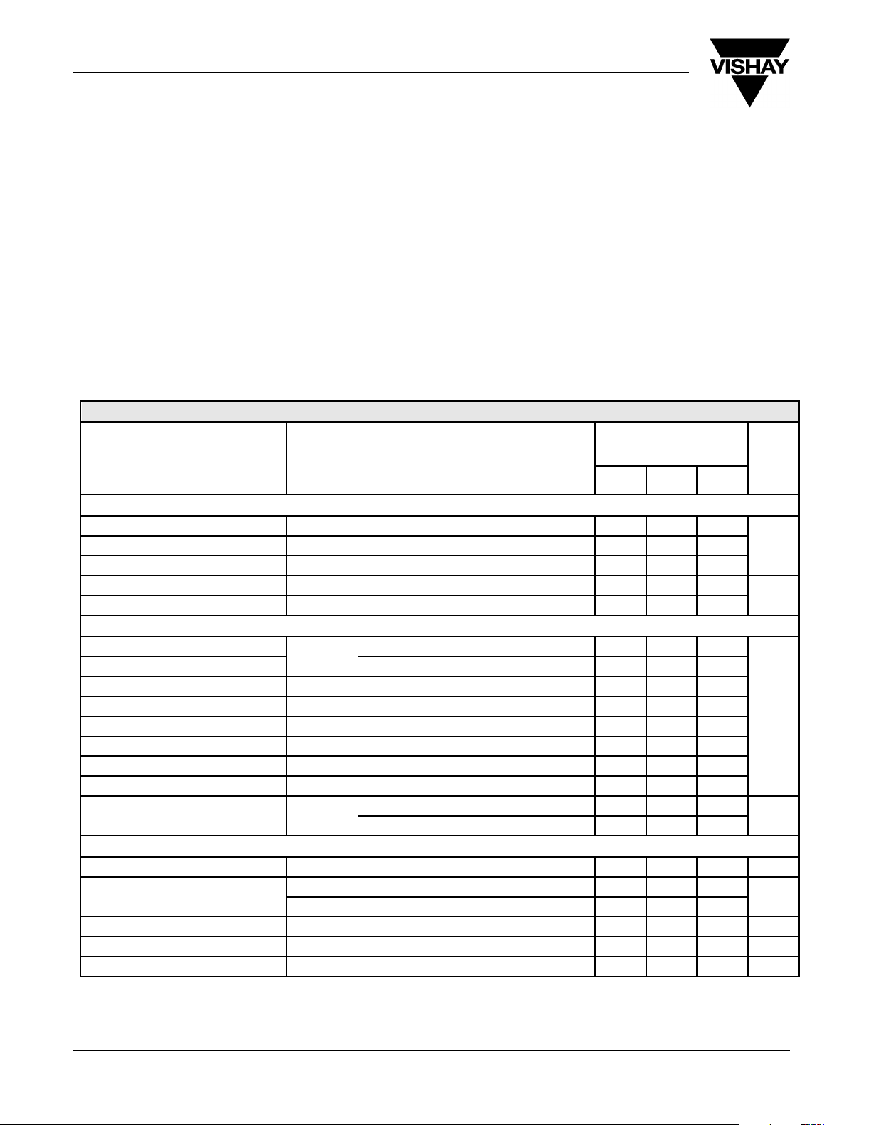
SPECIFICATIONS
Parameter Symbol
a
Test Conditions
UnlessOtherwise Specified
V+ = 20 to 40 V
= Operating Temperature Range
T
A
Limits
D Suffix -40 to 85°C
c
TypbMax
c
UnitMin
Input
Input Voltage High (EN and IN) V
Input Hysteresis Voltage V
Input Curren—-Input Voltage High I
Input Current—Input Voltage Low I
INH
INL
INH
INL
H
(EN and IN) VIN = 15 V 1
(EN and IN) VIN = 0 V -1
4.0
1.0
0.5
Output
Output Voltage High, G1
Output Voltage High, G2
Output Voltage Low, G1 and G2 V
Fault Output Voltage High V
Fault Output Voltage Low V
Undervoltage Lockout 1 UVL1 11
Undervoltage Lockout 2 UVL2 14
Capacitor Voltage
Capacitor Current I
d
V
e
g
OUTH
OUTL
OH
OL
V
CAP
CAP
S1 = V+, I
S1 = GND, I
S1 = GND, I
VCC = 4.5 V, I
VCC = 4.5 V, I
V+ = 40V 55
S1 = GND, V
S1 = GND, V
= -10 mA 10 12
OUT
= -10 mA 12 15
OUT
= 60 mA 1.2 3
OUT
= -0.2 mA 3.5 4
OUT
= 0.6 mA 0.3 1.0
OUT
= 0 V -10
CAP
= 9 V -2
CAP
mA
Supply
V+ Supply Range 20 40 V
V+ Supply Current
Supply Range 4.5 16.5 V
V
CC
Supply Current I
V
CC
Supply Voltage
V
DD
f
I+ (H) G2 High, No Load 1.7 3.5
I+ (L) G2 Low, No Load, S1 = GND 2 4.5
CC
V
DD
VCC = 16.5 V 10 µA
15 16 17.5 V
mA
VInput Voltage Low (EN and IN) V
µA
V
S-60752-Rev. E, 05-Apr-99 FaxBack 408-970-5600, request 70016
2 www.siliconix.com
 Loading...