


12-V Voice Coil Motor Driver
FEATURES
D 1.8-A H-Bridge Output
D Class B Linear Operation
D Externally Programmable Gain and
Bandwidth
DESCRIPTION
The Si9961 is a linear actuator (voice coil motor) driver suitable
for use in disk drive head positioning systems. The Si9961
contains all of the power and control circuitry necessary to
drive the VCM that is typically found in 3
drives and optical disk drives. The driver is capable of
delivering 1.8 A at a nominal supply of 12 V.
The Si9961 provides all necessary functions including a motor
current sense amplifier, a loop compensation amplifier and a
power amplifier featuring four complementary MOSFETs in a
H-bridge configuration. The output crossover protection
ensures no cross-conducting current and true Class B
D Undervoltage Head Retract
D Programmable Retract Current
D Low Standby Current
1
/2-inch hard disk
Si9961
Vishay Siliconix
D Rail-to-Rail Output Swing
D Single 12-V Supply
D System Voltage Monitor with Fault Output
operation during linear tracking. Externally programmable
gain switch at the input summing junction increases the
resolution and dynamic range for a given DAC. The head
retract circuitry can be activated by either an undervoltage
condition or an external command. An external resistor is
required to set the VCM current during retract.
The Si9961 is constructed on a self-isolated BiC/DMOS power
IC process. The IC is available in 24-pin SO package for
operation over the commercial, C suffix (0 to 70_C)
temperature range.
FUNCTIONAL BLOCK DIAGRAM
V
CC
IA2–
I
RET
OA2
4
5
23
V
R
9
6
11
22
10
A2
–
+
Acceleration Error
V
FAULT
RETRACT
Enable
GAIN
SELECT
R
EXT
V
REFVREF–
V
8 R
+
–
Retract
Control
–
+
7 R
A3
R
A4
A5
–
+
V+
818712
Voltage
Monitor
R
V
R
R
Q1
Q2
V
DD
Q3
17
OUTPUT
A
OUTPUT
19
Q4
B
Document Number: 70014
S-20883—Rev. G, 24-Jun-02
R
INHRINL
20161415211332421
I
R
FB
SENSE
OUT
I
SENSE
IN+
I
SENSE
IN–
GND
SA SB
www.vishay.com
1
Si9961
Vishay Siliconix
ABSOLUTE MAXIMUM RATINGS
Voltages Referenced to Common Pin
V+ Supply Range –0.3 V to 16 V. . . . . . . . . . . . . . . . . . . . . . . . . . . . . . . . . . . .
Pin (FAULT
) –0.3 V to VCC + 0.3 V. . . . . . . . . . . . . . . . . . . . . . . . . . . . . . . . . .
Pin (Output A & B, Source A & B) –0.3 V to V
Pin (All Others) –0.3 V to V+ + 0.3 V. . . . . . . . . . . . . . . . . . . . . . . . . . . . . . . .
Maximum Clamp Current
Output A, Output B (Pulsed 10 ms at 10% duty cycle) "1.8 A. . . . . . . . . . . .
Pin (All Others) "20 mA. . . . . . . . . . . . . . . . . . . . . . . . . . . . . . . . . . . . . . . . . .
Storage Temperature –65 to 150_C. . . . . . . . . . . . . . . . . . . . . . . . . . . . . . . . .
DD
+ 0.3 V. . . . . . . . . . . . . . . .
Operating Temperature 0 to 70_C. . . . . . . . . . . . . . . . . . . . . . . . . . . . . . . . . . .
Junction Temperature (T
Power Dissipation (Package)
24-Pin SOIC
b
Thermal Impedance (
24-Pin SOIC 40_C/W. . . . . . . . . . . . . . . . . . . . . . . . . . . . . . . . . . . . . . . . . . . . . .
Notes
a. Device mounted with all leads soldered or welded to PC board.
b. Derate 25 mW/_C above 25_C.
) 150_C. . . . . . . . . . . . . . . . . . . . . . . . . . . . . . . . . . . .
J
a
a
)
JA
3.125 W. . . . . . . . . . . . . . . . . . . . . . . . . . . . . . . . . . . . . . . . . . . .
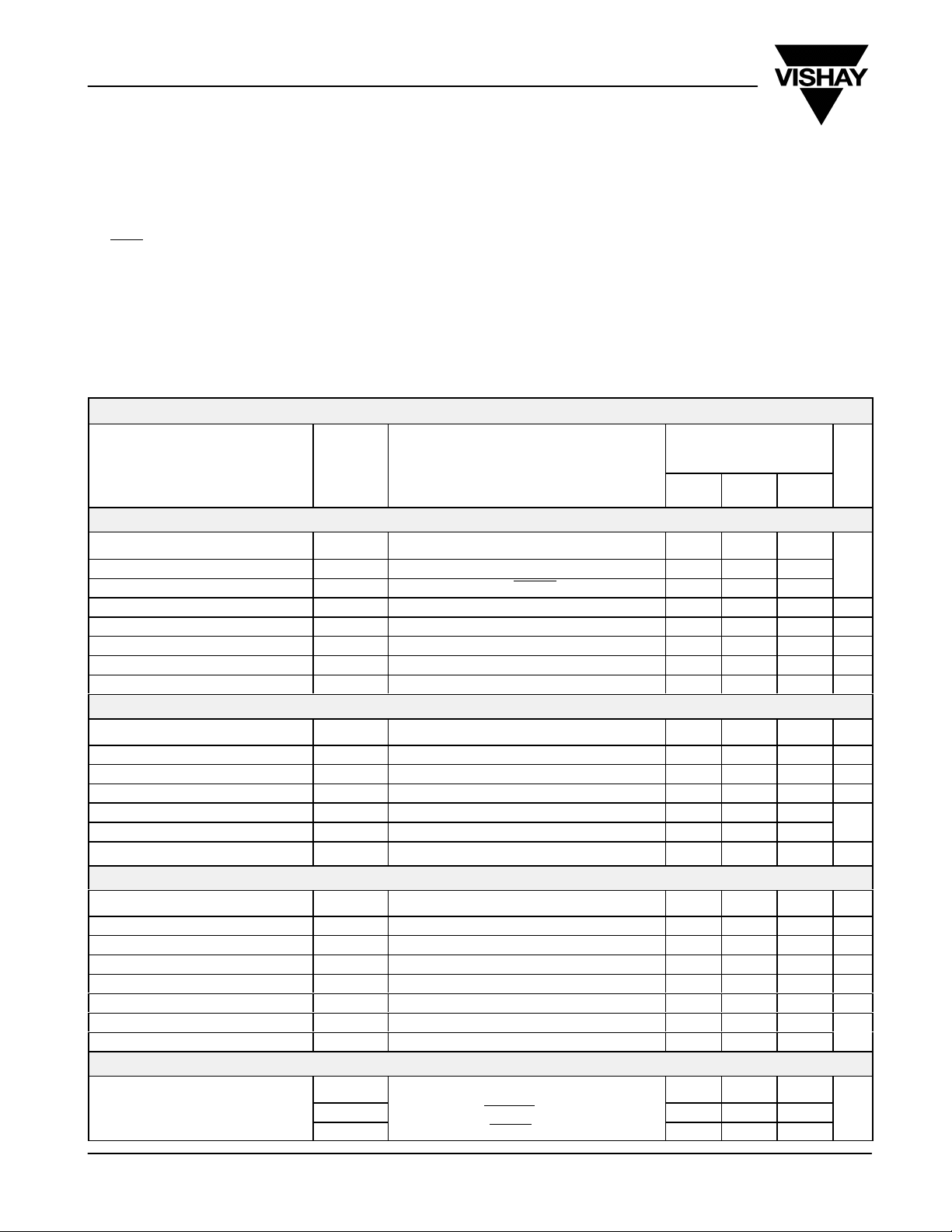
SPECIFICATIONS
T est Conditions
Unless Otherwise Specified
V+ = 12 V "10%, VDD = 11.6 V "10%
V
Parameter Symbol
= 5 V "10%, V
CC
V
REF
= GND = 0 V
REF–
= 5 V "5%
Min
Bridge Outputs (A4, A5)
High Level Output Voltage V
Low Level Output Voltage V
Clamp Diode Voltage V
OH
OL
CL
Amplifier Gain Output V
Dynamic Crossover Current Measured at V
Slew Rate SR 1 V/S
Small Signal Bandwidth (–3 dB) 0.2 MHz
Input Deadband –60 60 mV
IOH = 1.0 A, VDD = 10.2 V, OA2= V
IOL = –1.0 A, OA2 = V
REF
"1 V 8.0 9.1
REF
"1 V 0.6 1.1
IF = 1.0 A, ENABLE = High 2.5
= V
RANGE
"2 V 12 16 18 V/V
REF
DD
A2, Loop Compensation Amplifier
Input Offset Voltage V
Input Bias Current I
Unity Gain Bandwidth R
Slew Rate SR 1 V/s
Power Supply Rejection Ratio PSRR @ 10 kHz 50
Open Loop Voltage Gain A
Output Voltage Swing V
OS
B
VOL
Gain Select = High, IA
= 10 k, C
LOAD
O
R
LOAD
LOAD
= 10 k to V
–
= 5 V –50 50 nA
2
= 100 pF to V
REF
REF
V
REF
A3, Current Sense Amplifier
Input Offset Voltage V
Input Impedance R
Small Signal Bandwidth (–3 dB) R
Common Mode Rejection Ratio CMRR @ 5 kHz 50 dB
Slew Rate SR 2 V/s
Gain 3.9 4 4.1 V/V
Input Common-Mode Voltage Range V
Output Voltage Swing V
OS
CM
I
IN
LOAD
IN+ to I
SENSE
= 10 k, C
LOAD
IN– 5 k
SENSE
= 100 pF to V
REF
T o GND –0.3 2
R
O
LOAD
= 10 k, C
= 100 pF to V
LOAD
REF
V
REF
Supply
I
CC Static, No Load
Supply Current (Normal)
I
V+
I
DD
RETRACT = High 2 5
ENABLE = Low
Limits
C Suffix 0 to 70_C
b
TypaMaxbUnit
10 mA
–8 8 mV
1 MHz
80
–2 V
–5 5 mV
1 MHz
–2 V
5 13
REF
REF
0.01
+2 V
+2
V
dB
V
mA
www.vishay.com
2
Document Number: 70014
S-20883—Rev. G, 24-Jun-02

Si9961
Vishay Siliconix
SPECIFICATIONS
T est Conditions
T est Conditions
Unless Otherwise Specified
Unless Otherwise Specified
V+ = 12 V "10%, VDD = 11.6 V "10%
V+ = 12 V "10%, VDD = 11.6 V "10%
V
V
= 5 V "10%, V
= 5 V "10%, V
CC
Parameter UnitMax
Symbol
CC
V
V
REF
REF
= GND = 0 V
= GND = 0 V
REF–
REF–
= 5 V "5%
= 5 V "5%
Min
Supply
I
CC Static, No Load
Supply Current (Standby)
VDD Range V
VCC Range V
V+ Range V+ 10.8 12 13.2
I
V+
I
DD
DD
CC
RETRACT = High 0.2 0.4
ENABLE = High
Normal Mode 10.2 11.6 13.2
Retract Mode 2.0 14
Gain Select Switch
RFB Switch Resistance 108 240
R
Switch Resistance
INH
R
Switch Resistance 810 1800
INL
V
(EXT)
REF
Input Current I
External Voltage Range V
REF
REF
IA2– = 5 V
OA2 = V
REF
Power Supply Monitor
VCC Undervoltage Threshold V
Hysteresis 40 mV
V+ Undervoltage Threshold V
Hysteresis 100 mV
= 5.0 V 3.82 4.12 4.42 V
REF
= 5.0 V 9.1 9.8 10.6 V
REF
Gain Select, RETRACT, ENABLE Input
Input High V oltage V
Input Low Voltage V
Input High Current I
Input Low Current I
IH
IL
IH
IL
VIN = 5 V –1 1
VIN = 0 V –1 1
FAULT Output
Output High Voltage V
Output Low Voltage V
Output High Sourcing Current I
OH
OL
OHS
IOH = –100 A
IOL = 1.6 mA 0.25 0.50
V
= 0 V 400 1100 A
OUT
RETRACT Current Control (RETRACT = Low, Output Current from A to B)
I
Bias Voltage V(I
RET
Retract Output Pull-Up Voltage V
Retract Output Pull-Down Current I
Maximum Emergency Retract Current I
Retract Current VDD Supply Rejection Ratio VDD = 2 V to 14 V, R
Retract Current Temperature Coefficient VDD = 10 V, R
Notes
a. Typical values are for DESIGN AID ONLY, not guaranteed nor subject to production testing.
b. The algebraic convention whereby the most negative value is a minimum and the most positive a maximum.
) VDD = 10 V, R
RET
OUT A
OUTB
(Max) VDD = 2 V, V
OUTB
VDD = 10 V, V
RET
VDD = 2.5 V to 14 V, I
= 5 V R
OUTB
R
= 0.5 , TA = 25_C
SB
= 0.7 V R
OUTB
RET
RET
= 3.74 k 0.66
= 30 mA VDD –1
OUTA
= 3.74 k
RET
= < 10 , RSB = 0.5 , 40
= 3.74 k 3.0 %/V
RET
= 3.74 k –0.3 %/_C
Limits
C Suffix 0 to 70_C
b
4.5 5 5.5
0.15 0.40 0.65 mA
4.75 5 5.25 V
3.5
V
CC
–0.8
22 30 38
a
Typ
0.8 1.6
135 300
V
CC
–0.33
b
0.01
1.5
mA
V
V
A
V
V
mA
mA
Document Number: 70014
S-20883—Rev. G, 24-Jun-02
www.vishay.com
3
 Loading...