

Page 1
查询SI9912供应商
Half-Bridge MOSFET Driver for Switching Power Supplies
FEATURES APPLICATIONS
Si9912
Vishay Siliconix
D 4.5- to 5.5-V Operation
D Undervoltage Lockout
D 250-kHz to 1-MHz Switching Frequency
D Shutdown Quiescent Current <5 mA
D One Input PWM Signal Generates Both Drive
D Multiphase Desktop CPU Supplies
D Single-Supply Synchronous Buck Converters
D Mobile Computing CPU Core Power Converters
D Standard-Synchronous Converters
D High Frequency Switching Converters
D Bootstrapped High-Side Drive
D Operates from 4.5- to 30-V Supply
D TTL/CMOS Compatible Input Levels
D 1-A Peak Drive Current
D Break-Before-Make Circuit
DESCRIPTION
The Si9912 is a dual MOSFET high-speed driver with
break-before-make. It is designed to operate in high frequency
dc-dc switchmode power supplies. The high-side driver is
bootstrapped to handle the high voltage slew rate associated
with “floating” high-side gate drivers. Each driver is capable of
switching a 3000-pF load with 60-ns propogation delay and
25-ns transition time. The Si9912 comes with an internal
break-before-make feature to prevent shoot-through current in
the external MOSFETs. A shutdown pin is used to enable the
driver. When disabled, the quiescent current of the driver is
less than 5 mA.
The Si9912 is available in both standard and lead (Pb)-free, 8-pin
SOIC packages for operation over the industrial operation range
(−40_C to 85_C).
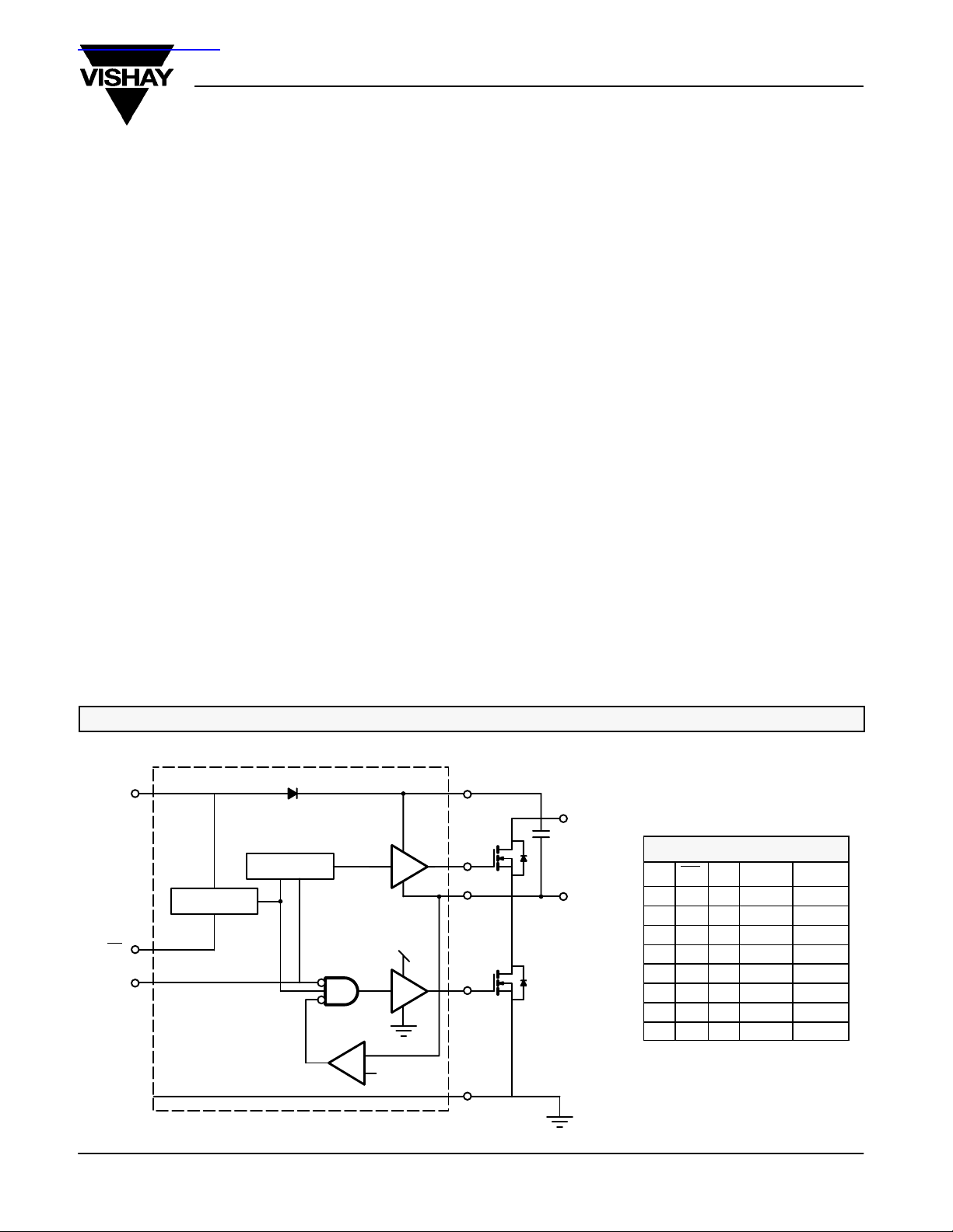
FUNCTIONAL BLOCK DIAGRAM AND TRUTH TABLE
V
DD
Undervoltage
SD
IN
Document Number: 71311
S-40134—Rev. B, 16-Feb-04
D1
Level Shift
BOOT
V
DC
Q
1
OUT
H
V
S
V
DD
OUT
L
+
V
−
BBM
GND
C
BOOT
OUTPUT
Q
2
TRUTH TABLE
VSSD IN V
L L L L L
L L H L L
L H L H L
L H H L H
H L L L L
H L H L L
H H L L L
H H H L H
OUTLVOUTH
www.vishay.com
1
Page 2
Si9912
Vishay Siliconix
ABSOLUTE MAXIMUM RATINGS (TA = 25_C UNLESS OTHERWISE NOTED)
Parameter Symbol Limit Unit
Low Side Driver Supply Voltage V
Input Voltage on IN V
Shutdown Pin Voltage V
Bootstrap Voltage V
High Side Driver (Bootstrap) Supply Voltage V
Operating Junction Temperature Range T
Storage Temperature Range T
Power Dissipation (Note a and b) P
Thermal Impedance q
BOOT
BOOT
DD
SD
stg
JA
IN
− V
J
D
S
Lead Temperature (soldering 10 Sec) 300 °C
Notes
a. Device mounted with all leads soldered to P.C. Board
b. Derate 8.3 W/_C above 25_C
Stresses beyond those listed under “Absolute Maximum Ratings” may cause permanent damage to the device. These are stress ratings only, and functional operation
of the device at these or any other conditions beyond those indicated in the operational sections of the specifications is not implied. Exposure to absolute maximum rating
conditions for extended periods may affect device reliability.
7.0
−0.3 to VDD +0.3
−0.3 to VDD +0.3
35.0
7.0
−40 to 125
−40 to 150
830 mW
125 °C/W
_
_C
V
RECOMMENDED OPERATING CONDITIONS
Parameter Symbol Limit Unit
Bootstrap Voltage (High-Side Drain Voltage) V
Logic Supply V
Bootstrap Capacitor C
Ambient Temperature T
SPECIFICATIONS
Test Conditions Unless Specified
Parameter Symbol
Power Supplies
VDD Supply V
I
Supply I
DD
I
Supply I
DD
I
Supply I
DD
I
Supply I
DD
I
Supply I
DD
I
Supply
DD
DD1(en)
DD2(en)
DD3(dis)
DD4(en)
DD5(dis)
I
DD(en)
I
DD(dis)
Boot Strap Current I
Reference Voltage
Break-Before-Make Reference Voltage V
Logic Inputs (SD, IN)
Input High V
Input Low V
Undervoltage Lockout
VDD Undervoltage V
VDD Undervoltage Hysteresis V
DD
BOOT
BBM
IH
IL
UVL
HYST
V
SD = H, IN = X, VS = 25 V, V
SD = L, IN = X, VS = 25 V, V
FIN = 300 kHz, SD = High, Driving Si4412DY 9 mA
FIN = 300 kHz, SD = Low, Driving Si4412DY 3 mA
V
VDD = 4.5 to 5.5 V
= 4.5 to 30 V, TA = −40 to 85_C
BOOT
SD = H, IN = H, VS = 0 V 1000
SD = H, IN = L, VS = 0 V 500
SD = L, IN = X, VS = 0 V 5
= 30 V 200
BOOT
= 30 V 5
BOOT
= 30 V, VS = 25 V, V
BOOT
= High 0.9 3 mA
OUTH
VDD Rising 3.7 4.3
BOOT
DD
BOOT
A
4.5 to 30
4.5 to 5.5
100 n to 1 m F
−40 to 85 _C
Limits
a
Min
4.5
1.1 3 V
0.7 V
DD
−0.3 0.3 V
Typ
0.4
b
a
Max
VDD + 0.3
DD
V
Unit
mA
V
V
www.vishay.com
2
Document Number: 71311
S-40134—Rev. B, 16-Feb-04
Page 3
SPECIFICATIONS
VDD =
V
Si9912
Vishay Siliconix
Parameter Symbol
Test Conditions Unless Specified
VDD = 4.5 to 5.5 V
= 4.5 to 30 V, TA = −40 to 85_C
V
BOOT
Min
Limits
a
Typ
b
Bootstrap Diode
Diode Forward Voltage VF
D1
Forward Current = 100 mA 0.8 1 V
Output Drive Current
OUTH Source Current I
OUTH Sink Current I
OUTL Source Current I
OUTL Sink Current I
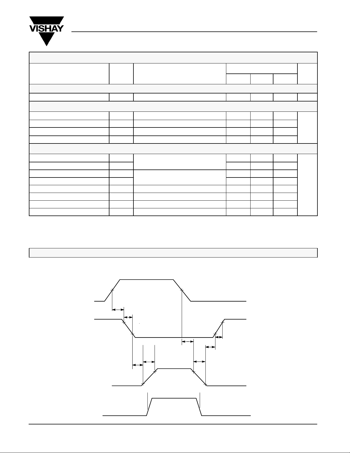
Timing (C
LOAD
= 3 nF)
OUTL Off Propagation Delay t
OUTL On Propagation Delay t
OUTH Off Propagation Delay t
OUTH On Propagation Delay t
OUTL Turn On Time t
OUTL Turn Off Time t
OUTH Turn On Time t
OUTH Turn Off Time t
Notes
a. The algebraic convention whereby the most negative value is a minimum and the most positive a maximum, is used in this data sheet.
b. Typical values are for DESIGN AID ONLY, not guaranteed nor subject to production testing.
OUT(H+)
) V
OUT(H−
) VDD = 4.5 V, V
OUT(L+
−) VDD = 4.5 V, V
OUT(L
pdl(OUTL)
pdh(OUTL)
pdl(OUTH)
pdh(OUTH)
r(OUTL)
f(OUTL)
r(OUTH)
f(OUTH)
V
BOOT
− VS = 3.7 V, V
BOOT
− V
= 3.7 V, V
S
− V
= 2 V −0.4
OUTH
OUTH
OUTL
OUTL
S
− VS = 1 V 0.4
= 2 V −0.4
= 1 V 0.6
4.5
V
− VS = 4.5 V
BOOT
OUTL = 10 to 90% 25
OUTL = 90 to 10% 25
OUTH − V
OUTH − V
= 10 to 90% 30
S
= 90 to 10% 20
S
30
20
30
20
Max
a
Unit
A
ns
TIMING WAVEFORMS
IN
OUT
L
OUT
H
V
S
50% 50%
t
pdh(OUTL)
t
90%
f(OUTL)
10%
t
t
t
pdh(OUTH)
r(OUTH)
90% 90%
10% 10%
pdl(OUTH)
10%
90%
t
f(OUTH)
t
r(OUTL)
t
pdl(OUTL)
Document Number: 71311
S-40134—Rev. B, 16-Feb-04
www.vishay.com
3
Page 4

Si9912
Vishay Siliconix
PIN CONFIGURATION
SO-8
OUT
GND
SD
1
H
2
IN
3
4
Top View
V
8
S
BOOT
7
V
6
DD
OUT
5
L
PIN DESCRIPTION
Pin Number Name Function
1 OUT
2 GND Ground supply
3 IN CMOS level input signal. Controls both output drives.
4 SD Shutdown pin
5 OUT
6 V
7 BOOT Floating bootstrap supply for the upper MOSFET
8 V
DD
Output drive for upper MOSFET.
H
Output drive for lower MOSFET.
L
Input power supply
Floating GND for the upper MOSFET. V
S
is connected to the buck switching node and the source side of the upper MOSFET.
S
ORDERING INFORMATION
Part Number Temperature Range Package
Si9912DY
Si9912DY-T1
Si9912DY-T1—E3 (Lead (Pb)-Free)
−40 to 85_C
Bulk
Tape and Reel
TYPICAL WAVEFORMS
Driver On Switch Delay
V
OUT
OUT
IN
www.vishay.com
4
CL = Si4412DY CL = Si4412DY
S
H
L
Si9912 tr, tf, tpd
Eval Kit Temperature Range Board Type
Si9912DB −40 to 85_C Surface Mount
Driver Off Switch Delay
V
S
OUT
H
See Figure 1 See Figure 1
OUT
L
IN
Si9912 tr, tf, tpd
Document Number: 71311
S-40134—Rev. B, 16-Feb-04
Page 5

TYPICAL CHARACTERISTICS (25_C UNLESS NOTED)
Si9912
Vishay Siliconix
30
10
Current (mA)
1
1
0
−1
−2
−3
Output Voltage Drop (V)
−4
IDD Supply Current vs. Frequency
See Figure 1
100
Frequency (kHz)
V
0.5 A
See Figure 3
OUT(H+)
1 A
vs. Supply
1.5 A
Rise and Fall Time vs. C
50
See Figure 2
40
t
30
20
Rise and Fall times (ns)
10
100010
0
0.3 101
5
4
3
2
Output Voltage Drop (V)Output Voltage Drop (V)
1
See Figure 3
1 A
0.5 A
f(OUTL)
Load Capacitance (nF)
V
OUT(H−)
1.5 A
vs. Supply
t
r(OUTL)
3
2 A
LOAD
t
r(OUTH)
t
f(OUTH)
−5
3.0 3.5 4.0 4.5 5.0 5.5 6.0
0
0.5 A
−1
1 A
−2
−3
−4
Output Voltage Drop (V)
−5
See Figure 3
−6
4.0 4.5 5.0 5.5 6.0
Document Number: 71311
S-40134—Rev. B, 16-Feb-04
0
3.0 3.5 4.0 4.5 5.0 5.5 6.0
Supply Voltage (V) Supply Voltage (V)
V
vs. Supply V
OUT(L+)
1.5 A
2 A
Supply Voltage (V) Supply Voltage (V)
2.5
See Figure 3
2.0
1.5
1.0
0.5
0.0
4.0 4.5 5.0 5.5 6.0
OUT(L−)
vs. Supply
2 A
1.5 A
1 A
0.5 A
www.vishay.com
5
Page 6

Si9912
Vishay Siliconix
TYPICAL CHARACTERISTICS (25_C UNLESS NOTED)
V
0
−1
−2
−3
Output Voltage Drop (V)
−4
−5
See Figure 3
−50 −25 0 25 50 75 100
V
0
−1
−2
−3
Output Voltage Drop (V)
−4
vs. Temperature
OUT(H+)
0.5 A
1 A
Temperature (_C)
vs. Temperature V
OUT(L+)
2 A
See Figure 3
0.5 A
1 A
1.5 A
V
5
See Figure 3
4
3
2 A
2
Output Voltage Drop (V)Output Voltage Drop (V)
1
0
−50 −25 0 25 50 75 100
2.0
See Figure 3
1.5
1.0
0.5
2 A
1.5 A
1 A
0.5 A
vs. Temperature
OUT(H−)
Temperature (_C)
vs. Temperature
OUT(L−)
1.5 A
1 A
0.5 A
−5
−50 −25 0 25 50 75 100
Temperature (_C) Temperature (_C)
THEORY OF OPERATION
Break-Before-Make Function
The Si9912 has an internal break-before-make function to
ensure that both high-side and low-side MOSFETs are not
turned on at the same time. The high-side drive (OUT
turn on until the low-side gate drive voltage (measured at the
OUTL pin) is less than V
, thus ensuring that the low-side
BBM
MOSFET is turned off. The low-side drive (OUT
on until the voltage at the MOSFET half-bridge output
(measured at the VS pin) is less than V
, thus ensuring that
BBM
the high-side MOSFET is turned off.
www.vishay.com
6
) will not
H
) will not turn
L
0.0
−50 −25 0 25 50 75 100
Under Voltage Lockout Function
The Si9912 has an internal under-voltage lockout feature to
prevent driving the MOSFET gates when the supply voltage (at
) is less than the under-voltage lockout specification
V
DD
(V
). This prevents the output MOSFETs from being turned
UVL
on without sufficient gate voltage to ensure they are fully on.
There is hysteresis included in this feature to prevent lockout
from cycling on and off.
Document Number: 71311
S-40134—Rev. B, 16-Feb-04
Page 7

Si9912
Vishay Siliconix
Bootstrap Supply Operation
(see Functional Block Diagram)
The power to drive the high-side MOSFET (Q2) gate comes
from the bootstrap capacitor (C
). This capacitor charges
BOOT
through D1 during the time when the low-side MOSFET is on
(VS is at GND potential), and then provides the necessary
charge to turn on the high-side MOSFET
. C
BOOT
should be
sized to be greater than ten times the high-side MOSFET gate
capacitance, and large enough to supply the bootstrap current
) during the high-side on time, without significant voltage
(I
BOOT
droop.
Shutdown (SD)
(shutdown input, active low)
When this pin is high, the IC operates normally. When this pin
is low, both high- and low-side MOSFETs are turned off .
APPLICATIONS
Layout Considerations
There are a few critical layout considerations for these parts.
Firstly, the IC must be decoupled as closely as possible to the
power pins. Secondly the IC should be placed physically close
to the high- and low-side MOSFETs it is driving. The major
consideration is that the MOSFET gates must be charged or
discharged in a few nanoseconds, and the peak current to do
this is of the order of 1 A. This current must flow from the
decoupling and bootstrap capacitors to the IC, and from the
output driver pin to the MOSFET gate, returning from the
MOSFET source to the IC. The aim of the layout is to reduce
the parasitic inductance of these current paths as much as
possible. This is accomplished by making these traces as
short as possible, and also running trace and its current return
path adjacent to each other.
+V
DC
678
5
PWM IN
Enable
0.1 mF
4
V
DD
+5 V
5
123
678
123
8
S
7
6
5
L
C2
0.1 mF
C1
0.1 mF
4
U1
1
OUT
H
2
GND
3
IN
4
SD
BOOT
V
OUT
Si9912
Q1
Si4412
Q2
Si4412
GND
C3
L1
15 mH
1 mF
C5
GND
15 mF
C4
GND
+
R
LOAD
FIGURE 1. Typical Applications Schematic Circuit Used to Obtain Typical Rising and Falling Switching Waveforms
Document Number: 71311
S-40134—Rev. B, 16-Feb-04
www.vishay.com
7
Page 8
Si9912
Vishay Siliconix
+5 V
U1
PWM IN
1
OUT
H
2
GND
3
IN
4
SD
V
BOOT
V
DD
OUT
8
S
7
6
5
L
Si9912
C2
0.1 mF
GND
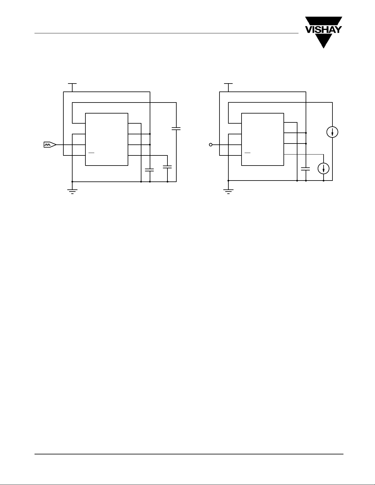
FIGURE 2. Capacitive Load Test Circuit Used to Measure
Rise and Fall Times vs. Capacitance
C
LOAD
C8
C
LOAD
C9
+5 V
U1
Input
1
OUT
H
2
GND
3
IN
4
SD
V
BOOT
V
DD
OUT
S
L
Si9912
GND
FIGURE 3. Load Test Schematic Circuit Used to
Measure Driver Output Impedance
8
7
6
5
ISRC
C2
0.1 mF
ISRC
www.vishay.com
8
Document Number: 71311
S-40134—Rev. B, 16-Feb-04
 Loading...