

查询SI9717供应商
Battery Disconnect Switch
FEATURES
D 6- to 18-V Operation
D Separate Logic Voltage Input
D Undervoltage Lockout (UVL) @ VL = 3 V
D Shutdown Control Capability
D Safe Power Down
DESCRIPTION
Si9717
Vishay Siliconix
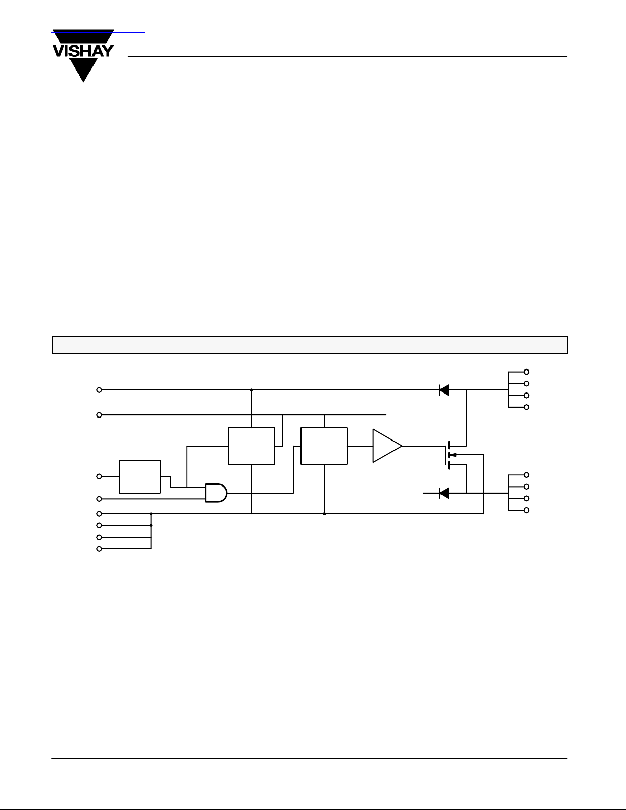
The is a reverse blocking switch for battery disconnect
applications. It is an integrated solution for multiple battery
technology designs or designs that require isolation from the
power bus during charging. The is available in a 16-pin SOIC
package and is rated for the commercial temperature range of
0 to 70_C.
FUNCTIONAL BLOCK DIAGRAM
CBP
CP
ENABLE
GND
7
10
Charge
Pump
Under
6
Voltage
Detect
11
IN
1
8
9
16
The Si9717 is available in both standard and lead (Pb)-free
packages.
2
3
4
A
5
Level
Shift
12
13
14
B
15
ABSOLUTE MAXIMUM RATINGS
Voltage Referenced to GND
V
, V
A
V
IN
V
ENABLE
B
−0.3 to 20 V. . . . . . . . . . . . . . . . . . . . . . . . . . . . . . . . . . . . . . . . . . . . . . .
−0.3 to 10 V. . . . . . . . . . . . . . . . . . . . . . . . . . . . . . . . . . . . . . . . . . . . . . . . . .
−0.3 to 10 V. . . . . . . . . . . . . . . . . . . . . . . . . . . . . . . . . . . . . . . . . . . . . .
RECOMMENDED OPERATING RANGE
VA, VB (see note) 6 to 18 V. . . . . . . . . . . . . . . . . . . . . . . . . . . . . . . . . . . . . . . . .
V
IN
(continuous) 0 to 4 A. . . . . . . . . . . . . . . . . . . . . . . . . . . . . . . . . . . . . . . . . . .
I
AB
x VA (continuous) 0 to 40 W. . . . . . . . . . . . . . . . . . . . . . . . . . . . . . . . . . . . .
I
AB
Minimum Cycle Time (turn-on to turn-on) 10 ms. . . . . . . . . . . . . . . . . . . . . . .
V
ENABLE
Document Number: 70023
S-40743—Rev. D, 19-Apr-04
Storage Temperature −65 to 125_C. . . . . . . . . . . . . . . . . . . . . . . . . . . . . . . . . .
Power Dissipation 2 W. . . . . . . . . . . . . . . . . . . . . . . . . . . . . . . . . . . . . . . . . . . . .
Notes: Device mounted with all leads soldered to PC board.
Operating Temperature 0 to 70_C. . . . . . . . . . . . . . . . . . . . . . . . . . . . . . . . . . .
0 to 5 V. . . . . . . . . . . . . . . . . . . . . . . . . . . . . . . . . . . . . . . . . . . . . . . . . . . . . .
0 to 5 V. . . . . . . . . . . . . . . . . . . . . . . . . . . . . . . . . . . . . . . . . . . . . . . . . .
Junction Temperature 0 to 150_C. . . . . . . . . . . . . . . . . . . . . . . . . . . . . . . . . . .
Notes:
a. is functional at V
specification.
, VB = 5 to 6 V with higher supply current. See I
A
www.vishay.com
A(on)
1
Si9717
Unless Otherwise Specified
ENABLE = 5 V, VA = 10 V, RL = 5 W
Setup Time
m
Vishay Siliconix
SPECIFICATIONS
T est Conditions
Unless Otherwise Specified
Parameter Symbol
On-Resistance R
Leakage Current I
IN Low Threshold V
IN High Threshold V
IN Input Current I
Turn-On Delay IN to A or B t
Turn-Off Delay IN to A or B t
ENABLE Low Threshold V
ENABLE High Threshold V
ENABLE Input Current I
Setup Time
from ENABLE to Switch
On-State Drain I
Off-State Drain I
Notes:
a. Room = 25_C, Full = as determined by the operating temperature suffix.
b. The algebraic convention whereby the most negative value is a minimum and the most positive a maximum, is used in this data sheet.
c. Typical values are for DESIGN AID ONLY, not guaranteed nor subject to production testing.
d. Tested at room temperature, high temperature guaranteed by statistical data correlation techniques.
AB
AB(off)
IN(L)
IN(H)
IN(H)
ON(IN)
OFF(IN)
ENABLE(L)
ENABLE(H)
ENABLE(H)
t
ENABLE(H)
A(on)
A(off)
AB Shorted, VA = 10 V, V
AB Shorted, VA = 5 V, V
AB Shorted, VA = 10 V, V
6 V x VA x 18 V
C
= 0.1 mF, CP = 0.02 mF
VDD
VA = 10 V, IA = 1 A Room 0.06 W
VA = 16 V, VB = 0 V Room 10 mA
VIN = 5.0 V Full 1 mA
ENABLE = 5 V, VA = 10 V, RL = 5 W
VA = 10 V, VIN = 0 V, Test Circuit 2 Room 2.0
Test Circuit 1
V
= 5 V Full 50 mA
ENABLE
VA = 6 V, VIN = 0 V, Test Circuit 2 Full 10
= 5 V Full 60
ENABLE
= 5 V Full 300
ENABLE
= 0 V Full 10
ENABLE
TempaMinbTypcMaxbUnit
Full 1
Full 4.0
Full 10
Full 10
Full 3.0
Full 4.4
Limits
d
V
ms
V
ms
mA
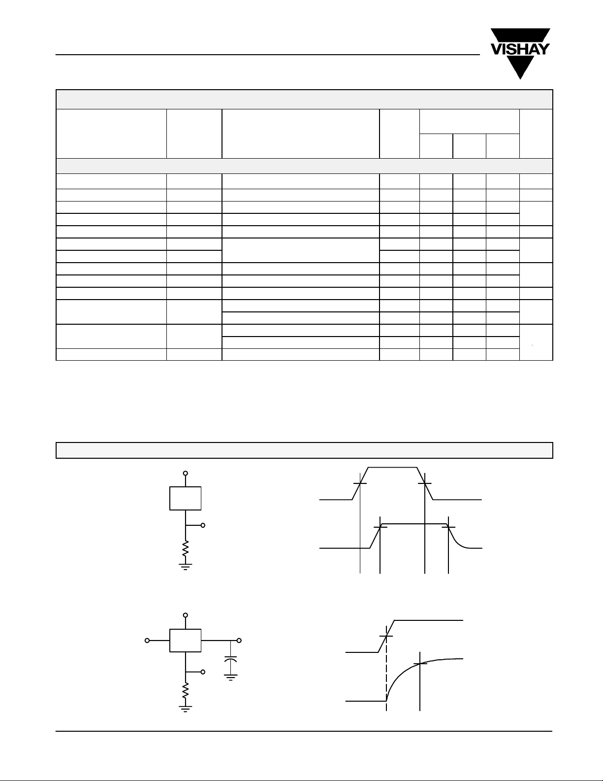
TEST CIRCUITS
5 V CP
10 V
A
0 V
B
5 W
Test Circuit 1
A
0.02 mF
B
10 W
Test Circuit 2
50% 50%
V
IN
90% 90%
V
B
t
ON(IN)
5 V
V
ENABLE
0 V
V
CP
50%
t
ENABLE
t
OFF(IN)
VA + 8.5 V
www.vishay.com
2
Document Number: 70023
S-40743—Rev. D, 19-Apr-04

PIN CONFIGURATION, TRUTH TABLE AND ORDERING INFORMATION
Si9717
Vishay Siliconix
TRUTH TABLE
ENABLE IN Switch Controller State Switch
0 0 Inactive X
0 1 Inactive X
1 0 Set-Up Off
1 1 Active On
ORDERING INFORMATION
Part Number Temperature Range Package
Si9717CY
Si9717CY-T1 0 to 70_C SOIC-16
Si9717CY-T1—E3
GND GND
AB
AB
AB
A
ENABLE
CBP
GND GND
SOIC-16
1
2
3
4
6
7
8
Top View
PIN DESCRIPTION
Pin Number Symbol Description
1, 8, 9, 16 GND Common connection for negative battery terminals.
2, 3, 4, 5 A A-terminal of the battery switch, bidirectional.
6 ENABLE Logic input, ENABLE. Activates charge pump and switch drive logic.
7 CBP Internally generated logic power supply, VDD. Requires external bypass capacitor connected to pin 8.
10 CP Charge pump output terminal. Requires external capacitor connected to pin 9.
11 IN Logic input, IN. A high level turns on the switch.
12, 13, 14, 15 B B-terminal of the battery switch, bidirectional.
16
15
14
13
B
125
IN
11
CP
10
9
APPLICATION DIAGRAM
Battery To dc/dc
Logic (V
Document Number: 70023
S-40743—Rev. D, 19-Apr-04
) (From Battery Controller)
DD
SOIC-16
GND GND
1
AB
2
AB
3
AB
4
A
ENABLE
6
CBP
7
GND GND
8
Top View
16
15
14
13
B
125
IN
11
CP
10
9
20 nF100 nF
www.vishay.com
3
 Loading...