

查询SI91872DMP-30-E3供应商
300-mA Low-Noise LDO Regulator
With Error Flag and Discharge Option
FEATURES
Si91872
Vishay Siliconix
D Ultra Low Dropout—300 mV at 300-mA Load
D Low Noise—75 mV
(10-Hz to 100-kHz)
RMS
Available
D Out-of-Regulation Error Flag (power good)
D Shutdown Control
D 130-mA Ground Current at 300-mA Load
D Fast Start-Up (50 mS)
D 1.5% Guaranteed Output Voltage Accuracy
D 400-mA Peak Output Current Capability
D Uses Low ESR Ceramic Capacitors
D Fast Line and Load Transient Response (v 30 ms)
D 1-mA Maximum Shutdown Current
D Output Current Limit
D Reverse Battery Protection
D Built-in Short Circuit and Thermal Protection
DESCRIPTION
The Si91872 is a 300-mA CMOS LDO (low dropout) voltage
regulator. It is the perfect choice for low voltage, low power
applications. An ultra low ground current and ultra fast turn-on
make this part attractive for battery operated power systems.
The Si91872 also offers ultra low dropout voltage to prolong
battery life in portable electronics. Systems requiring a quiet
voltage source will benefit from the Si91872’s low output noise.
The Si91872 is designed to maintain regulation while
delivering 400-mA peak current, making it ideal for systems
that have a high surge current upon turn-on.
For better transient response and regulation, an active
pull-down circuit is built into the Si91872 to clamp the output
D Output—Auto-Discharge In Shutdown Mode
D Fixed 1.2, 1.8, 2.5, 2.6, 2.8, 3.0, 3.3, 5.0-V Output
Voltage Options
D MLP33-5 PowerPAKr Package
APPLICATIONS
D Cellular Phones, Wireless Handsets
D Noise-Sensitive Electronic Systems, Laptop and
Palmtop Computers
D PDAs
D Pagers
D Digital Cameras
D MP3 Player
D Wireless Modem
voltage when it rises beyond normal regulation. The Si91872
automatically discharges the output voltage by connecting the
output to ground through a 100-W n-channel MOSFET when
the device is put in shutdown mode.
The Si91872 features reverse battery protection to limit
reverse current flow to approximately 1-mA in the event
reversed battery is applied at the input, thus preventing
damage to the IC.
The Si91872 is available in both the standard and
lead (Pb)-free 5-pin MLP33 PowerPAK packages and is
specified to operate over the industrial temperature range of
−40_C to 85_.
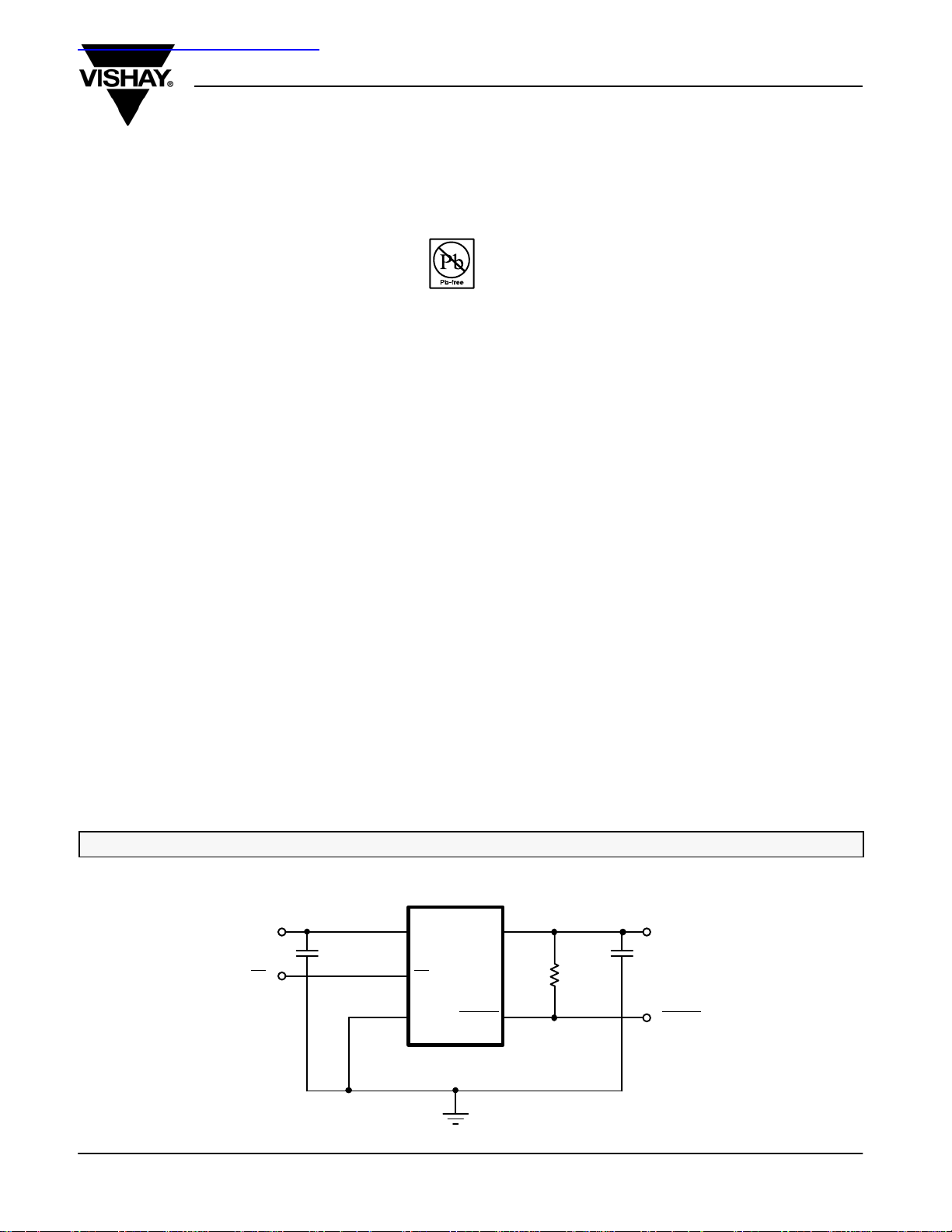
TYPICAL APPLICATION CIRCUIT
V
IN
2.2 mF
SD
Document Number: 72013
S-51147—Rev. F, 20-Jun-05
Si91872
V
IN
SD
GND
MLP33-5
V
OUT
ERROR
51 kW
V
2.2 mF
ERROR
OUT
www.vishay.com
1

Si91872
,
TA = 25_C, VIN = V
+ 1 V, I
= 1 mA
()
(V
w 2.6 V)
VIN V
OUT
mV
Dropout Voltage
d, g
()
Ground Pin Current
e, g
()
Ground Pin Current
e, g
()
Vishay Siliconix
ABSOLUTE MAXIMUM RATINGS
,
R
(qJA)
a
)
JA
STG
OUT:
Temp
a
J(max)
= 25_C
A
A
J
0.2 W.
Limits
−40 to 85_C
a
MinbTypcMaxbUnit
55_C/W. . . . . . . . . . . . . . . . . . . . . . . . . . . . . . . . . .
8_C/W. . . . . . . . . . . . . . . . . . . . . . . . . . . . . . . . . .
150_C. . . . . . . . . . . . . . . . . . . . . . .
−65_C to 150_C. . . . . . . . . . . . . . . . . . . . . . . . . .
−40_C to 85_C. . . . . . . . . . . . . . . . . . . .
−40_C to 125_C. . . . . . . . . . . . . . . . . . .
Absolute Maximum Ratings
Input Voltage, V
V
ERROR
Output Current, I
Output Voltage, V
Package Power Dissipation, (P
to GND −6.0 to 6.5 V. . . . . . . . . . . . . . . . . . . . . . . . . . . . . . .
IN
, VSD (See Detailed Description) −0.3 V to V
OUT
OUT
d
. . . . . . . . . . . . . . . . . .
b
)
Short Circuit Protected. . . . . . . . . . . . . . . . . . . . . . . . . .
IN
−0.3 V to VIN + 0.3 V. . . . . . . . . . . . . . . . . . . . . . . . . . . .
2.3 W. . . . . . . . . . . . . . . . . . . . . . . . . . . . . .
Thermal Resistance (q
Maximum Junction Temperature, T
Storage Temperature, T
Notes
a. Device mounted with all leads soldered or welded to PC board.
b. Derate 20 mW/_C above T
Stresses beyond those listed under “Absolute Maximum Ratings” may cause permanent damage to the device. These are stress ratings only, and functional operation
of the device at these or any other conditions beyond those indicated in the operational sections of the specifications is not implied. Exposure to absolute maximum rating
conditions for extended periods may affect device reliability.
RECOMMENDED OPERATING RANGE
Input Voltage, V
Input Voltage, V
IN
. . . . . . . . . . . . . . . . . . . . . . . . . . . . . . . . . . . . . . .
SD
Output Current 0 to 300 mA. . . . . . . . . . . . . . . . . . . . . . . . . . . . . . . . . . . . . . . .
a
, C
C
(Ceramic) 2.2 mF. . . . . . . . . . . . . . . . . . . . . . . . . . . . . . . . . . . . . . .
IN
OUT
2 V to 6 V. . . . . . . . . . . . . . . . . . . . . . . . . . . . . . . . . . . . . . . .
0 V to V
Operating Ambient Temperature, T
IN
Operating Junction Temperature, T
Notes
a. Maximum ESR of C
SPECIFICATIONS
Test Conditions Unless Specified
T
Parameter Symbol
= 25_C, V
CIN = 2 mF, C
= V
OUT(nom)
= 2.0 mF, VSD = 1.5 V
OUT
+ 1 V, I
OUT
= 1 mA
Input Voltage Range V
IN
Output Voltage Accuracy 1 mA v I
Line Regulation (V
Line Regulation
(3.0 V < V
OUT
v 3 V) Full −0.06 0.18
OUT
From VIN = V
v3.6 V)
DV
DV
100
OUT
V
IN
OUT(nom)
Line Regulation (5-V Version)
Dropout Voltage
OUT(nom)
Dropout Voltage
(V
OUT(nom)
Ground Pin Current
(V
OUT(nom)
Ground Pin Current
(V
OUT(nom)
Peak Output current I
Output Noise Voltage e
d, g
d, g
t 2.6 V, VIN w 2 V)
e, g
v 3 V)
e, g
u 3 V)
VIN − V
I
GND
O(peak)
OUT
V
OUT
V
N
OUT
Full 2 6 V
Room −2.0 1 2.0
Full −3.0 1 3.0
Room −2.5 1 2.5
Full −3.5 1 3.5
Full 0 0.3
v 300 mA
OUT
OUT(nom)
V
OUT
+ 1 V to V
V
w 1.8 V
OUT
= 1.2 V, 1.5 V
OUT(nom)
+ 2 V
From VIN = 5.5 V to 6 V Full 0 0.4
I
= 1 mA Room 1
OUT
I
= 50 mA
OUT
I
= 300 mA
OUT
I
= 50 mA
OUT
I
= 300 mA
OUT
I
= 0 mA
OUT
I
= 300 mA
OUT
I
= 0 mA
OUT
I
= 300 mA
OUT
w 0.95 x V
= 2.6 V, BW = 10 Hz to 100 kHz,
0 mA t I
. tPW = 2 ms Full 400 mA
OUT(nom)
t 150 mA
OUT
Room 45 80
Full 50 90
Room 300 350
Full 415
Room 65 100
Full 120
Room 400 520
Full 570
Room 100 150
Full 180
Room 130 200
Full 330
Room 11 0 170
Full 200
Room 150 225
Full 275
Room 75 mV(rms)
%
%/V
mV
mA
www.vishay.com
2
Document Number: 72013
S-51147—Rev. F, 20-Jun-05

Si91872
pp j
OUT IN
OUT
mV
C
ERROR Voltage Threshold
V
ERROR
%
Vishay Siliconix
SPECIFICATIONS
Test Conditions Unless Specified
Test Conditions Unless Specified
TA = 25_C, VIN = V
TA = 25_C, VIN = V
CIN = 2 mF, C
Parameter UnitMax
Symbol
CIN = 2 mF, C
OUT
OUT
+ 1 V, I
+ 1 V, I
OUT(nom)
OUT(nom)
= 2.0 mF, VSD = 1.5 V
= 2.0 mF, VSD = 1.5 V
OUT
OUT
= 1 mA,
= 1 mA,
Temp
Temp
a
a
Min
f = 1 kHz Room 60
Ripple Rejection DV
OUT
/DV
I
IN
= 300 mA f = 10 kHz Room 40 dB
OUT
f = 100 kHz Room 30
Dynamic Line Regulation DV
Dynamic Load Regulation DV
Thermal Shutdown Junction
Temperature
T
Thermal Hysteresis T
Reverse current I
Short Circuit Current I
O(line)
O(load)
J(S/D)
HYST
R
SC
VIN : V
I
OUT
OUT(nom)
= 2 ms, I
t
r/tf
+ 1 V to V
= 300 mA
OUT
OUT(nom)
+ 2 V
Room 20
: 1 mA to 300 mA, tr/tf = 2 ms Room 25
Room 150
Room 20
VIN = −6.0 V Room 1 mA
V
= 0 V Room 700 mA
OUT
Shutdown
Shutdown Supply Current I
SD Pin Input Voltage V
CC(off)
SD
Low = Regulator OFF (Falling) Full 0.4
Auto Discharge Resistance R_DIS Si91872 Only Room 100 W
SD Pin Input Current
SD Hysteresis V
V
Turn-On Time t
OUT
f
I
IN(SD)
HYST(SD)
ON
V
SD
VSD = 0 V Room 0.1 1 mA
High = Regulator ON (Rising) Full 1.5 V
VSD = 1.5 V, VIN = 6 V Room 0.7 mA
Full 150 mV
(See Figure 1), I
= 100 mA Room 50 ms
LOAD
ERROR Output
ERROR High Leakage I
ERROR Low Voltage V
ERROR Voltage Threshold V
ERROR Voltage Threshold
Hysteresis
Notes
a. Room = 25_C, Full = −40 to 85_C.
b. The algebraic convention whereby the most negative value is a minimum and the most positive a maximum.
c. Typical values are for DESIGN AID ONLY, not guaranteed nor subject to production testing.
d. Dropout voltage is defined as the input to output differential voltage at which the output voltage drops 2% below the output voltage measured with a 1-V
differential, provided that V
e. Ground current is specified for normal operation as well as “drop-out” operation.
f. The device’s shutdown pin includes a typical 2-MW internal pull-down resistor connected to ground.
g. V
OUT(nom)
is V
when measured with a 1-V differential to VIN.
OUT
does not not drop below 2.0 V.
IN
OFF
OL
ERROR
V
HYST(ERROR)
ERROR v VIN. V
V
OUT
V
Falling, I
OUT
V
OUT(nom)
in Regulation Full 1 mA
OUT
I
= 0.5 mA Full 0.4 V
SINK
Below V
OUT
g
g
OUT(nom)
= 1 mA, V
, VIN w 2 V
OUT(nom)
w 2 V
Full −2 −4 −6
t 2 V, VIN u 2 V Full −4
Room 1.5
Limits
−40 to 85_C
b
Typ
c
b
IN
mV
_C
V
%
TIMING WAVEFORMS
Document Number: 72013
S-51147—Rev. F, 20-Jun-05
0.95 V
tr v 1 mS
t
ON
NOM
0 V
V
SD
V
OUT
FIGURE 1. Timing Diagram for Power-Up
V
V
IN
NOM
www.vishay.com
3

Si91872
Vishay Siliconix
PIN CONFIGURATION: MLP33-5
MLP33-5 PowerPAK
SD
ERROR
V
V
OUT
1
2
3
IN
4
Top View
5
GND
GND
5
GND
GND
PIN DESCRIPTION
Pin Number Name Function
1 SD By applying less than 0.4 V to this pin, the device will be turned off. Connect this pin to VIN if unused
2 ERROR The open drain output is an error flag output which goes low when V
3 V
4 V
5 GND Ground pin. For better thermal capability, directly connected to large ground plane
IN
OUT
Input supply pin. Bypass this pin with a 1-mF ceramic or tantalum capacitor to ground
Output voltage. Connect C
between this pin and ground.
OUT
drops 4% below its nominal voltage.
OUT
ORDERING INFORMATION
Standard
Part Number
Si91872DMP-12-T1 Si91872DMP-12-E3 7212 1.2
Si91872DMP-18-T1 Si91872DMP-18-E3 7218 1.8
Si91872DMP-25-T1 Si91872DMP-25-E3 7225 2.5
Si91872DMP-26-T1 Si91872DMP-26-E3 7226 2.6
Si91872DMP-28-T1 Si91872DMP-28-E3 7228 2.8
Si91872DMP-30-T1 Si91872DMP-30-E3 7230 3.0
Si91872DMP-33-T1 Si91872DMP-33-E3 7233 3.3
Si91872DMP-50-T1 Si91872DMP-50-E3 7250 5.0
Lead (Pb)-Free
Part Number
Marking Voltage
Temp.
Range
_
−40 to 85_C MLP33-5
1
2
3
4
Bottom View
Pkg.
www.vishay.com
4
Document Number: 72013
S-51147—Rev. F, 20-Jun-05

Vishay Siliconix
TYPICAL CHARACTERISTICS (INTERNALLY REGULATED, 25_C UNLESS NOTED)
Si91872
0.30
0.15
0.00
−0.15
−0.30
Output Voltage (%)
−0.45
−0.60
−0.75
150
125
mA)
(I
100
GND
75
Normalized Output Voltage vs. Load Current
VIN = V
0 50 100 150 200 250 300
+ 1 V
OUT(nom)
Load Current (mA)
GND Current vs. Load Current
V
= 3.0 V
V
OUT
IN
= 4.0 V
85_C
25_C
−40_C
0.4
Normalized V
VIN = V
0.2
−0.0
(%)V
−0.2
OUT
−0.4
−0.6
−0.8
−1.0
−40 −15 10 35 60 85
OUT(nom)
Ambient Temperature (_C)
vs. Temperature
OUT
+ 1 V
I
= 0 mA
OUT
I
OUT
= 300 mA
No Load GND Pin Current vs. Input Voltage
300
250
200
mA)
(I
150
GND
100
50
I
OUT
I
OUT
= 75 mA
= 150 mA
85_C
25_C
−40_C
50
0 50 100 150 200 250 300
0
CIN = 1 mF
C
= 1 mF
OUT
I
= 150 mA
LOAD
V
−20
−40
Gain (dB)
−60
−80
10 100 1000 10000 100000 1000000
Document Number: 72013
S-51147—Rev. F, 20-Jun-05
OUT
= 3.0 V
Load Current (mA)
Power Supply Rejection
Frequency (Hz)
0
234567
Input Voltage (V)
Output Short Circuit Current vs. Temperature
750
725
700
(mA)I
675
SC
650
625
600
−40 −15 10 35 60 85
AmbientTemperature (_C)
V
= 2.6 V
OUT
www.vishay.com
5

Si91872
Vishay Siliconix
TYPICAL CHARACTERISTICS (INTERNALLY REGULATED, 25_C UNLESS NOTED)
350
V
= 3.0 V
OUT
50
0
0 60 120 180 240 300
I
LOAD (mA)
(mV)V
DROP
300
250
200
150
100
Dropout Voltage vs. Temperature
350
V
= 3.0 V
OUT
Dropout Voltage vs. Load Current
300
250
200
(mV)V
150
DROP
100
50
0
−50 −25 0 25 50 75 100 125 150
I
= 300 mA
OUT
I
= 150 mA
OUT
I
= 75 mA
OUT
Junction Temperature (_C)
I
OUT
I
OUT
= 10 mA
= 0 mA
3.0
VIN − V
V
= 3.0 V
OUT
2.5
2.0
(V)V
1.5
OUT
1.0
0.5
0.0
0123456
400
350
300
250
200
150
I
Dropout Voltage (mV)
100
50
0
1.0 1.5 2.0 2.5 3.0 3.5 4.0 4.5 5.0
OUT
= 75 mA
Transfer Characteristic
OUT
VIN (V)
Dropout Voltage vs. V
I
= 300 mA
OUT
I
I
= 10 mA
OUT
V
OUT
OUT
OUT
= 150 mA
www.vishay.com
6
Document Number: 72013
S-51147—Rev. F, 20-Jun-05

TYPICAL WAVEFORMS
Si91872
Vishay Siliconix
V
OUT
10 mV/div
I
LOAD
100 mA/div
20 ms/div
Load Transient Response-1
V
= 3.0 V
OUT
C
= 1 mF
OUT
I
= 1 to 150 mA
LOAD
t
= 2 msec
rise
V
OUT
10 mV/div
I
LOAD
100 mA/div
20 ms/div
Load Transient Response-2
V
= 3.0 V
OUT
C
= 1 mF
OUT
I
= 150 to 1 mA
LOAD
t
= 2 msec
fall
LineTransient Response-1
V
OUT
10 mV/div
V
IN
2 V/div
20 ms/div
Document Number: 72013
S-51147—Rev. F, 20-Jun-05
V
INSTEP
V
OUT
C
OUT
C
IN
I
LOAD
t
rise
= 4 to 5 V
= 3 V
= 1 mF
= 1 mF
= 150 mA
= 5 msec
V
OUT
10 mV/div
V
2 V/div
IN
20 ms/div
LineTransient Respons-2
V
= 5 to 4 V
INSTEP
V
= 3 V
OUT
C
= 1 mF
OUT
C
= 1 mF
IN
I
= 150 mA
LOAD
t
= 5 msec
fall
www.vishay.com
7

Si91872
Vishay Siliconix
TYPICAL WAVEFORMS
Output Noise
V
OUT
200 mV/div
4 ms/div 10 Hz
V
= 4 V
IN
V
= 3 V
OUT
I
= 150 mA
OUT
BW = 10 Hz to 100 kHz
FUNCTIONAL BLOCK DIAGRAM
10
Ǹ
mVń Hz
Output Spectral Noise Density
0.01
Noise Spectrum
V
= 4 V
IN
V
= 3 V
OUT
I
= 150 mA
LOAD
1 MHz
www.vishay.com
8
V
SD
Si91872
IN
Reverse Polarity
Protection
Reference
Thermal
Sensor
Current
Shutdown
Control
Limit
−
+
V
OUT
ERROR
GND
Document Number: 72013
S-51147—Rev. F, 20-Jun-05

DETAILED DESCRIPTION
Si91872
Vishay Siliconix
The Si91872 is a low-noise, low drop-out and low quiescent
current linear voltage regulator, packaged in a small footprint
MLP33-5 package. The Si91872 can supply loads up to
300 mA. As shown in the block diagram, the circuit consists of
a bandgap reference, error amplifier, p-channel pass transistor
and feedback resistor string. Additional blocks, not shown in
the block diagram, include a precise current limiter, reverse
battery and current protection, and thermal sensor.
Thermal Overload Protection
The thermal overload protection limits the total power
dissipation and protects the device from being damaged.
When the junction temperature exceeds 150_C, the device
turns the p-channel pass transistor off.
Reverse Battery Protection
The Si91872 has a battery reverse protection circuitry that
disconnects the internal circuitry when V
drops below the
IN
GND voltage. There is no current drawn in such an event.
When the SD pin is hardwired to VIN, the user must connect
pin to VIN via a 100-kW resistor if reverse battery
the SD
protection is desired. Hardwiring the SD
pin directly to the V
pin is allowed when reverse battery protection is not desired.
ERROR
ERROR is an open drain output that goes low when V
OUT
is
less than 4% of its normal value. To obtain a logic level output,
connect a pull-up resister from ERROR to V
voltage equal to or less than V
impedance (off) when SD
pin is low.
. ERROR pin is high
IN
or any other
OUT
package and the circuit board, and the ambient temperature.
The power dissipation is defined as
= (VIN – V
P
D
OUT
) * I
OUT
.
Junction temperature is defined as
T
= TA + ((PD * (RθJC + RθCA)).
J
To calculate the limits of performance, these equations must
be rewritten.
Allowable power dissipation is calculated using the equation
P
= (TJ − T
D
)/ (RθJC + RθCA)
A
While allowable output current is calculated using the equation
I
OUT
= (TJ − T
)/ (RθJC + RθCA) * (VIN – V
A
OUT
).
Ratings of the Si91872 that must be observed are
T
= 125 _C, T
Jmax
IN
Rθ
= 8 _C/W.
JC
= 85 _C, (VIN – V
Amax
OUT)max
= 5.3 V,
The value of RθCA is dependent on the PC board used. The
value of Rθ
for the board used in device characterization is
CA
approximately 46 _C/W.
Figure 1 shows the performance limits graphically for the
Si91872 mounted on the circuit board used for thermal
characterization.
Auto-Discharge
has an internal 100-W (typ.) discharge path to ground
V
OUT
when SD
pin is low for the Si91872.
Stability
0.35
0.30
0.25
TA = 50_C
TA = 70_C
The circuit is stable with only a small output capacitor equal to
0.20
6 nF/mA (= 2 mF @ 300 mA). Since the bandwidth of the error
amplifier is around 1−3 MHz and the dominant pole is at the
output node, the capacitor should be capacitive in this range,
(A)I
OUT
TA = 85_C
0.15
i.e., for 150-mA load current, an ESR <0.2 W is necessary.
Parasitic inductance of about 10 nH can be tolerated.
Safe Operating Area
The ability of the Si91872 to supply current is ultimately
dependent on the junction temperature of the pass device.
Junction temperature is in turn dependent on power
dissipation in the pass device, the thermal resistance of the
Vishay Siliconix maintains worldwide manufacturing capability. Products may be manufactured at one of several qualified locations. Reliability da ta for Silicon Technology and
Package Reliability represent a composite of all qualified locations. For related documents such as package/tape drawings, part marking, and reliability data, see
http://www.vishay.com/ppg?72013
Document Number: 72013
S-51147—Rev. F, 20-Jun-05
.
0.10
0.05
(VIN − V
0.00
0123456
Figure 1. Safe Operating Area
OUT)MAX
VIN − V
= 5.3 V
OUT
(V)
www.vishay.com
9

Copyright © Each Manufacturing Company.
All Datasheets cannot be modified without permission.
This datasheet has been download from :
www.AllDataSheet.com
100% Free DataSheet Search Site.
Free Download.
No Register.
Fast Search System.
www.AllDataSheet.com
 Loading...