

Datasheet Si9183DT-18-T1, Si9183DT-25-T1, Si9183DT-285-T1, Si9183DT-28-T1, Si9183DT-30-T1 Datasheet (Vishay) [ru]
...
Vishay Siliconix
High-Performance, Size Saving 150-mA CMOS LDO Regulator
FEATURES
Si9183
D Low 135-mV Dropout at 150-mA Load
D Guaranteed 150-mA Output Current
D 300-mA Peak Output Current Capability
Available
D Uses Low ESR Ceramic Output Capacitor
D Fast Load And Line Transient Response
D Low Output Noise
D 1-mA Maximum Shutdown Current
D Built-in Short Circuit And Thermal Protection
D Fixed 1.8-V, 2.5-V, 2.8-V, 2.85-V, 3.0-V, 3.3-V, 5.0-V
or Adjustable Output Voltage Options (Version B)
DESCRIPTION
The Si9183 is a high performance yet size saving 150-mA
CMOS LDO (low dropout) voltage regulator. Its ultra low
ground current and dropout voltage prolong battery life in
portable electronics. The device provides LINE/LOAD
transient response and ripple rejection superior to that of
Bipolar or BiCMOS LDO regulators. It is designed to maintain
regulation while delivering 300-mA peak current. The Si9183
drives lower cost ceramic, as well as tantalum, output
capacitors. Stability is guaranteed from maximum load current
down to 0-mA load. An external noise bypass capacitor
connected to the device’s CBP pin will reduce the LDO’s
D Thin SOT-23 5-Pin Package
APPLICATIONS
D Battery Powered Portable Systems
D Cellular Phones
D PDAs, Palmtops
D Pagers
D Post Regulators for Multi-Output Converters
D Notebook Computers
self-noise for low noise applications. The Si9183 includes a
shutdown feature that allows users to completely disable the
device and save power when no output is required.
The Si9183, in Thin SOT23-5 packaging, is available in two
versions (Version A or B). Version A offers low noise
performance, while Version B features adjustable output
voltage.
The Si9183 is available in both standard and lead (Pb)-free
packages.
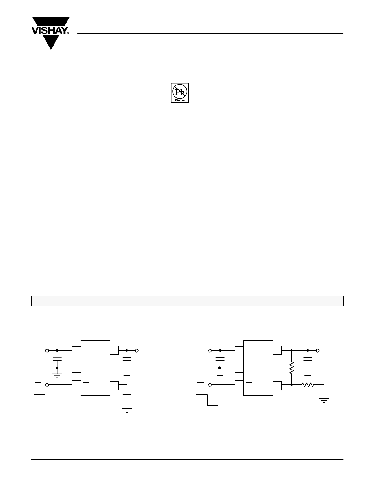
TYPICAL APPLICATIONS CIRCUITS
Si9183-A
1
V
IN
1 mF 2.2 mF
SD
ON
OFF
FIGURE 1. Version A with Low Output Noise FIGURE 2. Version B with Adjustable Output
Document Number: 71258
S-51147—Rev. G, 20-Jun-05
V
IN
2
GND
3
SD
Thin SOT-23, 5-Lead
5
V
OUT
4
BP
V
0.1 mF
OUT
Si9183-B
1
V
IN
1 mF 2.2 mF
SD
ON
OFF
V
IN
2
GND
3
SD
Thin SOT-23, 5-Lead
5
V
OUT
4
FB
V
OUT
www.vishay.com
1
Si9183
Output Voltage Accuracy
OUT
DV
100
VIN V
%/V
@
)
@V
w 2.5 V)
IN OUT
Dropout Voltage
d
GND
m
BW = 50 Hz to 100 kHz
Vishay Siliconix
ABSOLUTE MAXIMUM RATINGS
Input Voltage, V
Input Voltage, V
SD
Output Current, I
Output Voltage, V
Maximum Junction Temperature, T
Storage Temperature, T
IN
. . . . . . . . . . . . . . . . . . . . . . . . . . . . . . . . .
SD
OUT
OUT
STG
150_C. . . . . . . . . . . . . . . . . . . . . . .
J(max)
Short Circuit Protected. . . . . . . . . . . . . . . . . . . . . . . . . .
−0.3 V to V
−65_C to 125_C. . . . . . . . . . . . . . . . . . . . . . . . . .
ESD (Human Body Model) 2 kV. . . . . . . . . . . . . . . . . . . . . . . . . . . . . . . . . . . . .
−0.3 V to V
+ 0.3 V. . . . . . . . . . . . . . . . . . . . . . . .
O(nom)
6.5 V. . . . . . . . . . . . . . . . . . . . . . . . . . . . . . . . . . . . . . . . . . . .
IN
Power Dissipation (Package)
5-Pin SOT-23 555 mW. . . . . . . . . . . . . . . . . . . . . . . . . . . . . . . . . . . . . . . . . . . .
Thermal Impedance (Q
5-Pin SOT-23 180 _C/W. . . . . . . . . . . . . . . . . . . . . . . . . . . . . . . . . . . . . . . . . . .
Notes
a. Device mounted with all leads soldered or welded to multi-layer (1S2P)
JEDEC board, horizontal orientation.
b. Derate 5.5 mW/_C above T
Stresses beyond those listed under “Absolute Maximum Ratings” may cause permanent damage to the device. These are stress ratings only, and functional operation
of the device at these or any other conditions beyond those indicated in the operational sections of the specifications is not implied. Exposure to absolute maximum rating
conditions for extended periods may affect device reliability.
RECOMMENDED OPERATING RANGE
Input Voltage, V
Output Voltage, V
SD
Input Voltage, V
= 1 mF, C
C
IN
C
Range = 1 mF to 10 mF ("20% tolerance, "20% over temperature; ESR = 0.4 to 4 W at dc to 100 kHz, 0 t0 0.4 W > 100 kHz) )
OUT
IN
(Adjustable Version) 1.5 V to 5 V. . . . . . . . . . . . . . . . . .
OUT
. . . . . . . . . . . . . . . . . . . . . . . . . . . . . . . . . . . .
SD
= 2.2 mF (ceramic, X5R or X7R type) , CBP = 0.1 mF (ceramic)
OUT
2 V to 6 V. . . . . . . . . . . . . . . . . . . . . . . . . . . . . . . . . . . . . . . .
0 V to V
Operating Ambient Temperature, T
Operating Junction Temperature, T
IN
a
, b
)
JA
= 25_C.
A
A
J
−40_C to 85_C. . . . . . . . . . . . . . . . . . . .
−40_C to 125_C. . . . . . . . . . . . . . . . . . .
SPECIFICATIONS (TA = 25_C)
Test Conditions
Unless Otherwise Specified
VIN = V
C
Parameter Symbol
Input Voltage Range V
IN
= 1 mF, C
IN
Output Voltage Range Adjustable Version Full 1.5 5
V
V
OUT
OUT
V
VIN − V
VIN − V
GND
IN(off)
O(peak)
FB
OUT(nom)
OUT
OUT
FB
N
1 mA v I
From VIN = V
From VIN = 5.5 V to 6 V Full −0.18 0.18
V
= 1.5 V, From VIN = 2.5 V to 3.5 V Full −0.18 0.18
OUT
V
= 5 V, From VIN = 5.5 V to 6 V Full −0.18 0.18
OUT
V
w 0.95 x V
OUT
BW = 50 Hz to 100 kHz
I
= 150 mA
OUT
Output Voltage Accuracy
(Fixed Versions)
Feedback Voltage (ADJ version) V
Line Regulation
(Except 5-V Version)
Line Regulation (5-V Version)
Line Regulation (ADJ Version)
Dropout Voltage
V
OUT
Dropout Voltage
(@V
OUT
d
w 2.5 V
d
t 2.5 V, VIN w 2 V)
Ground Pin Current I
Shutdown Supply Current I
FB Pin Current I
Peak Output Current I
Output Noise Voltage e
+ 1 V, I
OUT(nom)
= 2.2 mF, VSD = 1.5 V
OUT
OUT
= 1 mA
TempaMinbTypcMax
Full 2 6
v 150 mA
OUT
Room −1.5 1.5
Full −2.5 2.5
Room 1.188 1.215 1.240
Full 1.176 1.252
+ 1 V
OUT(nom)
to V
I
I
OUT
I
OUT
I
OUT
+ 2 V
OUT(nom)
= 10 mA Room 1 20
OUT
= 150 mA
= 150 mA
I
= 0 mA Room 150
OUT
= 150 mA
Full −0.18 0.18
Room 135 170
Full 180 220
Room 235 320
Full 380
Room 500
Full 900
VSD = 0 V Full 0.1 1 mA
VFB = 1.2 V Room 2 100 nA
, tpw = 2 ms Room 250 300 mA
OUT(nom)
w/o C
BP
Room 300
CBP = 0.1 mF Room 100
Limits
−40 to 85_C
b
Unit
V
% V
O(nom)
V
%/V
mV
mA
mV (rms)
www.vishay.com
2
Document Number: 71258
S-51147—Rev. G, 20-Jun-05
Si9183
pp j
OUT IN
OUT
mV
VIN = 4.3 V
Vishay Siliconix
SPECIFICATIONS (TA = 25_C)
Test Conditions
Test Conditions
Unless Otherwise Specified
Unless Otherwise Specified
VIN = V
VIN = V
C
C
= 1 mF, C
Parameter UnitMax
Symbol
= 1 mF, C
IN
IN
+ 1 V, I
+ 1 V, I
OUT(nom)
OUT(nom)
= 2.2 mF, VSD = 1.5 V
= 2.2 mF, VSD = 1.5 V
OUT
OUT
OUT
OUT
= 1 mA
= 1 mA
Temp
a
Min
f = 1 kHz Room 60
Ripple Rejection DV
OUT
/DV
I
IN
OUT
= 150 mA
f = 10 kHz Room 40
f = 100 kHz Room 30
Dynamic Line Regulation DV
Dynamic Load Regulation DV
V
Turn-On-Time t
OUT
O(line)
O(load)
ON
VIN : V
I
OUT
V
VIN = 4.3 V
OUT
OUT(nom)
t
= 5 ms, I
R/tF
+ 1 V to V
OUT
= 150 mA
OUT(nom)
+ 2 V
Room 10
: 1 mA to 150 mA, tR/tF = 2 ms Room 30
w/o CBP Cap Room 5
= 3.3 V
CBP = 0.1 mF Room 1000
Thermal Shutdown
Thermal Shutdown Junction Temp t
Thermal Hysteresis t
Short Circuit Current I
J(s/d)
HYST
SC
V
= 0 V Room 400 mA
OUT
Room 165
Room 20
Shutdown Input
V
SD Input Voltage
SD Input Current
e
Shutdown Hysteresis V
Notes
a. Room = 25_C, Full = −40 to 85_C.
b. The algebraic convention whereby the most negative value is a minimum and the most positive a maximum.
c. Typical values are for DESIGN AID ONLY, not guaranteed nor subject to production testing. Typical values for dropout voltage at V
V
= 2.5 V, while typical values for dropout voltage at V
OUT
d. Dropout voltage is defined as the input to output differential voltage at which the output voltage drops 2% below the output voltage measured with a 1-V
differential, provided that V
e. The device’s shutdown pin includes a typical 6-MW internal pull-down resistor connected to ground.
f. V
is defined as the output voltage of the DUT at 1 mA.
OUT
does not not drop below 2.0 V.
IN
IH
V
IL
I
IL
I
IH
HYST
High = Regulator ON (Rising) Full 1.2 V
Low = Regulator OFF (Falling) Full 0.4
VSD = 0 V, Regulator OFF Room 0.01
VSD = 6 V, Regulator ON Room 1.0
Full 100 mV
< 2 V are measured at V
OUT
OUT
= 1.8 V.
Limits
−40 to 85_C
b
Typ
c
OUT
b
IN
w 2 V are measured at
dB
mV
ms
_
_C
V
mA
Document Number: 71258
S-51147—Rev. G, 20-Jun-05
www.vishay.com
3
Si9183
Vishay Siliconix
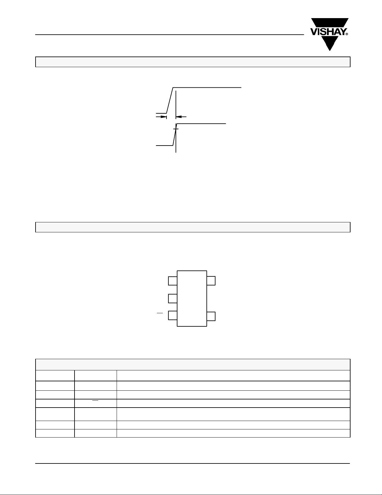
TIMING WAVEFORMS
V
IN
t
ON
0.95 V
NOM
V
OUTVOUT
FIGURE 3. Timing Diagram for Power-Up
V
NOM
PIN CONFIGURATION
Thin SOT-23, 5-Pin
V
GND
SD
1
IN
2
3
5
V
OUT
BP (Version A)
4
FB (Version B)
PIN DESCRIPTION
Pin Number Name Function
1 V
2 GND Ground pin. Local ground for CBP and C
3 SD By applying less than 0.4 V to this pin, the device will be turned off. Connect this pin to VIN if unused.
4 (Version A) BP
4 (Version B) FB Connect to divided output voltage to adjust the regulation point.
5 V
IN
OUT
Input supply pin. Bypass this pin with a 1-mF ceramic or tantalum capacitor to ground.
.
OUT
Noise bypass pin. For low noise applications, a 0.1-mF or larger ceramic capacitor should be connected from this pin to
ground.
Output voltage. Connect C
between this pin and ground.
OUT
www.vishay.com
4
Document Number: 71258
S-51147—Rev. G, 20-Jun-05

Vishay Siliconix
Thin
ORDERING INFORMATION
Lead (Pb)-Free
Part Number
Si9183DT-18-T1 Si9183DT-18-T1—E3 A2LL 1.8 V
Si9183DT-25-T1 Si9183DT-25-T1—E3 A4LL 2.5 V
Si9183DT-28-T1 Si9183DT-28-T1—E3 A5LL 2.8 V
Si9183DT-285-T1 Si9183DT-285-T1—E3 B3LL 2.85 V
Si9183DT-30-T1 Si9183DT-30-T1—E3 A6LL 3.0 V
Si9183DT-33-T1 Si9183DT-33-T1—E3 A7LL 3.3 V
Si9183DT-50-T1 Si9183DT-50-T1—E3 A8LL 5.0 V
Si9183DT-AD-T1 Si9183DT-AD-T1—E3 A9LL Adjustable
NOTE: LL = Lot Code
TYPICAL CHARACTERISTICS (INTERNALLY REGULATED, 25_C UNLESS NOTED)
Dropout Voltage vs. Load Current
V
= 2.5 V
OUT
(mV)V
DROP
300
250
200
150
100
Part Number
Marking Voltage Temperature Range Package
_
−40 to 85_C
Eval Kit Temperature Range Board Type
Si9183DB −40 to 85_C Surface Mount
(V)V
OUT
2.5
2.0
1.5
1.0
R
LOAD
VIN − V
= 250 W
Transfer Characteristic
OUT
R
LOAD
Thin
SOT23-5
= 16.6 W
Si9183
50
0
0 60 120 180 240 300
I
LOAD (mA)
Dropout Voltage vs. Temperature
375
350
V
= 2.5 V
OUT
325
300
275
250
225
(mV)V
200
175
DROP
150
125
100
75
50
25
0
−50 −25 0 25 50 75 100 125 150
Junction Temperature (_C)
I
OUT
I
OUT
I
OUT
I
OUT
I
OUT
= 300 mA
= 150 mA
= 75 mA
= 10 mA
= 0 mA
0.5
0.0
0123456
VIN (V)
500
Dropout Voltage vs. V
400
300
200
I
= 150 mA
Dropout Voltage (mV)
I
= 75 mA
OUT
100
I
= 10 mA
OUT
0
1.0 1.5 2.0 2.5 3.0 3.5 4.0 4.5 5.0
OUT
V
OUT
I
OUT
OUT
= 300 mA
Document Number: 71258
S-51147—Rev. G, 20-Jun-05
www.vishay.com
5

Si9183
Vishay Siliconix
TYPICAL CHARACTERISTICS (INTERNALLY REGULATED, 25_C UNLESS NOTED)
0.30
0.15
0.00
−0.15
−0.30
Output Voltage (%)
−0.45
−0.60
−0.75
500
400
300
mA)
(I
GND
200
Normalized Output Voltage vs. Load Current
VIN = V
0 25 50 75 100 125 150
OUT(nom)
+ 1 V
Load Current (mA)
GND Current vs. Load Current
V
= 2.5 V
OUT
V
= 3.5 V
IN
85_C
−40_C
−0.0
Normalized V
−0.2
−0.4
I
= 150 mA
(%)V
−0.6
OUT
−0.8
−1.0
−1.2
−40 −15 10 35 60 85
OUT
VIN = V
OUT(nom)
Ambient Temperature (_C)
OUT
+ 1 V
vs. Temperature
I
= 0 mA
OUT
No Load GND Pin Current vs. Input Voltage
300
250
200
mA)
(I
GND
150
100
85_C
I
OUT
= 75 mA
−40_C
100
0
1.5
1.4
1.3
1.2
1.1
IH
I
1.0
0.9
0.8
0.7
0.6
0.5
−40 −15 10 35 60 85
www.vishay.com
6
0 25 50 75 100 125 150
Load Current (mA)
Shutdown Pin Input Current vs. Temperature
V
= 2.5 V
OUT
V
= 6.5 V
SD
Ambient Temperature
50
0
23456
Input Voltage (V)
Shutdown Threshold vs. Temperature
V
= 2.5 V
OUT
V
IH
V
IL
−40 −15 10 35 60 85
Ambient Temperature
Document Number: 71258
S-51147—Rev. G, 20-Jun-05
(V)V
, V
1.5
1.4
1.3
1.2
1.1
1.0
IH
0.9
IL
0.8
0.7
0.6
0.5
0.4

Vishay Siliconix
TYPICAL CHARACTERISTICS (INTERNALLY REGULATED, 25_C UNLESS NOTED)
Si9183
0.75
V
= 2.5 V
OUT
0.65
0.55
(A)I
SC
0.45
0.35
0.25
−40 −15 10 35 60 85
Ambient Temperature
TYPICAL WAVEFORMS
Turn-On Delay
SD 2 V/div
ISC vs. Temperature
−20
−40
Gain (dB)
−60
−80
SD 2 V/div
0
10
Power Supply Rejection
CIN = 1 mF
C
= 2.2 mF
OUT
I
= 150 mA
LOAD
100 1 K 10 K 100 K 1 M
Frequency (Hz)
Turn-Off Delay
V
2 V/div
OUT
V
2 V/div
OUT
10.00 ms/div 5.00 ms/div
V
= 4.2 V
IN
V
= 3.3 V
OUT
C
= 0.1 mF
BP
I
= 350 mA
LOAD
Output Noise
V
= 4.2 V
IN
V
= 3.3 V
OUT
C
= 0.1 mF
BP
I
= 350 mA
LOAD
Noise Spectrum
10.0
100 mV/div
Ǹ
mVń Hz
0.01
1 ms/div
V
= 4 V
IN
V
= 3 V
OUT
I
= 150 mA
OUT
C
= 1 mF
IN
C
= 2.2 mF
OUT
C
= 0.1 mF
BP
BW = 10 Hz to 1 MHz
100 Hz
VIN = 4 V
V
= 3
OUT
I
= 150 mA
OUT
C
= 1 mF
IN
C
= 2.2 mF
OUT
C
= 0.1 mF
BP
1 MHz
Document Number: 71258
S-51147—Rev. G, 20-Jun-05
www.vishay.com
7

Si9183
Vishay Siliconix
TYPICAL WAVEFORMS
Load Transient Response-1 Load Transient Response-2
V
OUT
10 mV/div
I
LOAD
100 mA/div
V
OUT
10 mV/div
I
LOAD
100 mA/div
V
OUT
10 mV/div
I
LOAD
100 mA/div
V
IN
1 V/div
V
= 3.0 V
OUT
C
= 2.2 mF
OUT
I
= 1 to 150 mA
LOAD
t
= 2 msec
rise
M 5.00 ms M 5.00 ms
V
= 3.0 V
OUT
C
= 2.2 mF
OUT
I
= 150 to 1 mA
LOAD
t
= 2 msec
fall
Load Transient Response-3 Load Transient Response-4
V
OUT
10 mV/div
I
LOAD
100 mA/div
V
= 3.0 V
OUT
C
= 1.0 mF
OUT
I
= 1 to 150 mA
LOAD
t
= 2 msec
rise
M 5.00 ms M 5.00 ms
V
= 3.0 V
OUT
C
= 1.0 mF
OUT
I
= 150 to 1 mA
LOAD
t
= 2 msec
fall
Line Transient Response-1 Line Transient Response-2
V
IN
1 V/div
V
OUT
10 mV/div
www.vishay.com
8
V
OUT
I
LOAD
V
= 4 to 5 V
IN
C
OUT
t
= 5 msec
rise
= 3.0 V
= 150 mA
= 2.2 mF
V
OUT
10 mV/div
M 20.0 ms M 20.0 ms
V
= 3.0 V
OUT
I
= 150 mA
LOAD
V
= 5 to 4 V
IN
C
= 2.2 mF
OUT
t
= 5 msec
fall
Document Number: 71258
S-51147—Rev. G, 20-Jun-05

BLOCK DIAGRAMS
Si9183
Vishay Siliconix
V
IN
SD
ON
C
1.0 mF
GND
IN
OFF
4BP
1
3
RFB2
6 MW
RFB1
2
+
−
+
1.215 V
V
REF
−
Switches shown for device in normal operating mode (SD = HIGH)
5
C
OUT
2.2 mF
V
OUT
FIGURE 4. 150-mA CMOS LDO Regulator (Fixed Output)
C
IN
GND
1
3
OFF
2
V
IN
1.0 mF
SD
ON
Document Number: 71258
S-51147—Rev. G, 20-Jun-05
4
6 MW
FB
+
−
+
1.215 V
V
REF
−
FIGURE 5. 150-mA CMOS LDO Regulator (Adjustable Output)
5
C
OUT
2.2 mF
R
2
V
FB
R
1
V
OUT
www.vishay.com
9

Si9183
Vishay Siliconix
DETAILED DESCRIPTION
The Si9183 is a low drop out, low quiescent current, linear
regulator family with very fast transient response. It is primarily
designed for battery powered applications where battery run
time is at a premium. The low quiescent current allows
extended standby time while low drop out voltage enables the
system to fully utilize battery power before recharge. The
Si9183 is a very fast regulator with bandwidth exceeding
50 kHz while maintaining low quiescent current at light load
conditions. With this bandwidth, the Si9183 is one of the
fastest LDO available today. The Si9183 is stable with one of
any output capacitor types from 1 mF to 10.0 mF. However,
X5R or X7R ceramic capacitors are recommended for best
output noise and transient performance.
V
IN
VIN is the input supply pin. The bypass capacitor for this pin
is not critical as long as the input supply has low enough source
impedance. For practical circuits, a 1.0-mF or larger ceramic
capacitor is recommended. When the source impedance is
not low enough and/or the source is several inches from the
Si9183, then a larger input bypass capacitor is needed. It is
required that the equivalent impedance (source impedance,
wire, and trace impedance in parallel with input bypass
capacitor impedance) must be smaller than the input
impedance of the Si9183 for stable operation. When the
source impedance, wire, and trace impedance are unknown,
it is recommended that an input bypass capacitor be used of
a value that is equal to or greater than the output capacitor.
V
OUT
GND
Ground is the common ground connection for V
It is also the local ground connection for C
BP
and V
IN
OUT
, ADJ, and SD.
ADJ
For the adjustable output version, use a resistor divider R1 and
R2, connect R1 from V
to ADJ and R2 from ADJ to ground.
OUT
R2 should be in the 25-kW to 150-kW range for low power
consumption, while maintaining adequate noise immunity.
The formula below calculates the value of R1, given the
desired output voltage and the R2 value,
ǒ
V
R1 +
OUT
V
is nominally 1.215 V.
ADJ
* V
V
ADJ
ADJ
Ǔ
R2
(1)
SHUTDOWN (SD)
controls the turning on and off of the Si9183. V
SD
guaranteed to be on when the SD
greater than 1.2 V. V
is guaranteed to be off when theSD
OUT
pin voltage equals or is
OUT
is
pin voltage equals or is less than 0.4 V. During shutdown
mode, the Si9183 will draw less than 1-mA current from the
source. To automatically turn on V
applied, tie the SD
pin to VIN.
whenever the input is
OUT
.
V
is the output voltage of the regulator. Connect a bypass
OUT
capacitor from V
to ground. The output capacitor can be
OUT
any value from 1.0 mF to 10.0 mF. A ceramic capacitor with
X5R or X7R dielectric type is recommended for best output
noise, line transient, and load transient performance.
Vishay Siliconix maintains worldwide manufacturing capability. Products may be manufactured at one of several qualified locations. Reliability data for Silicon Technology and
Package Reliability represent a composite of all qualified locations. For related documents such as package/tape drawings, part marking, and reliability data, see
http://www.vishay.com/ppg?71258
www.vishay.com
10
.
C
BP
For low noise application, connect a high frequency ceramic
capacitor from C
to ground. A 0.01-mF or a 0.1-mF X5R or
BP
X7R is recommended.
Document Number: 71258
S-51147—Rev. G, 20-Jun-05

 Loading...