

Datasheet Si9182DH-12-T1, Si9182DH-15-T1, Si9182DH-18-T1, Si9182DH-25-T1, Si9182DH-28-T1 Datasheet (Vishay) [ru]
...
Micropower 250-mA CMOS LDO Regulator
With Error Flag/Power-On-Reset
FEATURES
D Low 105-mV Dropout at 250-mA Load
D Guaranteed 250-mA Output Current
D 500-mA Peak Output Current Capability
D Uses Low ESR Ceramic Output Capacitor
D Fast Load and Line Transient Response
D Only 100-mV(rms) Noise With Noise Bypass
Capacitor
D 1-mA Maximum Shutdown Current
D Built-in Short Circuit and Thermal Protection
D Out-Of-Regulation Error Flag (Power Good or POR)
DESCRIPTION
Available
Si9182
Vishay Siliconix
D Fixed 1.215-V, 1.5-V, 1.8-V, 2.5-V, 2.8-V, 2.9-V,
3.0-V, 3.3-V, 5.0-V, or Adjustable Output Voltage
Options
D Other Output Voltages Available by Special Order
APPLICATIONS
D Cellular Phones
D Laptop and Palm Computers
D PDA, Digital Still Cameras
The Si9182 is a 250-mA CMOS LDO (low dropout) voltage
regulator. The device features ultra low ground current and
dropout voltage to prolong battery life in portable electronics.
The Si9182 offers line/load transient response and ripple
rejection superior to that of bipolar or BiCMOS LDO regulators.
The device is designed to maintain regulation while delivering
500-mA peak current. This is useful for systems that have high
surge current upon turn-on. The Si9182 is designed to drive
the lower cost ceramic, as well as tantalum, output capacitors.
The device is guaranteed stable from maximum load current
down to 0-mA load. In addition, an external noise bypass
capacitor connected to the device’s C
pin will lower the
NOISE
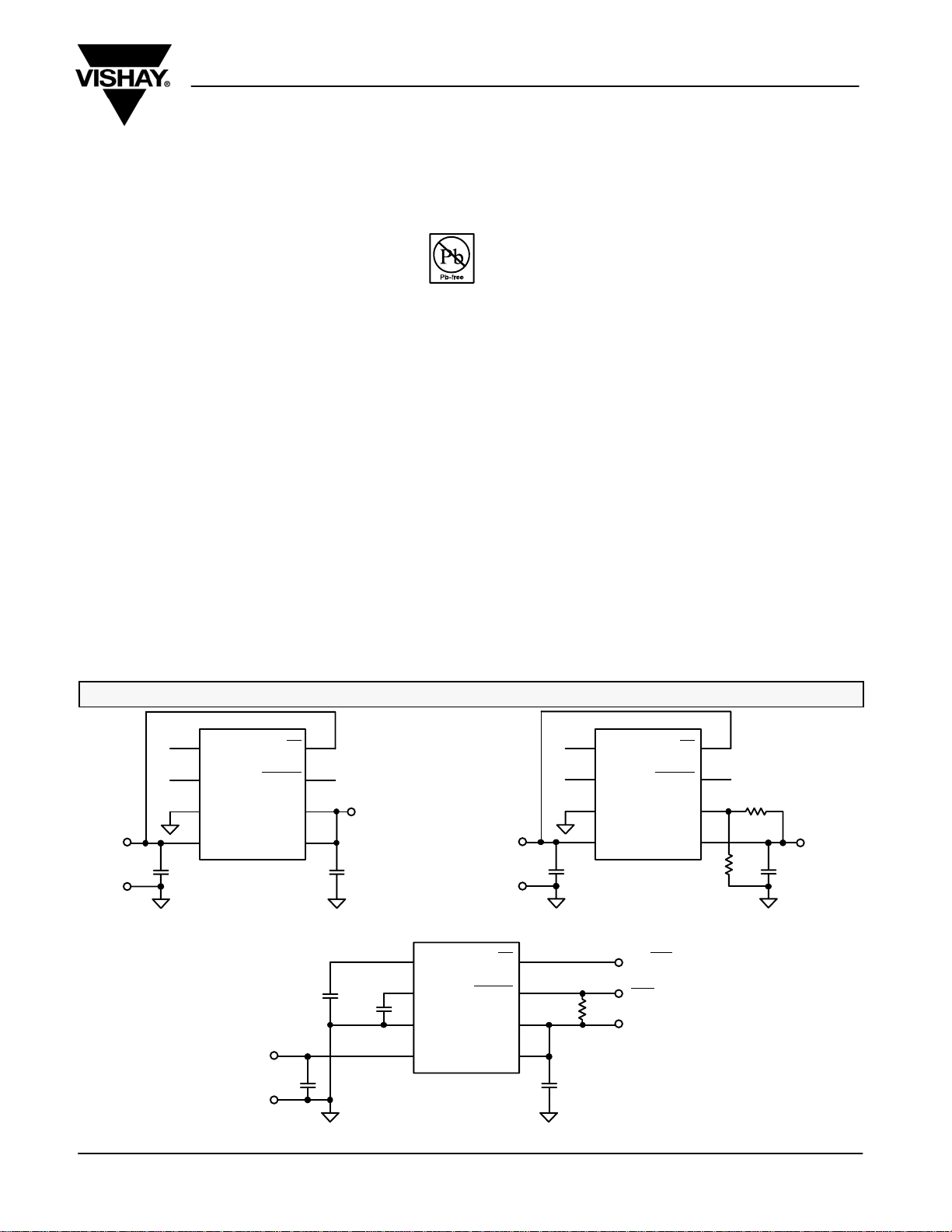
TYPICAL APPLICATIONS CIRCUITS
18
C
NOISE
27
DELAY ERROR
36
GND SENSE/ADJ
45
V
IN
2.2 mF 2.2 mF
GND
V
IN
Si9182
FIGURE 1. Fixed Output FIGURE 2. Adjustable Output
SD
V
OUT
V
OUT
LDO’s output noise for low noise applications.
The Si9182 also includes an out-of-regulation error flag. When
the output voltage is 5% below its nominal output voltage, the
error flag output goes low. If a capacitor is connected to the
device’s delay pin, the error flag output pin will generate a
delayed power-on-reset signal.
The Si9182 is available in both standard and lead (Pb)-free
MSOP-8 packages and is specified to operate over the
industrial temperature range of −40 _C to 85 _C.
18
C
NOISE
27
DELAY ERROR
36
GND SENSE/ADJ
45
V
IN
2.2 mF 2.2 mF
GND
V
IN
Si9182
SD
V
OUT
V
OUT
Document Number: 71150
S-50955—Rev. H, 16-May-05
18
C
NOISE
27
0.1 mF
V
IN
2.2 mF 2.2 mF
GND
0.1 mF
DELAY ERROR
36
GND SENSE/ADJ
45
V
IN
Si9182
SD
V
OUT
FIGURE 3. Low Noise, Full Features Application
1 MW
ON/OFF
POR
V
OUT
www.vishay.com
1
Si9182
y
Output Voltage Accuracy
OUT
%/V
Dropout Voltage
d
IN OUT
(@
)
(@V
t 2 V, VIN w 2 V)
GND
m
Vishay Siliconix
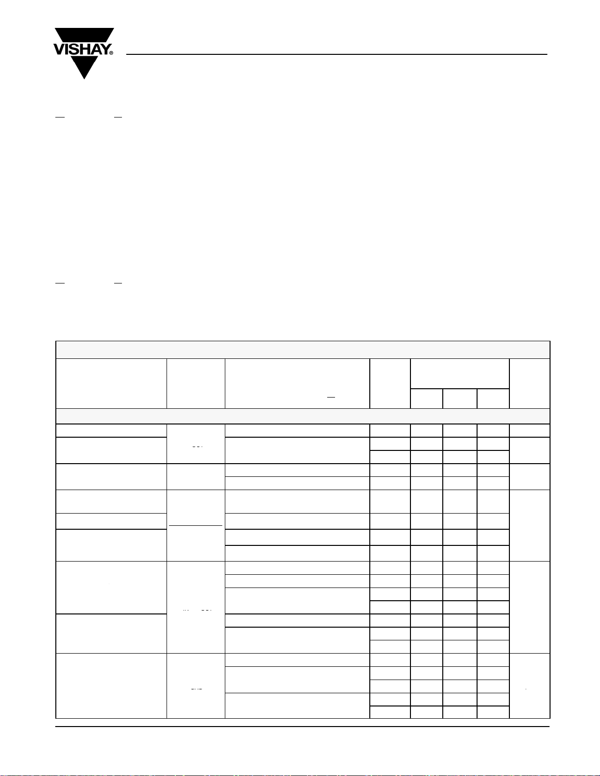
ABSOLUTE MAXIMUM RATINGS
Input Voltage, V
SD Input Voltage, V
Output Current, I
Output Voltage, V
IN
. . . . . . . . . . . . . . . . . . . . . . . . . . . . . . . . .
SD
OUT
OUT
Maximum Junction Temperature, T
Storage Temperature, T
STG
Short Circuit Protected. . . . . . . . . . . . . . . . . . . . . . . . . .
−0.3 V to V
150_C. . . . . . . . . . . . . . . . . . . . . . .
J(max)
−55_C to 150_C. . . . . . . . . . . . . . . . . . . . . . . . . .
−0.3 V to V
+ 0.3 V. . . . . . . . . . . . . . . . . . . . . . . .
O(nom)
6.5 V. . . . . . . . . . . . . . . . . . . . . . . . . . . . . . . . . . . . . . . . . . . .
IN
ESD (Human Body Model) 2 kV. . . . . . . . . . . . . . . . . . . . . . . . . . . . . . . . . . . . .
Stresses beyond those listed under “Absolute Maximum Ratings” may cause permanent damage to the device. These are stress ratings only, and functional operation
of the device at these or any other conditions beyond those indicated in the operational sections of the specifications is not implied. Exposure to absolute maximum rating
Power Dissipation (Package)
8-Pin MSOP 666 mW. . . . . . . . . . . . . . . . . . . . . . . . . . . . . . . . . . . . . . . . . . . . .
Thermal Impedance (Q
8-Pin MSOP
Notes
a. Device mounted with all leads soldered or welded to PC board.
b. Derate 6.6 mW/_C above T
b
conditions for extended periods may affect device reliability.
RECOMMENDED OPERATING RANGE
a
)
JA
= 25_C
A
150_C/W. . . . . . . . . . . . . . . . . . . . . . . . . . . . . . . . . . . . . . . . . . . . .
Input Voltage, V
Output Voltage, V
SD
Input Voltage, V
C
= 2.2 mF, C
IN
C
Range = 1 mF to 10 mF ("10%, x5R or x7R type)
OUT
w C
C
IN
OUT
IN
(Adjustable Version) 1.5 V to 5 V. . . . . . . . . . . . . . . . . .
OUT
. . . . . . . . . . . . . . . . . . . . . . . . . . . . . . . . . . . .
SD
= 2.2 mF (ceramic, X5R or X7R type) , C
OUT
2 V to 6 V. . . . . . . . . . . . . . . . . . . . . . . . . . . . . . . . . . . . . . . .
0 V to V
= 0.1 mF (ceramic)
NOISE
Operating Ambient Temperature, T
Operating Junction Temperature, T
IN
A
J
−40_C to 85_C. . . . . . . . . . . . . . . . . . . .
−40_C to 125_C. . . . . . . . . . . . . . . . . . .
SPECIFICATIONS
T est Conditions
Unless Otherwise Specified
VIN = V
C
Parameter Symbol
= 2.2 mF, C
IN
Output Voltage Range Adjustable Version Full 1.5 5 V
V
DV
OUT
VIN V
VIN − V
OUT
ADJ
100
OUT(nom)
OUT
GND
1 mA v I
From VIN = V
From VIN = 5.5 V to 6 V Full −0.18 0.18
V
= 1.5 V, From VIN = 2.5 V to 3.5 V Full −0.18 0.18
OUT
V
= 5 V, From VIN = 5.5 V to 6 V Full −0.18 0.18
OUT
Output Voltage Accurac
(Fixed Versions)
Feedback Voltage (ADJ Version) V
Line Regulation
(Except 5-V Version)
Line Regulation (5-V Version)
Line Regulation (ADJ Version)
w 2 V)
t 2 V, V
d
d
w 2 V
Dropout Voltage
(@V
OUT
Dropout Voltage
V
OUT
Ground Pin Current I
+ 1 V, I
OUT(nom)
= 2.2 mF, VSD = 1.5 V
OUT
OUT
OUT
v 250 mA
= 1 mA
TempaMinbTypcMax
Room −1.5 1.5
Full −2.5 2.5
Room 1.191 1.215 1.239
Full 1.179 1.251
+ 1 V
OUT(nom)
to V
I
I
OUT
I
OUT
I
OUT
I
OUT
I
OUT
I
OUT
+ 2 V
OUT(nom)
= 10 mA Room 5 20
OUT
= 200 mA Room 85 180
= 250 mA
= 200 mA Room 170 250
= 250 mA
I
= 0 mA Room 150
OUT
= 200 mA
= 250 mA
Full −0.18 0.18
Room 105 275
Full 400
Room 210 300
Full 450
Room 1000
Full 1500
Room 1200
Full 1900
Limits
−40 to 85_C
b
% V
Unit
O(nom)
V
%/V
mV
mA
www.vishay.com
2
Document Number: 71150
S-50955—Rev. H, 16-May-05
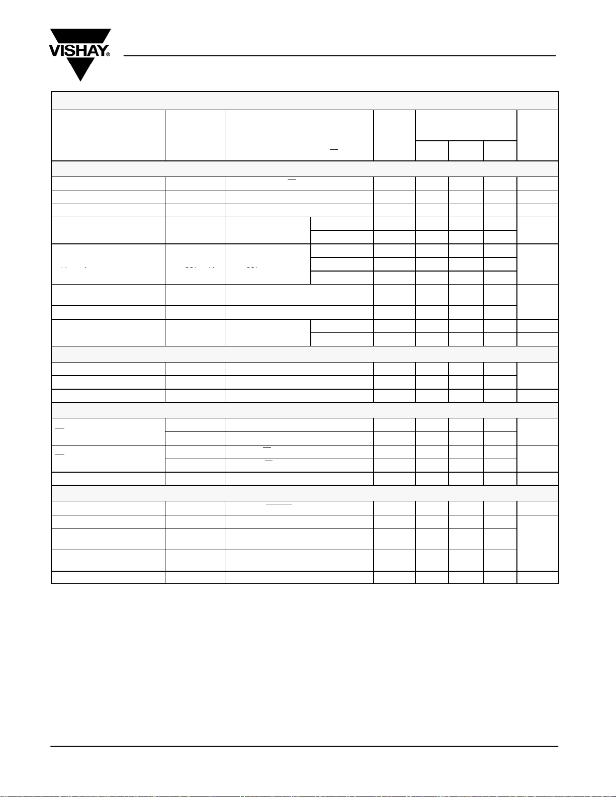
SPECIFICATIONS
BW = 50 Hz to 100 kHz
pp j
OUT IN
OUT
mV
VIN = 4.3 V
Parameter Symbol
T est Conditions
Unless Otherwise Specified
VIN = V
C
= 2.2 mF, C
IN
+ 1 V, I
OUT(nom)
= 2.2 mF, VSD = 1.5 V
OUT
OUT
= 1 mA
Vishay Siliconix
Limits
−40 to 85_C
TempaMinbTypcMax
Si9182
b
Unit
Shutdown Supply Current I
ADJ Pin Current I
Peak Output Current I
O(peak)
Output Noise Voltage e
IN(off)
ADJ
N
V
OUT
BW = 50 Hz to 100 kHz
I
OUT
VSD = 0 V Room 0.1 1 mA
ADJ = 1.2 V Room 5 100 nA
w 0.95 x V
= 150 mA
, tpw = 2 ms Room 500 mA
OUT(nom)
w/o C
NOISE
C
= 0.1 mF Room 100
NOISE
Room 200
f = 1 kHz Room 60
Ripple Rejection DV
OUT
/DV
I
IN
OUT
= 150 mA
f = 10 kHz Room 60
f = 100 kHz Room 40
Dynamic Line Regulation DV
Dynamic Load Regulation DV
V
Turn-On-Time t
OUT
O(line)
O(load)
ON
VIN : V
I
OUT
V
VIN = 4.3 V
OUT
OUT(nom)
t
= 5 ms, I
R/tF
+ 1 V to V
OUT
= 250 mA
OUT(nom)
+ 2 V
Room 10
: 1 mA to 150 mA, tR/tF = 2 ms Room 30
= 3.3 V
w/o C
C
NOISE
Cap Room 5 ms
NOISE
= 0.1 mF Room 2 mS
Thermal Shutdown
Thermal Shutdown Junction Temp t
Thermal Hysteresis t
Short Circuit Current I
J(s/d)
HYST
SC
V
= 0 V Room 800 mA
OUT
Room 165
Room 20
Shutdown Input
SD Input Voltage
SD Input Current
e
Shutdown Hysteresis V
V
IH
V
IL
I
IH
I
IL
HYST
High = Regulator ON (Rising) Full 1.5 V
Low = Regulator OFF (Falling) Full 0.4
VSD = 0 V, Regulator OFF Room 0.01
VSD = 6 V, Regulator ON Room 1.0
Full 100 mV
IN
Error Output
Output High Leakage I
Output Low Voltage
Power_Good Trip Threshold
(Rising)
Hysteresis
g
f, h
f
Delay Pin Current Source I
Notes
a. Room = 25_C, Full = −40 to 85_C.
b. The algebraic convention whereby the most negative value is a minimum and the most positive a maximum.
c. Typical values are for DESIGN AID ONLY, not guaranteed nor subject to production testing. Typical values for dropout voltage at V
V
= 3.3 V, while typical values for dropout voltage at V
OUT
d. Dropout voltage is defined as the input to output differential voltage at which the output voltage drops 2% below the output voltage measured with a 1-V
differential, provided that V
e. The device’s shutdown pin includes a typical 6-MW internal pull-down resistor connected to ground.
f. V
g. The Error Output (Low) function is guaranteed from V
h. The Power_Good trip threshold function is guaranteed from V
is defined as the output voltage of the DUT at 1 mA.
OUT
does not not drop below 2.0 V.
IN
OFF
V
V
V
HYST
DELAY
OL
TH
OUT
ERROR = V
I
= 2 mA Full 0.4
SINK
< 2 V are measured at V
OUT
= 2.0 V to V
OUT
= 5.0 V.
OUT
= 1.5 V to V
OUT(nom)
= 1.8 V.
OUT
= 5.0 V and VIN w 2.0 V.
OUT
Full 0.01 2 mA
Full
Room
0.93 x
V
OUT
0.95 x
V
OUT
2% x
V
OUT
0.97 x
V
OUT
Room 1.2 2.2 3.0 mA
w 2 V are measured at
OUT
mV (rms)
dB
mV
_
_C
V
mA
V
Document Number: 71150
S-50955—Rev. H, 16-May-05
www.vishay.com
3
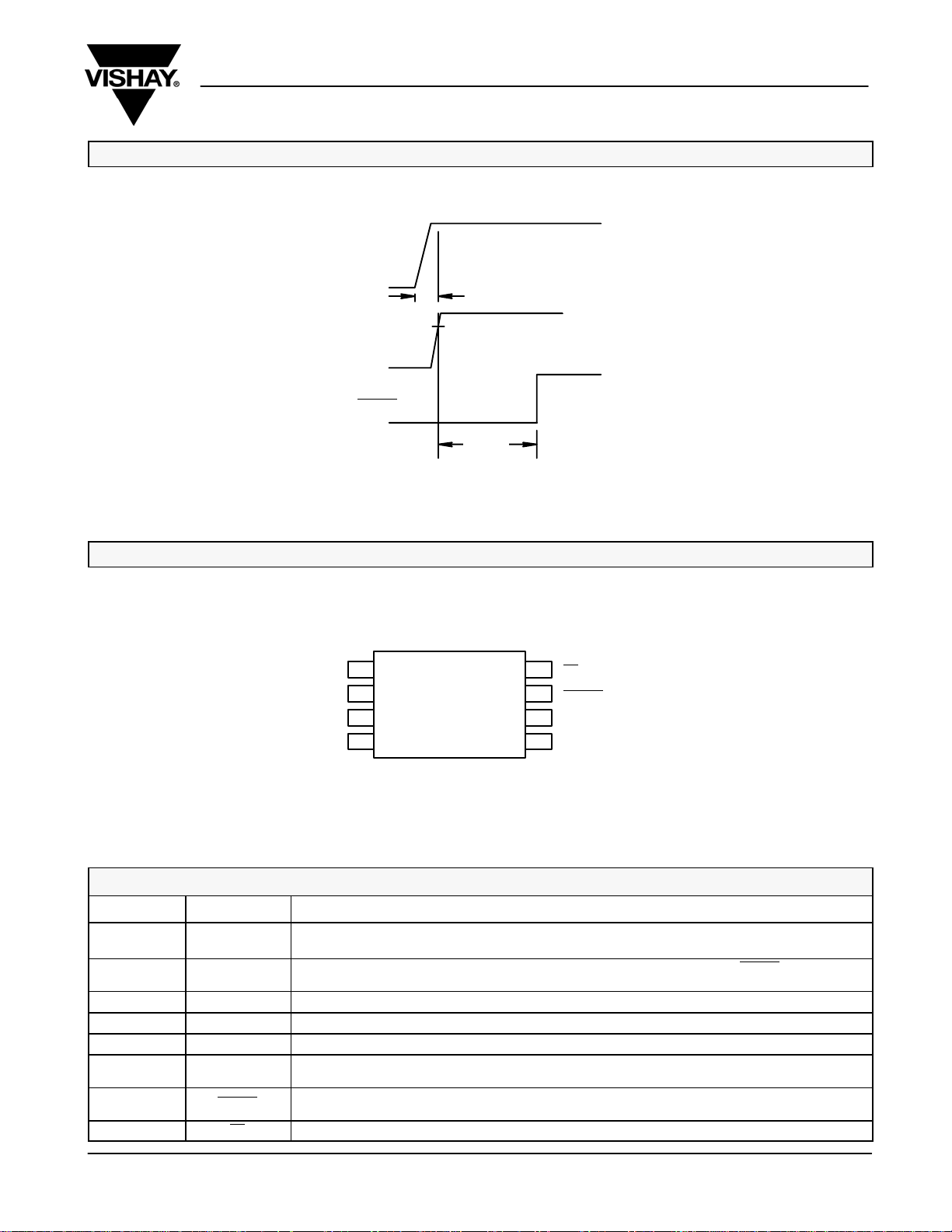
TIMING WAVEFORMS
V
IN
t
ON
0.95 V
NOM
V
OUTVOUT
ERROR
t
DELAY
FIGURE 4. Timing Diagram for Power-Up
V
Si9182
Vishay Siliconix
NOM
PIN CONFIGURATION
MSOP-8
C
NOISE
DELAY ERROR
1
2
GND SENSE or ADJ
3
V
4
IN
Top View
8
SD
7
6
V
5
OUT
PIN DESCRIPTION
Pin Number Name Function
1 C
2 DELAY
3 GND Ground pin. Local ground for C
4 V
5 V
6 SENSE or ADJ
7 ERROR
8 SD By applying less than 0.4 V to this pin, the device will be turned off. Connect this pin to VIN if unused.
NOISE
IN
OUT
Noise bypass pin. For low noise applications, a 0.01-mF or larger ceramic capacitor should be connected from this pin
to ground.
Capacitor connected from this pin to ground will allow a delayed power-on-reset signal at the ERROR (Pin 7) output.
Refer to Figure 4.
and C
NOISE
Input supply pin. Bypass this pin with a 2.2-mF ceramic or tantalum capacitor to ground.
Output voltage. Connect C
For fixed output voltage versions, this pin should be connected to V
this voltage feedback pin sets the output voltage via an external resistor divider.
This open drain output is an error flag output which goes low when V
also provides a power-on-reset signal if a capacitor is connected to the DELAY pin.
between this pin and ground.
OUT
OUT
.
(Pin 5). For adjustable output voltage version,
OUT
drops 5% below its nominal voltage. This pin
OUT
www.vishay.com
4
Document Number: 71150
S-50955—Rev. H, 16-May-05

Vishay Siliconix
_C
MSOP-8
ORDERING INFORMATION
Standard
Part Number
Si9182DH-12-T1 Si9182DH-12-T1—E3 8212 1.215 V
Si9182DH-15-T1 Si9182DH-15-T1—E3 8215 1.5 V
Si9182DH-18-T1 Si9182DH-18-T1—E3 8218 1.8 V
Si9182DH-25-T1 Si9182DH-25-T1—E3 8225 2.5 V
Si9182DH-28-T1 Si9182DH-28-T1—E3 8228 2.8 V
Si9182DH-29-T1 Si9182DH-29-T1—E3 8229 2.9 V
Si9182DH-30-T1 Si9182DH-30-T1—E3 8230 3.0 V
Si9182DH-33-T1 Si9182DH-33-T1—E3 8233 3.3 V
Si9182DH-50-T1 Si9182DH-50-T1—E3 8250 5.0 V
Si9182DH-AD-T1 Si9182DH-AD-T1—E3 82AD Adjustable
* Additional voltage options are available.
TYPICAL CHARACTERISTICS (INTERNALLY REGULATED, 25_C UNLESS NOTED)
Lead (Pb)-Free
Part Number
Marking Voltage
Temperature
Range
−
_
−40 to 85
Eval Kit Temperature Range Board Type
Si9182DB −40 to 85_C Surface Mount
Package
-
Si9182
250
V
= 3.3 V
OUT
200
150
(mV)V
DROP
100
50
0
0 100 200 300 400 500
I
LOAD
(mA)
Dropout Voltage vs. Temperature
180
150
V
= 3.3 V
OUT
120
(mV)V
90
DROP
60
30
0
Dropout Voltage vs. Load Current
−50 −25 0 25 50 75 100 125 150
Junction Temperature (_C)
I
OUT
I
OUT
I
I
OUT
OUT
= 250 mA
= 200 mA
= 10 mA
= 0 mA
3.5
Dropout Characteristic
3.0
R
= 16.5 W
LOAD
2.5
(V)V
2.0
OUT
1.5
1.0
0.5
0.0
0123456
Dropout Voltage vs. V
225
200
175
150
125
100
75
Dropout Voltage (mV)
50
25
0
1.0 1.5 2.0 2.5 3.0 3.5 4.0 4.5 5.0
I
OUT
= 200 mA
VIN (V)
I
V
OUT
OUT
I
OUT
OUT
= 250 mA
= 10 mA
Document Number: 71150
S-50955—Rev. H, 16-May-05
www.vishay.com
5

Vishay Siliconix
TYPICAL CHARACTERISTICS (INTERNALLY REGULATED, 25_C UNLESS NOTED)
Si9182
0.30
0.15
0.00
−0.15
−0.30
Output Voltage (%)
−0.45
−0.60
−0.75
0.0
−0.3
−0.6
(mA)
GND
I
−0.9
Normalized Output Voltage vs. Load Current
0 50 100 150 200 250 300
Load Current (mA)
GND Current vs. Load Current
V
= 5 V
OUT
25_C
−0.0
Normalized V
−0.2
−0.4
(%)V
−0.6
OUT
−0.8
−1.0
−1.2
−40 −20 0 20 40 60 80 100 120 140
I
OUT
Junction Temperature (_C)
vs. Temperature
OUT
= 200 mA
I
OUT
I
= 250 mA
No Load GND Pin Current vs. Input Voltage
300
250
200
mA)
(I
GND
150
100
85_C
25_C
OUT
I
= 0 mA
OUT
= 100 mA
−1.2
−1.5
−20
−40
Gain (dB)
−60
−80
0 50 100 150 200 250
Load Current (mA)
Power Supply Rejection
0
CIN = 10 mF
C
= 2.2 mF
OUT
I
= 150 mA
LOAD
10 100 1000 10000 100000 1000000
Frequency (Hz)
50
0
01234567
GND Pin Current vs. Temperature and Load
1500
1200
900
mA)
(I
GND
600
300
0
−40 −20 0 20 40 60 80 100 120 140
−40_C
Input Voltage (V)
I
= 250 mA
OUT
I
= 200 mA
OUT
I
= 0 mA
OUT
JunctionTemperature (_C)
V
OUT
= 5 V
www.vishay.com
6
Document Number: 71150
S-50955—Rev. H, 16-May-05

TYPICAL WAVEFORMS
Si9182
Vishay Siliconix
V
OUT
10 mV/div
I
LOAD
100 mA/div
5.00 ms/div
V
OUT
10 mV/div
I
LOAD
100 mA/div
Load Transient Response-1
V
= 3.3 V
OUT
C
= 2.2 mF
OUT
I
= 1 to 150 mA
LOAD
t
= 2 msec
rise
Load Transient Response-3
V
OUT
10 mV/div
I
LOAD
100 mA/div
5.00 ms/div
V
OUT
10 mV/div
I
LOAD
100 mA/div
Load Transient Response-2
V
= 3.3 V
OUT
C
= 2.2 mF
OUT
I
= 150 to 1 mA
LOAD
t
= 2 msec
fall
Load Transient Response-4
5.00 ms/div
LineTransient Response-1
V
IN
2 V/div
V
OUT
10 mV/div
5.00 ms/div
Document Number: 71150
S-50955—Rev. H, 16-May-05
V
OUT
C
= 1.0 mF
OUT
I
= 1 to 150 mA
LOAD
t
= 2 msec
rise
V
INSTEP
V
OUT
C
= 2.2 mF
OUT
C
= 10 mF
IN
I
= 250 mA
LOAD
t
= 5 msec
rise
= 3.3 V
= 4.3 to 5.3 V
= 3.3 V
5.00 ms/div
V
OUT
1 V/div
V
OUT
10 mV/div
5.00 ms/div
V
= 3.3 V
OUT
C
= 1.0 mF
OUT
I
= 150 to 1 mA
LOAD
t
= 2 msec
fall
LineTransient Respons-2
V
= 5.3 to 4.3 V
INSTEP
V
= 3.3 V
OUT
C
= 2.2 mF
OUT
C
= 10 mF
IN
I
= 250 mA
LOAD
t
= 5 msec
fall
www.vishay.com
7

TYPICAL WAVEFORMS
Si9182
Vishay Siliconix
VIN 2 V/div
V
2 V/div
OUT
C
2 V/div
delay
ERROR 2 V/div
10.00 ms/div 5.00 ms/div
Turn-On Sequence
V
= 4.2 V
IN
V
= 3.3 V
OUT
C
= 0.1 mF
delay
C
= 0.1 mF
NOISE
I
= 250 mA
LOAD
Output Noise
10.0
Ǹ
mVń Hz
V
CH-3 2 V/div
V
OUT
CH-1 2 V/div
C
delay
CH-4 2 V/div
ERROR
CH-2 2 V/div
Turn-Off Sequence
IN
V
= 4.2 V
IN
V
= 3.3 V
OUT
C
= 0.1 mF
delay
C
= 0.1 mF
NOISE
I
= 250 mA
LOAD
Noise Spectrum
500 mV/div
1 ms/div
V
= 4.2 V
IN
V
= 3.3 V
OUT
I
= 150 mA
OUT
C
= 0.1 mF
NOISE
BW = 10 Hz to 1 MHz
0.01
100 Hz
VIN = 4.1 V
V
= 3.3 V/10 mA
OUT
C
= 0.1 mF
NOISE
1 MHz
www.vishay.com
8
Document Number: 71150
S-50955—Rev. H, 16-May-05

BLOCK DIAGRAMS
6
V
IN
2.2 mF
4
C
IN
SENSE
1C
NOISE
Si9182
Vishay Siliconix
Switches shown for device in normal operating mode (SD = HIGH)
V
SD
ON
IN
SD
ON
GND
C
2.2 mF
GND
OFF
IN
OFF
8
RFB2
6 MW
RFB1
+
−
60 mV
+
+
−
2 mA
To V
IN
5
2
C
OUT
2.2 mF
C
DELAY
0.1 mF
V
OUT
R
EXT
ERROR
1.215 V
3
+
V
REF
−
−
+
7
FIGURE 5. 250-mA CMOS LDO Regulator (Fixed Output)
6
ADJ
4
8
6 MW
60 mV
3
1.215 V
V
REF
1C
NOISE
+
−
+
+
−
R
2
V
ADJ
R
1
To V
IN
2 mA
+
−
5
2
C
OUT
2.2 mF
C
DELAY
0.1 mF
V
OUT
R
EXT
ERROR
−
7
+
Document Number: 71150
S-50955—Rev. H, 16-May-05
FIGURE 6. 250-mA CMOS LDO Regulator (Adjustable Output)
www.vishay.com
9

DETAILED DESCRIPTION
Si9182
Vishay Siliconix
The Si9182 is a low drop out, low quiescent current, and very
linear regulator family with very fast transient response. It is
primarily designed for battery powered applications where
battery run time is at a premium. The low quiescent current
allows extended standby time while low drop out voltage
enables the system to fully utilize battery power before
recharge. The Si9182 is a very fast regulator with bandwidth
exceeding 50 kHz while maintaining low quiescent current at
light load conditions. With this bandwidth, the Si9182 is the
fastest LDO available today. The Si9182 is stable with any
output capacitor type from 1 mF to 10.0 mF. However, X5R or
X7R ceramic capacitors are recommended for best output
noise and transient performance.
V
IN
VIN is the input supply pin. The bypass capacitor for this pin
is not critical as long as the input supply has low enough source
impedance. For practical circuits, a 1.0-mF or larger ceramic
capacitor is recommended. When the source impedance is
not low enough and/or the source is several inches from the
Si9182, then a larger input bypass capacitor is needed. It is
required that the equivalent impedance (source impedance,
wire, and trace impedance in parallel with input bypass
capacitor impedance) must be smaller than the input
impedance of the Si9182 for stable operation. When the
source impedance, wire, and trace impedance are unknown,
it is recommended that an input bypass capacitor be used of
a value that is equal to or greater than the output capacitor.
The formula below calculates the value of R1, given the
desired output voltage and the R2 value,
ǒ
V
R1 +
V
OUT
is nominally 1.215 V.
ADJ
* V
V
ADJ
ADJ
Ǔ
R2
(1)
SHUTDOWN (SD)
controls the turning on and off of the Si9182. V
SD
guaranteed to be on when the SD
greater than 1.5 V. V
is guaranteed to be off when theSD
OUT
pin voltage equals or is
OUT
is
pin voltage equals or is less than 0.4 V. During shutdown
mode, the Si9182 will draw less than 2-mA current from the
source. To automatically turn on V
applied, tie the SD
pin to VIN.
whenever the input is
OUT
ERROR
ERROR is an open drain output that goes low when V
OUT
is
less than 5% of its normal value. As with any open drain output,
an external pull up resistor is needed. When a capacitor is
connected from DELAY to GROUND, the error signal transition
from low to high is delayed (see Delay section). This delayed
error signal can be used as the power-on reset signal for the
application system. (Refer to Figure 4.)
V
OUT
V
is the output voltage of the regulator. Connect a bypass
OUT
capacitor from V
to ground. The output capacitor can be
OUT
any value from 1.0 mF to 10.0 mF. A ceramic capacitor with
X5R or X7R dielectric type is recommended for best output
noise, line transient, and load transient performance.
The ERROR
pin is disconnected if not used.
DELAY
A capacitor from DELAY to GROUND sets the time delay for
ERROR
going from low to high state. The time delay can be
calculated using the following formula:
GND
ǒ
Ǔ
V
Ground is the common ground connection for V
It is also the local ground connection for C
SENSE or ADJ, and SD
.
NOISE
SENSE or ADJ
and V
IN
, DELAY,
OUT
.
T
delay
+
The DELAY pin should be an open circuit if not used.
ADJ
I
delay
C
delay
(2)
SENSE is used to sense the output voltage. Connect SENSE
to V
for the fixed voltage version. For the adjustable output
OUT
C
NOISE
version, use a resistor divider R1 and R2, connect R1 from
V
to ADJ and R2 from ADJ to ground. R2 should be in the
OUT
25-kW to 150-kW range for low power consumption, while
maintaining adequate noise immunity.
Vishay Siliconix maintains worldwide manufact ur ing capability. Products m ay be manufac tured at one of several qualified locations. Re liability data f or Silicon Technology and
Package Reliability represent a composite of all qualified locations. For related documents such as package/tape drawings, part marking, and reliability data, see
http://www.vishay.com/ppg?71 150.
For low noise application, connect a high frequency ceramic
capacitor from C
to ground. A 0.01-mF or a 0.1-mF X5R
NOISE
or X7R is recommended.
www.vishay.com
10
Document Number: 71150
S-50955—Rev. H, 16-May-05

Legal Disclaimer Notice
Vishay
Disclaimer
All product specifications and data are subject to change without notice.
Vishay Intertechnology, Inc., its affiliates, agents, and employees, and all persons acting on its or their behalf
(collectively, “Vishay”), disclaim any and all liability for any errors, inaccuracies or incompleteness contained herein
or in any other disclosure relating to any product.
Vishay disclaims any and all liability arising out of the use or application of any product described herein or of any
information provided herein to the maximum extent permitted by law. The product specifications do not expand or
otherwise modify Vishay’s terms and conditions of purchase, including but not limited to the warranty expressed
therein, which apply to these products.
No license, express or implied, by estoppel or otherwise, to any intellectual property rights is granted by this
document or by any conduct of Vishay.
The products shown herein are not designed for use in medical, life-saving, or life-sustaining applications unless
otherwise expressly indicated. Customers using or selling Vishay products not expressly indicated for use in such
applications do so entirely at their own risk and agree to fully indemnify Vishay for any damages arising or resulting
from such use or sale. Please contact authorized Vishay personnel to obtain written terms and conditions regarding
products designed for such applications.
Product names and markings noted herein may be trademarks of their respective owners.
Document Number: 91000 www.vishay.com
Revision: 18-Jul-08 1

 Loading...