Si9174
High Performance Step-Down DC-DC Converter
With Dynamically Adjustable Output Voltage
FEATURES
D 2-MHz PWM Operation
D Integrated MOSFET Switches
D 2.6-V to 6.0-V Input Voltage Range
D Minimal Number of External Components
D Up to 96% conversion efficiency
D 600-mA Load Capability
D 100% Duty Cycle Allows Low Dropout
D Integrated Compensation Circuit
D Over-Current Protection
D Shutdown Current < 2 mA
D Thermal Shutdown
D Integrated UVLO
D 10-Pin MSOP and Space Saving MLP33 Packaging
D DAC Input for Dynamic Output Voltage Adjustment
DESCRIPTION
New Product
Vishay Siliconix
D Synchronizable to13-MHz Clock
D User Selectable PWM, PSM, or AUTO Mode
D PSM Frequency w20 kHz for Inaudible
Harmonics
APPLICATIONS
D W-CDMA Cell Phone
D PDAs/Palmtop PCs
D LCD Modules
D Portable Image Scanners
D GPS Receivers
D Smart Phones
D MP3 Players
D 3G Cell Phone
D Digital Cameras
The Si9174 is a high efficiency 600-mA step down converter
with internal low on resistance power MOSFET switch and
synchronous rectifier transistors. It is designed to convert one
cell LiIon battery or three cell alkaline battery voltages to a
dynamically adjustable dc output. The voltage on the DAC pin
controls the output voltage. The output voltage is adjustable
between 0.4 V and the input voltage VIN less a small dropout
voltage and settles in <30 ms.
In order to insure efficient conversion throughout the entire
load range, PWM (pulse width modulation), PSM (pulse
skipping mode) or Auto mode can be selected. In PWM mode,
2-MHz switching permits use of small external inductor and
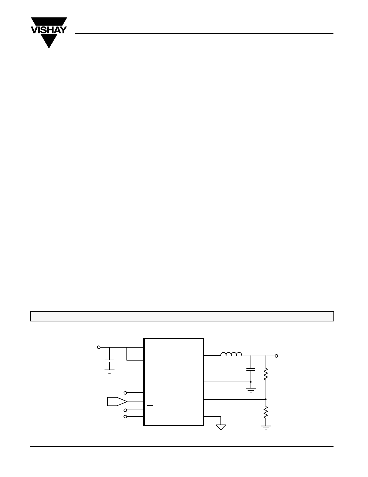
TYPICAL APPLICATIONS CIRCUIT
BATTERY
C
IN
10 mF
PWM/PSM/AUTO
13 MHz
DAC
ENABLE
V
IN
V
DD
SYNC
DAC
SD
MODE
Si9174
capacitor sizes allowing one of the smallest solutions. To
minimize system noise, the switching frequency can be
synchronized to an external 13-MHz clock.
PSM mode provides increased efficiency at light loads. In PSM
mode the oscillator frequency is kept above 20 kHz to avoid
audio band interference. When operating in Auto mode, the
converter automatically selects operating in either PWM or
PSM mode according to load current demand.
The Si9174 is available in 10-pin MSOP and even smaller
MLP33 packages and is specified to operate over the
industrial temperature range of –40_C to 85_C.
LX
PGND
FB
AGND
2.2 mH
C
4.7 mF
OUT
V
OUT
R
1
R
2
Document Number: 71668
S-21824—Rev. A, 07-Oct-02
www.vishay.com
1

Si9174
Vishay Siliconix
New Product
ABSOLUTE MAXIMUM RATINGS
Voltages Referenced to AGND = 0 V
V
IN, VDD
Lx, SD, MODE, FB, DAC, SYNC -0.3 to 6.2 V. . . . . . . . . . . . . . . . . . . . . . . . . . . . . . .
GND -0.3 to +0.3 V
. . . . . . . . . . . . . . . . . . . . . . . . . . . . . . . . . . . . . . . . . . . . . . . . . . . . . . . . . . . .
ESD Rating 2 kV. . . . . . . . . . . . . . . . . . . . . . . . . . . . . . . . . . . . . . . . . . . . . . . . . . . . . . . . . . . . . . .
Storage Temperature -65 to 125_C. . . . . . . . . . . . . . . . . . . . . . . . . . . . . . . . . . . . . . . . . .
Operating Junction Temperature 150_C. . . . . . . . . . . . . . . . . . . . . . . . . . . . . . . . . . . . . . .
Power Dissipation (Package)
10-pin MSOP
10-pin MLP33 915 mW. . . . . . . . . . . . . . . . . . . . . . . . . . . . . . . . . . . . . . . . . . . . . . . . . . . . . . . .
Stresses beyond those listed under “Absolute Maximum Ratings” may cause permanent damage to the device. These are stress ratings only, and functional operation
of the device at these or any other conditions beyond those indicated in the operational sections of the specifications is not implied. Exposure to absolute maximum rating
conditions for extended periods may affect device reliability.
b
(or to VDD )0.3 V whichever is less)
a
6.2 V. . . . . . . . . . . . . . . . . . . . . . . . . . . . . . . . . . . . . . . . . . . . . . . . . . . . . . . . . . . . . . . . .
481 mW. . . . . . . . . . . . . . . . . . . . . . . . . . . . . . . . . . . . . . . . . . . . . . . . . . . . . . . .
Thermal Impedance (QJA)
10-Pin MSOP 135_C/W
10-Pin MLP33 71_C/W. . . . . . . . . . . . . . . . . . . . . . . . . . . . . . . . . . . . . . . . . . . . . . . . . . . . . . . .
Peak Inductor Current 1.8 A. . . . . . . . . . . . . . . . . . . . . . . . . . . . . . . . . . . . . . . . . . . . . . . . . .
Notes
a. Device mounted with all leads soldered or welded to PC board.
b. Derate 7.4 mW/_C above 85_C.
c. Derate 14 mW/_C above 85_ C.
. . . . . . . . . . . . . . . . . . . . . . . . . . . . . . . . . . . . . . . . . . . . . . . . . . . . . . .
RECOMMENDED OPERATING RANGE
VIN Range 2.6 V to 5.5 V. . . . . . . . . . . . . . . . . . . . . . . . . . . . . . . . . . . . . . . . . . .
C
IN
4.7 mF Ceramic. . . . . . . . . . . . . . . . . . . . . . . . . . . . . . . . . . . . . . . . . . . . .
C
OUT
10 mF Ceramic. . . . . . . . . . . . . . . . . . . . . . . . . . . . . . . . . . . . . . . . . . . . . . . .
Inductor 2.2 mH. . . . . . . . . . . . . . . . . . . . . . . . . . . . . . . . . . . . . . . . . . . . . . . . . . .
Operating Load Current PWM Mode 0 to 600 mA. . . . . . . . . . . . . . . . . . . . . .
Operating Load Current PSM Mode 0 to 150 mA. . . . . . . . . . . . . . . . . . . . . . .
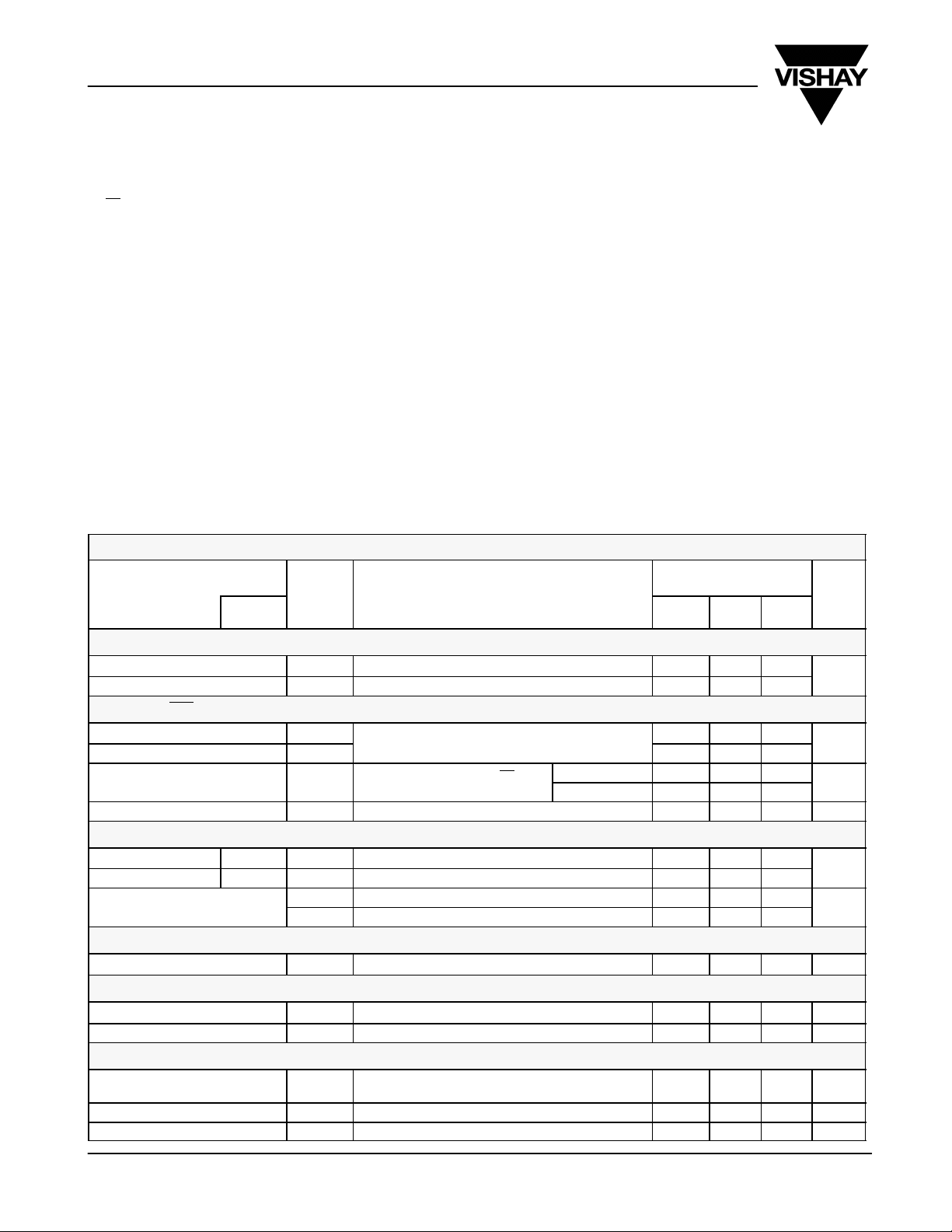
SPECIFICATIONS
Parameter
ModefSymbol
T est Conditions Unless Specified
_ _
-40_C to 85_C, VIN = V
C
= 4.7 mF, L = 2.2 mH, 2.6 V v VIN v 5.5 V
OUT
R
1
V
= 1.215 V, CIN = 10 mF,
DD,
DAC
= 11.3 kW, R2 = 20 kW
Limits
MinaTypbMaxaUnit
Under Voltage Lockout (UVLO)
Under V oltage Lockout (turn-on) VIN rising 2.3 2.5
Hysteresis 0.1
Shutdown (SD)
Logic HIGH V
Logic LOW V
Delay to Output
Pull Down I
c
SDH
SDL
t
en
SD
Settle Within $2% accuracy SD rising
Settle Within $2% accuracy SD rising
t
< 1 ms
r
Input at V
IN
RL = 3.3 W 100
RL = 51 W 100
1.6
0.4
Mode Selection Tri-Level Logic (MODE)
MODE Pin HIGH PWM VIN -0.4 V
MODE Pin LOW Auto 0.4
Mode Pin Input Current
MODE = GND -5
MODE = V
IN
IN
5
Oscillator
Frequency f
OSC
1.6 2 2.4 MHz
External Clock Synchronization (SYNC)
Frequency SYNC Input = 500 mV
Ac Coupled Sinewave Frequency = 13 MHz 0.2 0.8 V
p-p
13 MHz
Error Amplifier (FB, DAC Pin)
FB Voltage Accuracy
DAC Input Voltage Range V
Input Bias Current FB, DAC I
FBDAC
V
DAC
-20
> 2.6, V
IN
V
> 0.5 V 0.28 2.45 V
IN -
DAC
VFB = 1.25 V -1 0.01 1 mA
V
DAC
+20
V
V
ms
mA
V
mA
p-p
mV
www.vishay.com
2
Document Number: 71668
S-21824—Rev. A, 07-Oct-02

Si9174
New Product
Vishay Siliconix
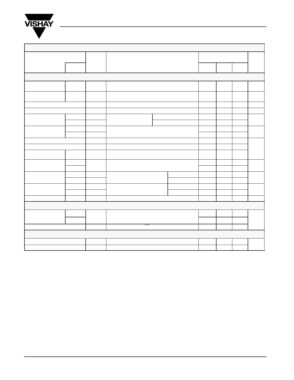
SPECIFICATIONS
T est Conditions Unless Specified
Parameter Limits
f
SymbolMode
Converter Operation
Maximum Output
Current
Maximum Output
Current
Dropout Voltage
e
Closed Loop Bandwidth BW 300 kHz
Load Regulation
c
Line Regulation
PWM/PSM Switch Threshold Current I
Maximum Inductor Peak Current Limit I
Maximum NMOS
Transistor Current Sink
On Resistance
Output Ripple Voltage
Efficiency
Frequency PSM I
PWM I
PSM I
LOAD
LOAD
V
DD
PWM
PSM
PWM "0.1
PSM
AUpk
Lpk
PWM Negative Transition on V
P-Channel 250
N-Channel
r
DS(on)
PWM
PSM
PWM I
PSM
Supply Current
Input Supply Current
PWM
PSM
Shutdown Supply Current I
I
SUPPLY
(V
DD
V
IN
SD
&
)
Thermal Shutdown
Thermal Shutdown Temperature
Thermal Hysteresis
Notes
a. The algebraic convention whereby the most negative value is a minimum and the most positive a maximum, is used in this data sheet.
b. Typical values are for DESIGN AID ONLY, not guaranteed or subject to production testing.
c. Guaranteed by design.
d. Settling times, t
e. Bypass is a device mode of operation, in which, the device is in 100% duty cycle. Bypass operation is possible in either PWM or PSM.
f. Operating modes are controlled with the MODE pin where Auto mode = MODE = LOW, PWM Mode = MODE = HIGH, and PSM mode = MODE = OPEN.
c
, apply after ten.
s
c
T
J(S/D)
T est Conditions Unless Specified
-40_C to 85_C, VIN = V
-40_C to 85_C, VIN = V
C
C
= 4.7 mF, L = 2.2 mH, 2.6 V v VIN v 5.5 V
= 4.7 mF, L = 2.2 mH, 2.6 V v VIN v 5.5 V
OUT
OUT
R
R
1
1
VIN = 2.6 V, I
VIN = 3.6 V
VIN = 3.6 V
V
= 1.9 V @ 25_C
OUT
V
= 3.0 V, VIN = 3.5 V to 5.5 V
OUT
0.05 W C
VIN = 3.6 V, V
I
= 0 mA, VIN = 3.6 V (not switching, FB = GND)
OUT
V
= 1.215 V, CIN = 10 mF,
V
= 1.215 V, CIN = 10 mF,
DD,
DAC
DD,
DAC
= 11.3 kW, R2 = 20 kW
= 11.3 kW, R2 = 20 kW
VIN = 3.6 V 600 mA
VIN = 3.6 V 150 mA
= 600 mA 190 300 mV
OUT
I
= 30 mA to 600 mA 0.5
OUT
I
= 30 mA to 75 mA 0.25
OUT
VIN = 3.6 V
OUT(ESR)
= 3.3 V
OUT
w 30 mA 20 kHz
OUT
SD = Low 2
DAC
I
= 600 mA 60
OUT
I
= 30 mA 80
OUT
= 600 mA 90
OUT
I
= 30 mA 80
OUT
Min
a
b
Typ
"0.1
200
1500
1500
250
500 800
400
165
20
a
UnitMax
mV
%
%/V
mA
mA
mW
%
mA
_
_C
p-p
Document Number: 71668
S-21824—Rev. A, 07-Oct-02
www.vishay.com
3

Si9174
Vishay Siliconix
New Product
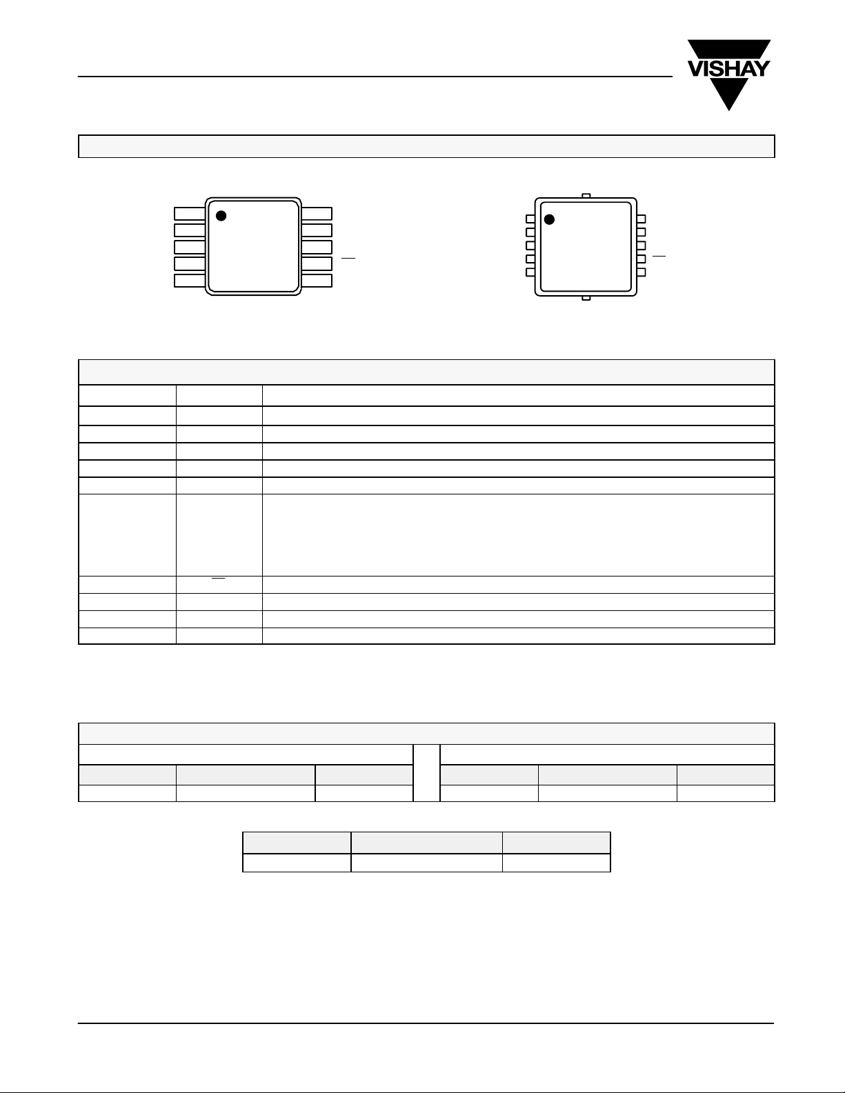
PIN CONFIGURATION
MSOP-10
1
L
X
AGND V
DAC MODE
2
3
FB SYNC
47
V
DD
56
Top View
10
PGND
9
IN
8
SD
AGND
V
PIN DESCRIPTION
Pin Number Name Function
1 L
2 AGND Low power analog ground
3 FB Output voltage feedback
4 V
5 DAC Voltage from external DAC to adjust output voltage.
6 MODE
7 SD Logic low disables IC and reduces quiescent current to below 2 mA
8 SYNC Converter switching frequency can be synchronized to 1/6 of the clock frequency at this pin.
9 V
10 PGND Low impedance power ground
X
DD
IN
Inductor connection
Input supply voltage for the analog circuit.
Used to select switching mode of the buck converter
PWM/PSM Pin Logic:
MODE Pin Operating Mode
V
IN
Open PSM
GND AUTO
Input supply voltage
PWM
MLP33
L
X
2
3
FB
4
DD
5DAC 6 MODE
T op View
10
PGND
9
V
IN
8
SYNC
7
SD
ORDERING INFORMATION
MSOP-10 MLP33
Part Number Marking Temperature Part Number Marking Temperature
Si9174DH-T1 9174 -40 to 85_C Si9174DM-T1 9174 -40 to 85_C
Additional voltage options are available.
Eval Kit T emperature Range Board
Si9174DB -40 to 85_ C Surface Mount
www.vishay.com
4
Document Number: 71668
S-21824—Rev. A, 07-Oct-02
 Loading...