

Si9174
High Performance Step-Down DC-DC Converter
With Dynamically Adjustable Output Voltage
FEATURES
D 2-MHz PWM Operation
D Integrated MOSFET Switches
D 2.6-V to 6.0-V Input Voltage Range
D Minimal Number of External Components
D Up to 96% conversion efficiency
D 600-mA Load Capability
D 100% Duty Cycle Allows Low Dropout
D Integrated Compensation Circuit
D Over-Current Protection
D Shutdown Current < 2 mA
D Thermal Shutdown
D Integrated UVLO
D 10-Pin MSOP and Space Saving MLP33 Packaging
D DAC Input for Dynamic Output Voltage Adjustment
DESCRIPTION
New Product
Vishay Siliconix
D Synchronizable to13-MHz Clock
D User Selectable PWM, PSM, or AUTO Mode
D PSM Frequency w20 kHz for Inaudible
Harmonics
APPLICATIONS
D W-CDMA Cell Phone
D PDAs/Palmtop PCs
D LCD Modules
D Portable Image Scanners
D GPS Receivers
D Smart Phones
D MP3 Players
D 3G Cell Phone
D Digital Cameras
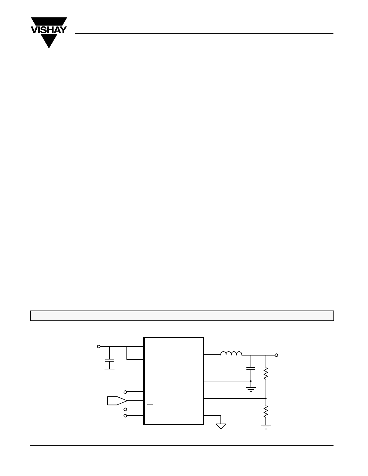
The Si9174 is a high efficiency 600-mA step down converter
with internal low on resistance power MOSFET switch and
synchronous rectifier transistors. It is designed to convert one
cell LiIon battery or three cell alkaline battery voltages to a
dynamically adjustable dc output. The voltage on the DAC pin
controls the output voltage. The output voltage is adjustable
between 0.4 V and the input voltage VIN less a small dropout
voltage and settles in <30 ms.
In order to insure efficient conversion throughout the entire
load range, PWM (pulse width modulation), PSM (pulse
skipping mode) or Auto mode can be selected. In PWM mode,
2-MHz switching permits use of small external inductor and
TYPICAL APPLICATIONS CIRCUIT
BATTERY
C
IN
10 mF
PWM/PSM/AUTO
13 MHz
DAC
ENABLE
V
IN
V
DD
SYNC
DAC
SD
MODE
Si9174
capacitor sizes allowing one of the smallest solutions. To
minimize system noise, the switching frequency can be
synchronized to an external 13-MHz clock.
PSM mode provides increased efficiency at light loads. In PSM
mode the oscillator frequency is kept above 20 kHz to avoid
audio band interference. When operating in Auto mode, the
converter automatically selects operating in either PWM or
PSM mode according to load current demand.
The Si9174 is available in 10-pin MSOP and even smaller
MLP33 packages and is specified to operate over the
industrial temperature range of –40_C to 85_C.
LX
PGND
FB
AGND
2.2 mH
C
4.7 mF
OUT
V
OUT
R
1
R
2
Document Number: 71668
S-21824—Rev. A, 07-Oct-02
www.vishay.com
1
Si9174
Vishay Siliconix
New Product
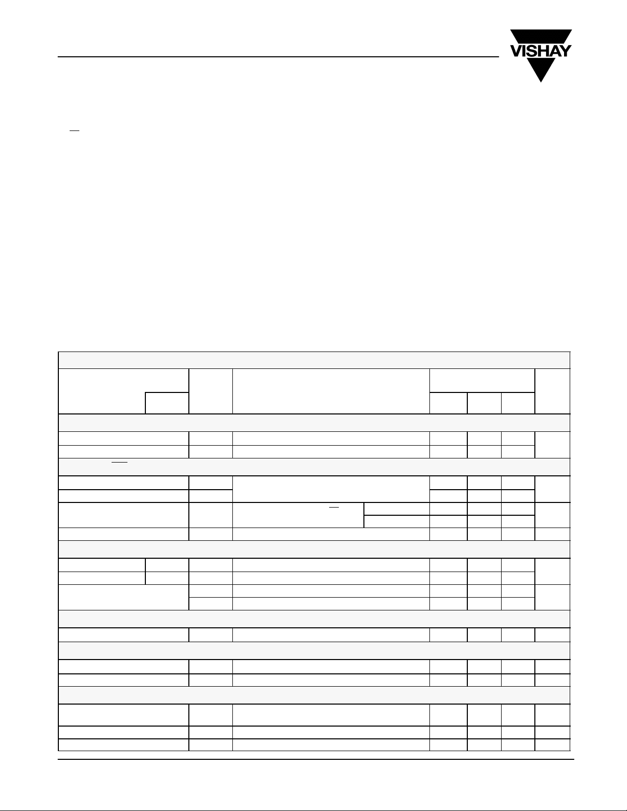
ABSOLUTE MAXIMUM RATINGS
Voltages Referenced to AGND = 0 V
V
IN, VDD
Lx, SD, MODE, FB, DAC, SYNC -0.3 to 6.2 V. . . . . . . . . . . . . . . . . . . . . . . . . . . . . . .
GND -0.3 to +0.3 V
. . . . . . . . . . . . . . . . . . . . . . . . . . . . . . . . . . . . . . . . . . . . . . . . . . . . . . . . . . . .
ESD Rating 2 kV. . . . . . . . . . . . . . . . . . . . . . . . . . . . . . . . . . . . . . . . . . . . . . . . . . . . . . . . . . . . . . .
Storage Temperature -65 to 125_C. . . . . . . . . . . . . . . . . . . . . . . . . . . . . . . . . . . . . . . . . .
Operating Junction Temperature 150_C. . . . . . . . . . . . . . . . . . . . . . . . . . . . . . . . . . . . . . .
Power Dissipation (Package)
10-pin MSOP
10-pin MLP33 915 mW. . . . . . . . . . . . . . . . . . . . . . . . . . . . . . . . . . . . . . . . . . . . . . . . . . . . . . . .
Stresses beyond those listed under “Absolute Maximum Ratings” may cause permanent damage to the device. These are stress ratings only, and functional operation
of the device at these or any other conditions beyond those indicated in the operational sections of the specifications is not implied. Exposure to absolute maximum rating
conditions for extended periods may affect device reliability.
b
(or to VDD )0.3 V whichever is less)
a
6.2 V. . . . . . . . . . . . . . . . . . . . . . . . . . . . . . . . . . . . . . . . . . . . . . . . . . . . . . . . . . . . . . . . .
481 mW. . . . . . . . . . . . . . . . . . . . . . . . . . . . . . . . . . . . . . . . . . . . . . . . . . . . . . . .
Thermal Impedance (QJA)
10-Pin MSOP 135_C/W
10-Pin MLP33 71_C/W. . . . . . . . . . . . . . . . . . . . . . . . . . . . . . . . . . . . . . . . . . . . . . . . . . . . . . . .
Peak Inductor Current 1.8 A. . . . . . . . . . . . . . . . . . . . . . . . . . . . . . . . . . . . . . . . . . . . . . . . . .
Notes
a. Device mounted with all leads soldered or welded to PC board.
b. Derate 7.4 mW/_C above 85_C.
c. Derate 14 mW/_C above 85_ C.
. . . . . . . . . . . . . . . . . . . . . . . . . . . . . . . . . . . . . . . . . . . . . . . . . . . . . . .
RECOMMENDED OPERATING RANGE
VIN Range 2.6 V to 5.5 V. . . . . . . . . . . . . . . . . . . . . . . . . . . . . . . . . . . . . . . . . . .
C
IN
4.7 mF Ceramic. . . . . . . . . . . . . . . . . . . . . . . . . . . . . . . . . . . . . . . . . . . . .
C
OUT
10 mF Ceramic. . . . . . . . . . . . . . . . . . . . . . . . . . . . . . . . . . . . . . . . . . . . . . . .
Inductor 2.2 mH. . . . . . . . . . . . . . . . . . . . . . . . . . . . . . . . . . . . . . . . . . . . . . . . . . .
Operating Load Current PWM Mode 0 to 600 mA. . . . . . . . . . . . . . . . . . . . . .
Operating Load Current PSM Mode 0 to 150 mA. . . . . . . . . . . . . . . . . . . . . . .
SPECIFICATIONS
Parameter
ModefSymbol
T est Conditions Unless Specified
_ _
-40_C to 85_C, VIN = V
C
= 4.7 mF, L = 2.2 mH, 2.6 V v VIN v 5.5 V
OUT
R
1
V
= 1.215 V, CIN = 10 mF,
DD,
DAC
= 11.3 kW, R2 = 20 kW
Limits
MinaTypbMaxaUnit
Under Voltage Lockout (UVLO)
Under V oltage Lockout (turn-on) VIN rising 2.3 2.5
Hysteresis 0.1
Shutdown (SD)
Logic HIGH V
Logic LOW V
Delay to Output
Pull Down I
c
SDH
SDL
t
en
SD
Settle Within $2% accuracy SD rising
Settle Within $2% accuracy SD rising
t
< 1 ms
r
Input at V
IN
RL = 3.3 W 100
RL = 51 W 100
1.6
0.4
Mode Selection Tri-Level Logic (MODE)
MODE Pin HIGH PWM VIN -0.4 V
MODE Pin LOW Auto 0.4
Mode Pin Input Current
MODE = GND -5
MODE = V
IN
IN
5
Oscillator
Frequency f
OSC
1.6 2 2.4 MHz
External Clock Synchronization (SYNC)
Frequency SYNC Input = 500 mV
Ac Coupled Sinewave Frequency = 13 MHz 0.2 0.8 V
p-p
13 MHz
Error Amplifier (FB, DAC Pin)
FB Voltage Accuracy
DAC Input Voltage Range V
Input Bias Current FB, DAC I
FBDAC
V
DAC
-20
> 2.6, V
IN
V
> 0.5 V 0.28 2.45 V
IN -
DAC
VFB = 1.25 V -1 0.01 1 mA
V
DAC
+20
V
V
ms
mA
V
mA
p-p
mV
www.vishay.com
2
Document Number: 71668
S-21824—Rev. A, 07-Oct-02
Si9174
New Product
Vishay Siliconix
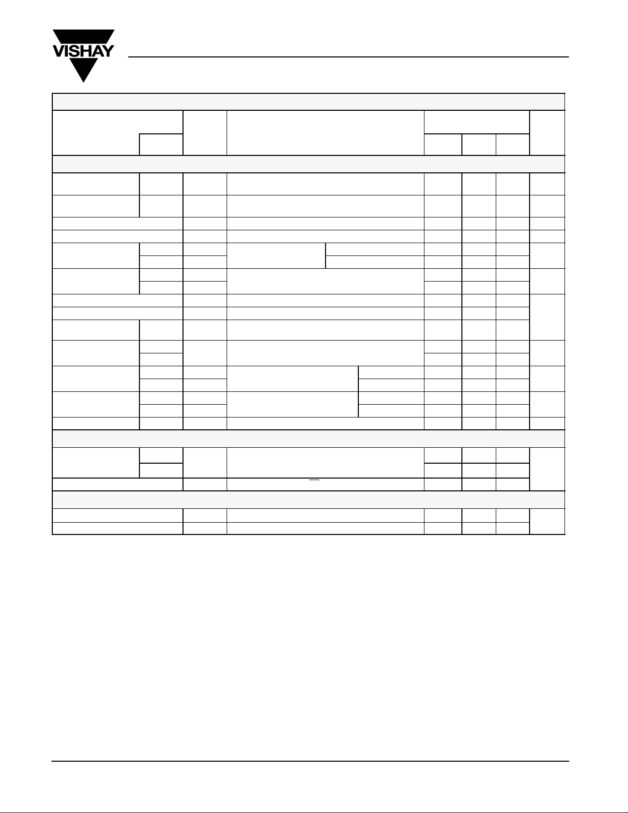
SPECIFICATIONS
T est Conditions Unless Specified
Parameter Limits
f
SymbolMode
Converter Operation
Maximum Output
Current
Maximum Output
Current
Dropout Voltage
e
Closed Loop Bandwidth BW 300 kHz
Load Regulation
c
Line Regulation
PWM/PSM Switch Threshold Current I
Maximum Inductor Peak Current Limit I
Maximum NMOS
Transistor Current Sink
On Resistance
Output Ripple Voltage
Efficiency
Frequency PSM I
PWM I
PSM I
LOAD
LOAD
V
DD
PWM
PSM
PWM "0.1
PSM
AUpk
Lpk
PWM Negative Transition on V
P-Channel 250
N-Channel
r
DS(on)
PWM
PSM
PWM I
PSM
Supply Current
Input Supply Current
PWM
PSM
Shutdown Supply Current I
I
SUPPLY
(V
DD
V
IN
SD
&
)
Thermal Shutdown
Thermal Shutdown Temperature
Thermal Hysteresis
Notes
a. The algebraic convention whereby the most negative value is a minimum and the most positive a maximum, is used in this data sheet.
b. Typical values are for DESIGN AID ONLY, not guaranteed or subject to production testing.
c. Guaranteed by design.
d. Settling times, t
e. Bypass is a device mode of operation, in which, the device is in 100% duty cycle. Bypass operation is possible in either PWM or PSM.
f. Operating modes are controlled with the MODE pin where Auto mode = MODE = LOW, PWM Mode = MODE = HIGH, and PSM mode = MODE = OPEN.
c
, apply after ten.
s
c
T
J(S/D)
T est Conditions Unless Specified
-40_C to 85_C, VIN = V
-40_C to 85_C, VIN = V
C
C
= 4.7 mF, L = 2.2 mH, 2.6 V v VIN v 5.5 V
= 4.7 mF, L = 2.2 mH, 2.6 V v VIN v 5.5 V
OUT
OUT
R
R
1
1
VIN = 2.6 V, I
VIN = 3.6 V
VIN = 3.6 V
V
= 1.9 V @ 25_C
OUT
V
= 3.0 V, VIN = 3.5 V to 5.5 V
OUT
0.05 W C
VIN = 3.6 V, V
I
= 0 mA, VIN = 3.6 V (not switching, FB = GND)
OUT
V
= 1.215 V, CIN = 10 mF,
V
= 1.215 V, CIN = 10 mF,
DD,
DAC
DD,
DAC
= 11.3 kW, R2 = 20 kW
= 11.3 kW, R2 = 20 kW
VIN = 3.6 V 600 mA
VIN = 3.6 V 150 mA
= 600 mA 190 300 mV
OUT
I
= 30 mA to 600 mA 0.5
OUT
I
= 30 mA to 75 mA 0.25
OUT
VIN = 3.6 V
OUT(ESR)
= 3.3 V
OUT
w 30 mA 20 kHz
OUT
SD = Low 2
DAC
I
= 600 mA 60
OUT
I
= 30 mA 80
OUT
= 600 mA 90
OUT
I
= 30 mA 80
OUT
Min
a
b
Typ
"0.1
200
1500
1500
250
500 800
400
165
20
a
UnitMax
mV
%
%/V
mA
mA
mW
%
mA
_
_C
p-p
Document Number: 71668
S-21824—Rev. A, 07-Oct-02
www.vishay.com
3
Si9174
Vishay Siliconix
New Product
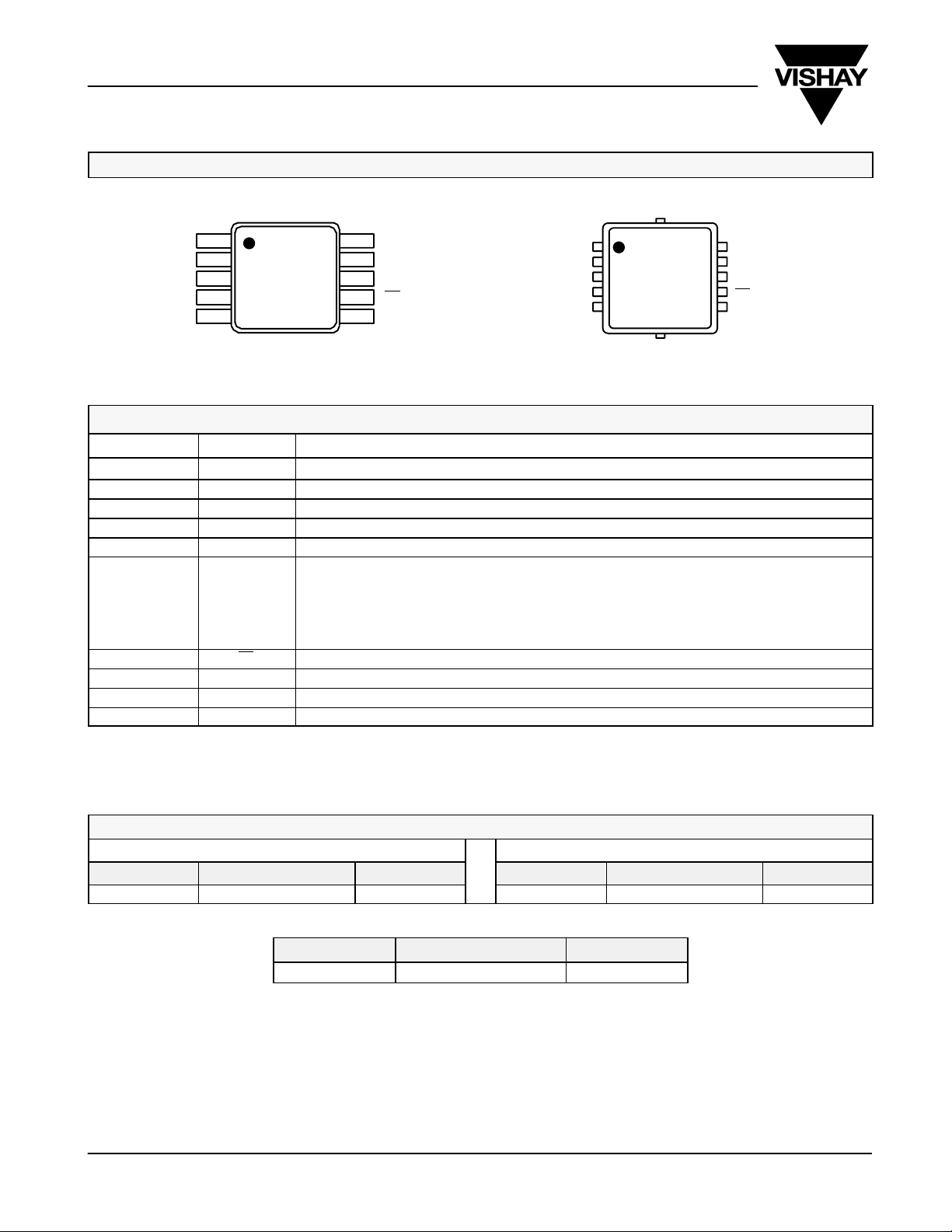
PIN CONFIGURATION
MSOP-10
1
L
X
AGND V
DAC MODE
2
3
FB SYNC
47
V
DD
56
Top View
10
PGND
9
IN
8
SD
AGND
V
PIN DESCRIPTION
Pin Number Name Function
1 L
2 AGND Low power analog ground
3 FB Output voltage feedback
4 V
5 DAC Voltage from external DAC to adjust output voltage.
6 MODE
7 SD Logic low disables IC and reduces quiescent current to below 2 mA
8 SYNC Converter switching frequency can be synchronized to 1/6 of the clock frequency at this pin.
9 V
10 PGND Low impedance power ground
X
DD
IN
Inductor connection
Input supply voltage for the analog circuit.
Used to select switching mode of the buck converter
PWM/PSM Pin Logic:
MODE Pin Operating Mode
V
IN
Open PSM
GND AUTO
Input supply voltage
PWM
MLP33
L
X
2
3
FB
4
DD
5DAC 6 MODE
T op View
10
PGND
9
V
IN
8
SYNC
7
SD
ORDERING INFORMATION
MSOP-10 MLP33
Part Number Marking Temperature Part Number Marking Temperature
Si9174DH-T1 9174 -40 to 85_C Si9174DM-T1 9174 -40 to 85_C
Additional voltage options are available.
Eval Kit T emperature Range Board
Si9174DB -40 to 85_ C Surface Mount
www.vishay.com
4
Document Number: 71668
S-21824—Rev. A, 07-Oct-02

Si9174
FUNCTIONAL BLOCK DIAGRAM
V
DD V
FB
DAC
Voltage
Reference
UVLO
AGND MODE SD
+
B6
SYNC
Error
Amplifier
To IC Bias
New Product
Si9174
Clamp
2 MHz
2 MHz
Oscillator
Oscillator
+
PWM
Comparator
IN
PWM and
Pulse
Skipping
Logic
PMOS
Current Sense
NMOS
Current Sense
Vishay Siliconix
L
X
PGND
DETAIL DESCRIPTION
General
The Si9174 is a high efficiency synchronous dc-dc converter
that is ideally suited for lithium ion battery or three cell alkaline
applications, as well as step-down of 3.3-V or 5.0-V supplies.
It is design to provide power to the power amplifier in WCDMA
cell phones, but can utilized in any applications requiring a
dynamically adjustable 600-mA power supply. The major
blocks of the Si9174 are shown in the Functional Block
Diagram. The 0.25-W internal MOSFETs switching at a
frequency of 2-MHz minimize PC board space while providing
high conversion efficiency and performance. The high
frequency error-amplifier with built-in loop compensation
minimizes external components and provides rapid output
settling times of <30 ms. Sensing of the inductor current for
control is accomplished internally without power wasting
resistors. The switching frequency can be synchronized to an
external 13-MHz clock signal.
Start-Up
When voltage is applied to VIN and VDD, the under-voltage
lockout (UVLO) circuit prevents the oscillator and control
circuitry from turning on until the voltage on the exceeds 2.4 V.
With a typical UVLO hysteresis of 0.1 V, the converter
operates continuously until the voltage on V
2.3 V, whereupon the converter shuts down. This hysteresis
drops below
IN
prevents false start-stop cycling as the input voltage
approaches the UVLO switching threshold. Start-up is always
accomplished in PWM mode to ensure start-up under all load
conditions. Switching to other modes of operation occurs
according to the state of the MODE pin and the load current.
The start-up sequence occurs after SD
HIGH with V
threshold and SD
applied, or after VIN rises above the UVLO
IN
is a logic HIGH.
switches from LOW to
Mode Control (MODE)
The MODE pin allows the user to control the mode of operation
or to enable the Si9174 to automatically optimize the mode of
operation according to load current. There are three different
modes of operation as controlled by the MODE pin. Switching
waveforms are shown in the Typical Switching Waveform
sections, page 9.
PWM Mode (MODE pin = HIGH)
With the MODE pin in the logic HIGH condition, the Si9174
operates as a 2-MHz fixed frequency voltage mode converter.
A NMOS synchronous rectification MOSFET transistor
provides very high conversion efficiency for large load currents
by minimizing the conduction losses. PWM mode provides low
output ripple, fast transient response, and switching frequency
synchronization. Output load currents can range from 0 to
600 mA.
Document Number: 71668
S-21824—Rev. A, 07-Oct-02
www.vishay.com
5

Si9174
Vishay Siliconix
The error amplifier and comparator control the duty cycle of the
PMOS MOSFET to continuously force the DAC pin and FB pin
voltages to be equal. As the input-to-output voltage dif ference
drops, the duty cycle of the PMOS MOSFET can reach 100%
to allow system designers to extract the maximum stored
energy from the battery. The dropout voltage is 190 mV at
600 mA.
During each cycle, the PMOS switch current is limited to a
maximum of 1.5 A (typical) thereby protecting the IC while
continuing to force maximum current into the load. Similarly,
the NMOS switch is internally limited to a maximum of 1.5 A
(typical) during negative output voltage transients.
Pulse Skipping Mode (MODE pin = OPEN)
By leaving the MODE pin open-circuit, the converter runs in
pulse skipping mode (PSM). In PSM mode the oscillator
continues to operate, but switching only occurs if the FB pin
voltage is below the DAC voltage at the start of each clock
cycle. Clock cycles are skipped thereby reducing the
switching frequency to well below 100 kHz and minimizing
switching losses for improved efficiency at loads under
150 mA. Although PSM mode switching frequency varies with
line and load conditions, the minimum PSM frequency will be
kept above 20 kHz for load currents of 30 mA or more to
prevent switching noise from reaching the audio frequency
range.
Each time the PMOS switch is turned on, the inductor current
is allowed to reach 300 mA. Once achieved, the PMOS switch
is turned off and the NMOS switch is turned on in the normal
manner. However, unlike PWM mode, the NMOS switch, turns
off as the switch current approaches zero current to maximize
efficiency. The PMOS switch remains on continuously (100%
duty cycle) when the input-voltage-to-output-voltage
difference is low enabling maximum possible energy
extraction from the battery.
PSM mode is recommend for load currents of 150 mA or less.
New Product
provide smooth operation. Thus, the mode PSM-to-PWM
mode switchover current for increasing load currents is higher
than that of PWM-to-PSM mode switchover for decreasing
load currents.
Oscillator Synchronization (SYNC)
The internal oscillator provides for a fixed 2-MHz switching
frequency. I n order to minimize system noise, the oscillator of
the Si9174 can be synchronized to an external clock, typically
an ac-coupled 13-MHz sine wave. An on-chip divide-by-six
circuit sets the converter switching frequency to 2.167 MHz in
this mode. The frequency lock range of the synchronization
circuitry is typically 20%. If synchronization is not required, t he
SYNC pin must be tied to GND permitting the internal oscillator
to oscillate at 2 MHz.
Dynamic Output Voltage Control (DAC)
The Si9174 is designed to dynamically adjust the output
voltage according to the voltage present on the DAC pin. The
output voltage is regulated to the same voltage the DAC pin
through the resistor divider. For V
of 0.28 – 2.45 V, V
following relationship:
V
+
OUT
Converter Shutdown (SD pin)
With logic LOW level on the SD pin, the Si9174 is shutdown.
Shutdown reduces current consumption to less than 2-mA by
shutting off all of the internal circuits. Both the PMOS and
NMOS transistors are turned off. A logic HIGH enables the IC
to start up as described in “Start-up” section.
OUT is proportional to VDAC according to the
R
1
ǒ
1)
Ǔ
V
R
DAC
2
DAC within the voltage range
Auto Mode
When the MODE pin grounded, the converter is set to Auto
mode. Switching between PWM mode and PSM modes takes
place automatically without an external control signal. For
heavy load operation, the converter will operate in PWM mode
to achieve maximum efficiency. When delivering light load
currents, the converter operates in PSM mode to conserve
power. The switchover threshold between the two modes is
determined by the peak inductor current, which is 300 mA
nominal. There is hysteresis in the switchover threshold to
www.vishay.com
6
Thermal Shutdown
The Si9174 includes thermal shutdown circuitry, which turns
off the regulator when the junction temperature exceeds
165_C. Once the junction temperature drops below 145_C,
the regulator is enabled. If the condition causing the over
temperature, the Si9174 begins thermal cycling, turning the
regulator on and off in response to junction temperature.
Restart from a thermal shutdown condition is the same as
described in the “Start-up” section.
Document Number: 71668
S-21824—Rev. A, 07-Oct-02

Si9174
APPLICATIONS CIRCUIT
BATT
C
IN
10 mF
PWM/PSM/AUTO
C
1
13 MHz
DAC
ENABLE
C
V
IN
V
DD
2
Si9174
SYNC
DAC
SD
MODE
TYPICAL CHARACTERISTICS
LX
PGND
FB
AGND
New Product
2.2 mH
C
OUT
4.7 mF
Vishay Siliconix
V
OUT
R
1
R
2
CIN = 10 mF, Ceramic, Murata GRM42-2X5R106K16
C
, C2 = 0.01 mF, Vishay VJ0603Y 104KXXAT
1
C
= 4.7 mF, Ceramic, Murata GRM42-6X5R475K16
OUT
R
= 8.2 kW, Vishay CRCW06031132F
1
R
= 20 kW, Vishay CRCW06032002F
2
L
= 2.2 mH, Toko A914BYW-2R2M
1
V
OUT
3.83
0.44
V
DAC
0.28 2.45
Figure 1. V
V
SDH
SD
V
DAC
Don’t
Care
V
OUT
t
r
0.2 V
OUT
t
0.4 V
t
en
s
V
SDL
-vs. V
Characteristics (VIN = 5 V)
DAC
t
f
2.5 V
t
r
t
s
3.47 V
t
f
Don’t
Care
Undefined
(Load Dependent)
Time
d Indicates V
settles to $2% of the final value.
OUT
Document Number: 71668
S-21824—Rev. A, 07-Oct-02
Figure 2. PWM Mode V
OUT
Settling
www.vishay.com
7

Si9174
Vishay Siliconix
TYPICAL CHARACTERISTICS
100
95
90
85
Efficiency (%)
80
75
70
Auto Mode Efficiency vs. Load
V
= 3.0 V
OUT
V
= 1.9 V
OUT
0 100 200 300 400 500 600
Load Current (mA)
VIN = 3.6 V
New Product
Dropout Voltage (mV)
Dropout Voltage vs. I
200
160
120
80
40
0
0 100 200 300 400 500 600
VIN = 3.6 V
Load Current (mA)
LOAD
VIN = 2.6 V
VIN = 5.5 V
PSM vs. PWM Efficiency
100
95
90
85
Efficiency (%)
80
75
0 100 200 300 400 500 600
Load Current (mA)
PSM
Auto Mode Efficiency vs. Load Direction
100
Load Decreasing
95
90
85
80
Efficiency (%)
75
0 100 200 300 400 500 600
Load Increasing
Load Current (mA)
PWM
V
Ripple
100
)
80
p-p
60
Ripple (mV
OUT
40
V
20
0
0 30 60 90 120 150
OUT
PSM
PWM
Load Current (mA)
VIN = 3.6 V
V
OUT
C
OUT
= 1.9 V
= 4.7 mF
www.vishay.com
8
Document Number: 71668
S-21824—Rev. A, 07-Oct-02

Si9174
New Product
TYPICAL SWITCHING WAVEFORMS (VIN = 3.6 V, V
PWM mode Heavy-Load Switching Waveforms,
I
= 600 mA, MODE = HIGH
OUT
200 nS/div
PWM Mode Light-Load Switching Waveforms,
I
= 0 mA, MODE = HIGH
OUT
VLX, 5 V/div
Inductor Current
500 mA/div
V
OUT
(AC-Coupled)
10 mV/div
PWM Mode Medium-Load Switching Waveforms,
PSM Mode Light-Load Switching Waveforms,
OUT
I
I
OUT
OUT
= 3.0 V)
= 300 mA, MODE = HIGH
200 nS/div
= 150 mA, MODE = OPEN
Vishay Siliconix
, 2 V/div
V
LX
Inductor Current
500 mA/div
V
OUT
(AC-Coupled)
10 mV/div
200 nS/div
V
, 5 V/div
LX
Inductor Current
200 mA/div
V
OUT
(AC-Coupled)
10 mV/div
PSM Mode Light-Load Switching Waveforms,
I
= 30 mA, MODE = OPEN
OUT
1.0 mS/div
, 5 V/div
V
LX
Inductor Current
200 mA/div
V
, 5 V/div
LX
Inductor Current
200 mA/div
V
OUT
(AC-Coupled)
10 mV/div
Document Number: 71668
S-21824—Rev. A, 07-Oct-02
2.0 mS/div
V
OUT
(AC-Coupled)
100 mV/div
www.vishay.com
9

Si9174
Vishay Siliconix
TYPICAL WAVEFORMS (VIN = 3.6 V, V
PWM Mode Heavy-Load Switching Waveforms,
= 600 mA, MODE = HIGH
I
OUT
, 5 V/div
V
LX
Inductor Current
500 mA/div
V
OUT
(AC-Coupled)
10 mV/div
200 nS/div
PWM Mode Light-Load Switching Waveforms,
I
= 0 mA, MODE = HIGH
OUT
New Product
= 1.9 V)
OUT
PWM Mode Medium-Load Switching Waveforms,
= 300 mA, MODE = HIGH
I
OUT
200 nS/div
PSM Mode Light-Load Switching Waveforms,
I
= 150 mA, MODE = OPEN
OUT
VLX, 5 V/div
Inductor Current
500 mA/div
V
OUT
(AC-Coupled)
10 mV/div
200 nS/div
, 5 V/div
V
LX
Inductor Current
200 mA/div
V
OUT
(AC-Coupled)
10 mV/div
PSM Mode Light-Load Switching Waveforms,
I
= 30 mA, MODE = OPEN
OUT
1.0 mS/div
, 5 V/div
V
LX
Inductor Current
200 mA/div
V
OUT
(AC-Coupled)
100 mV/div
V
, 5 V/div
LX
Inductor Current
200 mA/div
V
OUT
(AC-Coupled)
100 mV/div
www.vishay.com
10
2.0 mS/div
Document Number: 71668
S-21824—Rev. A, 07-Oct-02

Si9174
New Product
Vishay Siliconix
TYPICAL START−UP AND SHUTDOWN TRANSIENT WAVEFORMS (VIN = 3.6 V, V
Start-Up, R
20 mS/div
Shutdown, R
LOAD
LOAD
= 4 W
= 4 W
V
SD
V
OUT
, 1 V/div
, 500 mV/div
Start-Up, VIN = VSD = 3.6 V , R
20 mS/div
Enable Switching, R
LOAD
LOAD
= 4 W
= 4 W
= 1.9 V)
OUT
, VSD, 1 V/div
V
IN
V
OUT
, 500 mV/div
, 1 V/div
V
SD
, 500 mV/div
V
OUT
200 mS/div
TYPICAL MODE SWITCH TRANSIENT WAVEFORM
Output T ransient At Mode Switch, I
LOAD
= 30 mA
20 mS/div
V
OUT
(AC-Coupled)
200 mV/div
Mode Pin
1 V/div
V
V
SD
OUT
1 V/div
, 500 mV/div
Document Number: 71668
S-21824—Rev. A, 07-Oct-02
100 mS/div
www.vishay.com
11

Si9174
Vishay Siliconix
New Product
TYPICAL LOAD TRANSIENT WAVEFORMS (VIN = 3.6 V, V
Load Transient, Auto Mode, I
500 mA, MODE = LOW
10 mS/div
LOAD
= 30 to
, 200 mA /div
I
LOAD
V
OUT
(AC-Coupled)
50 V/div
Load Transient (PSM Mode),
I
= 30 to 150 mA, L = 2.2 mH
LOAD
I
= 30 to 500 mA, L = 2.2 mH, MODE= HIGH
LOAD
= 1.9 V)
OUT
Load Transient, PWM Mode,
10 mS/div
I
, 200 mA /div
LOAD
V
OUT
(AC-Coupled)
50 mV/div
100 mS/div
TYPICAL DAC INPUT RESPONSE WAVEFORM
Output Transient At Mode Switch, I
LOAD
= 30 mA
, 200 mA /div
I
LOAD
V
OUT
(AC-Coupled)
50 mV/div
V
, 1 V/div
DAC
V
, 1 V/div
OUT
www.vishay.com
12
100 mS/div
Document Number: 71668
S-21824—Rev. A, 07-Oct-02

 Loading...