

Page 1
T
查询SI7909DN供应商
Si7909DN
PRODUCT SUMMARY
VDS (V) r
0.037 @ V
–12
0.048 @ V
0.068 @ V
3.30 mm
D1
8
D1
7
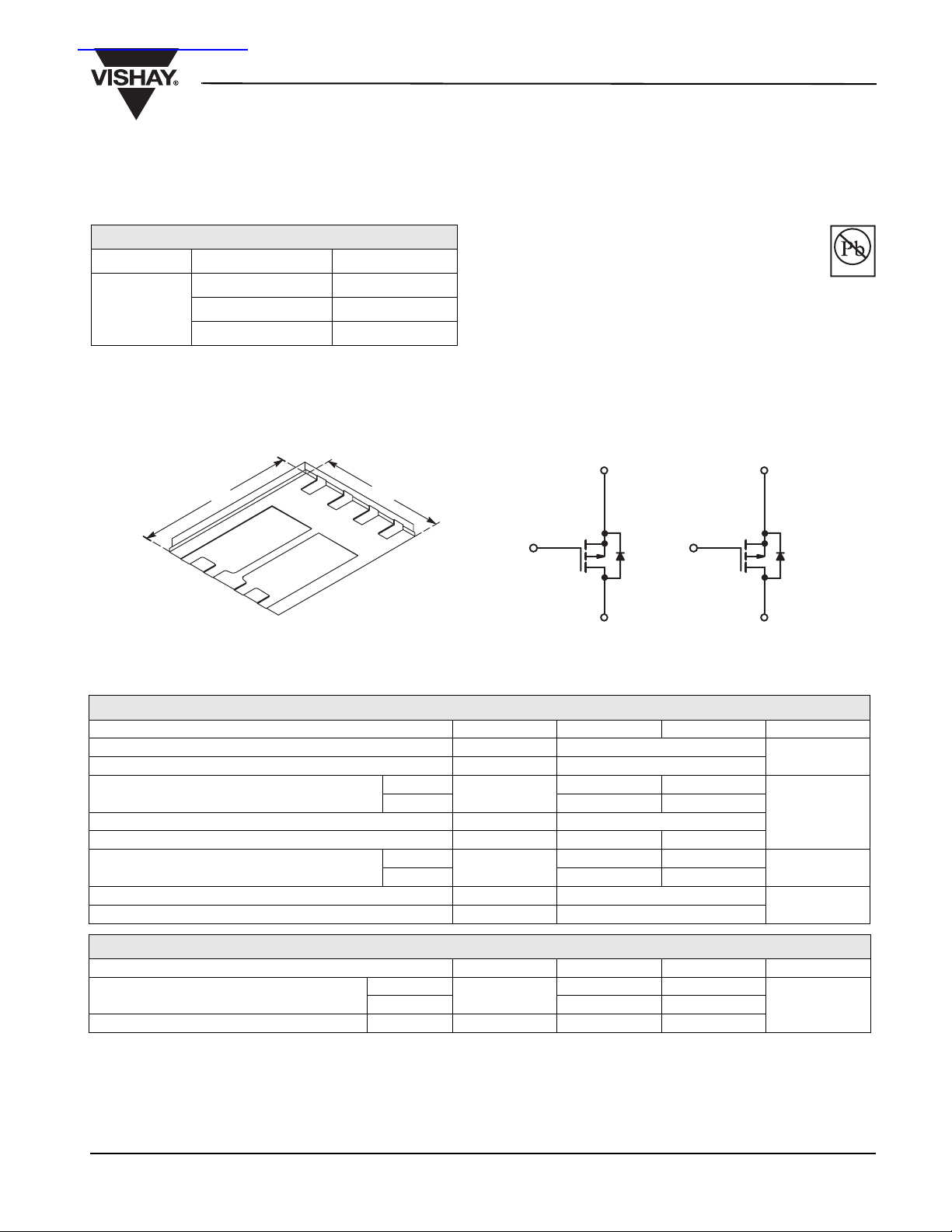
Ordering Information: Si7909DN-T1
(Ω)I
DS(on)
GS
GS
GS
PowerPAK 1212-8
D2
6
D2
5
Bottom View
Si7909DN–T1–E3 (Lead (Pb)–free)
New Product
Dual P-Channel 12-V (D-S) MOSFET
FEATURES
(A)
D
= –4.5 V –7.7
= –2.5 V –6.8
= –1.8 V –5.7
S1
1
3.30 mm
G1
2
S2
3
G2
4
•TrenchFET® Power MOSFETS: 1.8-V Rated
• New Low Thermal Resistance PowerPAK
Package
• Advanced High Cell Density Process
• Ultra-Low r
, and High PD Capability
DS(on)
APPLICATIONS
• Load Switch
• PA Switch
• Battery Switch
• Bi-Directional Switch
S
1
G
1
D
1
P-Channel MOSFET
G
Vishay Siliconix
S
2
2
D
2
P-Channel MOSFE
®
Pb-free
Available
RoHS*
COMPLIANT
ABSOLUTE MAXIMUM RATINGS TA = 25°C, unless otherwise noted
Parameter Symbol 10 secs Steady State Unit
Drain-Source Voltage V
Gate-Source Voltage V
a
TA = 25°C
T
= 85°C –5.5 –3.8
A
T
= 25°C
A
T
= 85°C 1.5 0.85
A
Continuous Drain Current (T
Pulsed Drain Current
= 150°C)
J
a
Continuous Source Current (Diode Conduction)
Maximum Power Dissipation
a
Operating Junction and Storage Temperature Range T
Soldering Recommendations (Peak Temperature)
b,c
DS
GS
I
D
I
DM
I
S
P
D
, T
J
stg
–7.7 –5.3
–2.3 –1.1
2.8 1.3
–12
±8
–20
–55 to 150
260
V
A
W
°C
THERMAL RESISTANCE RATINGS
Parameter Symbol Typical Maximum Unit
Maximum Junction-to-Ambient
a
Maximum Junction-to-Case Steady State R
Notes
a. Surface Mounted on 1“ x 1“ FR4 Board.
b. See Solder Profile (
copper (not plated) as a result of the singulation process in manufacturing. A solder fillet at the exposed copper tip cannot be guaranteed and is
not required to ensure adequate bottom side solder interconnection.
c. Rework Conditions: manual soldering with a soldering iron is not recommended for leadless components.
http://www.vishay.com/ppg?73257). The PowerPAK 1212-8 is a leadless package. The end of the lead terminal is exposed
t ≤ 10 sec
Steady State 75 94
R
thJA
thJC
* Pb containing terminations are not RoHS compliant, exemptions may apply
35 44
°C/W
45
Document Number: 71996
S-51210–Rev. C, 27-Jun-05
www.vishay.com
1
Page 2
Si7909DN
5
Vishay Siliconix
New Product
SPECIFICATIONS TJ = 25°C, unless otherwise noted
Parameter Symbol Test Condition Min Typ Max Unit
Static
V
Gate Threshold Voltage V
Gate-Body Leakage
Zero Gate Voltage Drain Current
On-State Drain Current
a
Drain-Source On-State Resistance
Forward Transconductance
Diode Forward Voltage
Dynamic
b
a
a
GS(th)
I
GSS
I
DSS
I
D(on)
a
r
DS(on)
g
fs
V
SD
V
V
Total Gate Charge Qg
Gate-Source Charge Q
Gate-Drain Charge Q
Tur n - O n D e l ay Time t
Rise Time t
Turn-Off DelayTime t
Fall Time t
Source-Drain Reverse Recovery Time t
gs
gd
d(on)
r
d(off)
f
rr
V
DS
4.3
I
90 135
D
Notes
a. Pulse test; pulse width ≤ 300 µs, duty cycle ≤ 2 %.
b. Guaranteed by design, not subject to production testing.
= VGS, ID = –700 µA –0.40 –1.0 V
DS
VDS = 0 V, VGS = ±8 V ±100
V
= –12 V, VGS = 0 V –1
DS
= –12 V, V
DS
≤ –5 V, V
DS
V
= –4.5 V, ID = –7.7 A 0.031 0.037
GS
= –2.5 V, ID = –6.8 A 0.040 0.048
V
GS
V
= –1.8 V, ID = –3.0 A 0.057 0.068
GS
V
= –6 V, ID = –7.7 A 17 S
DS
IS = –2.3 A, VGS = 0 V –0.7 –1.2 V
= –6 V, V
≅ –1 A, V
GS
V
= –6 V, RL = 6 Ω
DD
GEN
IF = –2.3 A, di/dt = 100 A/µs 70 110
= 0 V, TJ = 85°C –5
GS
= –4.5 V –20 A
GS
15.5 24
= –4.5 V, ID = –7.7 A
2.5
25 40
45 70
= –4.5 V, RG = 6 Ω
85 130
nA
µA
Ω
nC
ns
Stresses beyond those listed under “Absolute Maximum Ratings” may cause permanent damage to the device. These are stress ratings only, and functional operation
of the device at these or any other conditions beyond those indicated in the operational sections of the specifications is not implied. Exposure to absolute maximum
rating conditions for extended periods may affect device reliability.
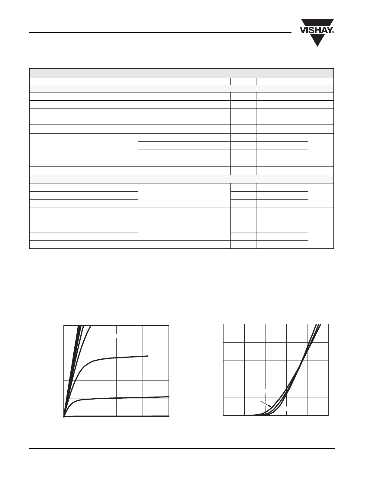
TYPICAL CHARACTERISTICS TA = 25°C, unless otherwise noted
20
VGS = 5 thru 2.5 V
16
2 V
12
8
– Drain Current (A)I
D
4
0
01234
– Drain-to-Source Voltage (V)
V
DS
Output Characteristics
1.5 V
1 V
20
16
12
8
– Drain Current (A)I
D
4
0
0.0 0.5 1.0 1.5 2.0 2.
TC = 125˚C
25˚C
–55˚C
– Gate-to-Source Voltage (V)
V
GS
Transfer Characteristics
www.vishay.com
2
Document Number: 71996
S-51210–Rev. C, 27-Jun-05
Page 3

Si7909DN
New Product
TYPICAL CHARACTERISTICS TA = 25°C, unless otherwise noted
2400
1800
1200
C – Capacitance (pF)
600
0
1.3
1.2
)
– On-Resistance (Ωr
DS(on)
0.12
0.09
VGS = 1.8 V
0.06
0.03
0.00
048121620
I
– Drain Current (A)
D
VGS = 2.5 V
VGS = 4.5 V
On-Resistance vs. Drain Current
5
VDS = 6 V
= 7.7 A
I
D
4
Vishay Siliconix
C
iss
C
oss
C
rss
024681012
VDS – Drain-to-Source Voltage (V)
Capacitance
VGS = 4.5 V
= 7.7 A
I
D
– Gate-to-Source Voltage (V)
GS
V
– Source Current (A)I
S
3
2
1
0
048121620
Qg – Total Gate Charge (nC)
Gate Charge
20
10
TJ = 150˚C
TJ = 25˚C
1.1
(Normalized)
1.0
(on) – On–Resistance
DS
r
0.9
0.8
–50 –25 0 25 50 75 100 125 150
– Junction Temperature (˚C)
T
J
On-Resistance vs. Junction Temperature
0.12
0.10
)
ID = 7.7 A
– On-Resistance (Ωr
DS(on)
0.08
0.06
0.04
0.02
ID = 3 A
1
0.0 0.2 0.4 0.6 0.8 1.0 1.2
VSD – Source-to-Drain Voltage (V)
Source-Drain Diode Forward Voltage
Document Number: 71996
S-51210–Rev. C, 27-Jun-05
0.00
012345
VGS – Gate-to-Source Voltage (V)
On-Resistance vs. Gate-to-Source Voltage
www.vishay.com
3
Page 4

Si7909DN
)
q
)
Vishay Siliconix
New Product
TYPICAL CHARACTERISTICS TA = 25°C, unless otherwise noted
0.4
0.3
ID = 700 µA
0.2
0.1
Variance (V)V
GS(th)
0.0
–0.1
–0.2
–50 –25 0 25 50 75 100 125 150
TJ – Temperature (˚C)
Threshold Voltage
100
r
DS(on)
Limited
50
40
30
Power (W)
20
10
I
Limited
DM
0
0.1 60010.010.001
10 100
Time (sec
Single Pulse Power, Juncion-To-Ambient
2
1
0.1
Thermal Impedance
Normalized Effective Transient
0.01
10
Duty Cycle = 0.5
0.2
0.1
0.05
0.02
–4
10
P(t) = 0.001
1
I
D(on)
Limited
– Drain Current (A)I
D
0.1
TA = 25˚C
Single Pulse
BV
DSS
Limited
P(t) = 0.01
P(t) = 0.1
P(t) = 1
P(t) = 10
dc
0.01
0.1 1 10 100
VDS – Drain-to-Source Voltage (V)
Safe Operating Area, Junction-To-Ambient
Single Pulse
–3
10
–2
10
S
–1
1 10 60010
uare Wave Pulse Duration (sec
Normalized Thermal Transient Impedance, Junction-to-Ambient
Notes:
P
DM
t
1
t
– TA = PDMZ
JM
2
1. Duty Cycle, D =
2. Per Unit Base = R
3. T
4. Surface Mounted
thJA
thJA
100
t
1
t
2
= 65˚C/W
(t)
www.vishay.com
4
Document Number: 71996
S-51210–Rev. C, 27-Jun-05
Page 5
Si7909DN
New Product
TYPICAL CHARACTERISTICS TA = 25°C, unless otherwise noted
2
1
Duty Cycle = 0.5
0.2
0.02
0.05
0.1
–3
10
Square Wave Pulse Duration (sec)
–2
10
Normalized Thermal Transient Impedance, Junction-to-Case
0.1
Thermal Impedance
Normalized Effective Transient
0.01
10
Single Pulse
–4
Vishay Siliconix
–1
110
Vishay Siliconix maintains worldwide manufacturing capability. Products may be manufactured at one of several qualified locations. Reliability data for Silicon Technology and Package Reliability represent a composite of all qualified locations. For related documents such as package/tape drawings, part marking, and reliability
data, see http://www.vishay.com/ppg?71996.
Document Number: 71996
www.vishay.com
S-51210–Rev. C, 27-Jun-05
5
 Loading...