

Vishay Siliconix
T
N-Channel 30-V (D-S) Fast Switching MOSFET
Si7840BDP
PRODUCT SUMMARY
VDS (V) R
0.0085 at V
30
0.0105 at V
(Ω)I
DS(on)
= 10 V
GS
= 4.5 V
GS
(A) Qg (Typ.)
D
16.5
13
14
FEATURES
• Halogen-free According to IEC 61249-2-21
Available
• TrenchFET
• New Low Thermal Resistance PowerPAK
®
Power MOSFET
®
Package with Low 1.07 mm Profile
• 100 % R
PowerP AK SO-8
Tested
g
APPLICATIONS
• DC/DC Converters
• Optimized for “High-Side” Synchronous Rectifier
Operations
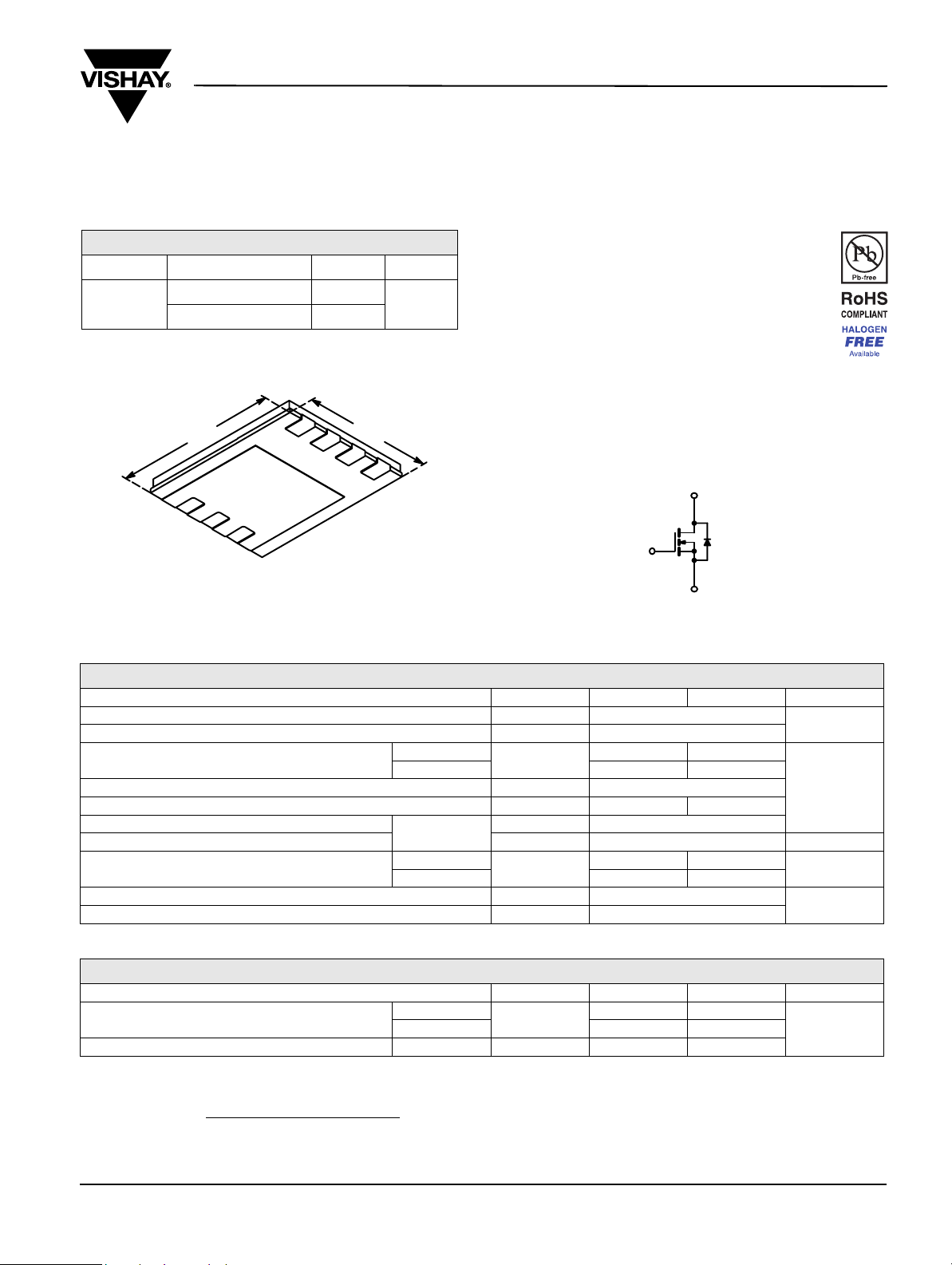
D
G
S
N-Channel MOSFE
6.15 mm
D
8
Ordering Information:
S
1
D
7
D
6
D
5
Bottom View
Si7840BDP-T1-E3 (Lead (Pb)-free)
Si7840BDP-T1-GE3 (Lead (Pb)-free and Halogen-free)
5.15 mm
S
2
S
3
G
4
ABSOLUTE MAXIMUM RATINGS TA = 25 °C, unless otherwise noted
Parameter Symbol 10 s Steady State Unit
Drain-Source Voltage
Gate-Source Voltage
Continuous Drain Current (T
= 150°C)
J
a
Pulsed Drain Current
Continuous Source Current (Diode Conduction)
a
Avalanche Current
Avalanche Energy
Maximum Power Dissipation
a
Operating Junction and Storage Temperature Range
Soldering Recommendations (Peak Temperature)
c, d
TA = 25 °C
= 70 °C
T
A
L = 0.1 mH
TA = 25 °C
= 70 °C
T
A
V
DS
V
GS
I
D
I
DM
I
S
I
AS
E
AS
P
D
, T
T
J
stg
16.5 11
13 8
3.7 1.6
4.1 1.8
2.6 1.1
30
± 20
50
20
20 mJ
- 55 to 150
260
V
A
W
°C
THERMAL RESISTANCE RATINGS
Parameter Symbol Typical Maximum Unit
Maximum Junction-to-Ambient
a
Maximum Junction-to-Case (Drain) Steady State
t ≤ 10 s
R
thJA
R
thJC
Notes:
a. Surface Mounted on 1" x 1" FR4 board.
b. t = 10 s.
c. See Solder Profile (http://www.vishay.com/ppg?73257
). The PowerPAK SO-8 is a leadless package. The end of the lead terminal is exposed
copper (not plated) as a result of the singulation process in manufacturing. A solder fillet at the exposed copper tip cannot be guaranteed and
is not required to ensure adequate bottom side solder interconnection.
d. Rework Conditions: manual soldering with a soldering iron is not recommended for leadless components.
Document Number: 73218
S09-0272-Rev. C, 16-Feb-09
23 30
°C/WSteady State 60 70
3.1 3.6
www.vishay.com
1
Si7840BDP
0
Vishay Siliconix
MOSFET SPECIFICATIONS TJ = 25 °C, unless otherwise noted
Parameter Symbol Test Condition Min. Typ. Max. Unit
Static
V
Gate Threshold Voltage
Gate-Body Leakage
Zero Gate Voltage Drain Current
On-State Drain Current
Drain-Source On-State Resistance
Forward Transconductance
Diode Forward Voltage
Dynamic
b
a
a
a
a
Total Gate Charge
Gate-Drain Charge
Gate Resistance
Tur n -O n De l ay Ti m e
Rise Time
Turn-Off Delay Time
Fall Time
Source-Drain Reverse Recovery Time
Reverse Recovery Charge
V
GS(th)
I
GSS
I
DSS
I
V
D(on)
R
DS(on)
g
fs
V
SD
Q
g
Q
gs
Q
gd
R
g
t
d(on)
t
r
t
d(off)
t
f
t
rr
Q
rr
V
V
DS
I
Notes:
a. Pulse test; pulse width ≤ 300 µs, duty cycle ≤ 2 %.
b. Guaranteed by design, not subject to production testing.
Stresses beyond those listed under “Absolute Maximum Ratings” may cause permanent damage to the de vice. These are stress rating s only, and functiona l operation
of the device at these or any other conditions beyond those indicated in the operational sections of the specifications is not implied. Exposure to absolute maximum
rating conditions for extended periods may affect device reliability.
= VGS, ID = 250 µA
DS
VDS = 0 V, VGS = ±20 V
V
= 30 V, V
DS
= 30 V, V
DS
≥ 5 V, V
DS
V
= 10 V, ID = 16.5 A
GS
V
= 4.5 V, ID = 13 A
GS
= 0 V
GS
= 0 V, TJ = 55°C
GS
= 10 V
GS
VDS = 15 V, ID = 16.5 A
IS = 3.7 A, V
= 15 V, V
V
= 15 V, RL = 15 Ω
DD
≅ 1 A, V
D
GS
GEN
= 0 V
GS
= 4.5 V, ID = 16.5 A
= 10 V, Rg = 6 Ω
IF = 4.1 A, dI/dt = 100 A/µs
1.0 3.0 V
±100 nA
1
10
µA
30 A
0.007 0.0085
0.0084 0.0105
60 S
0.75 1.1 V
14 21
6
nCGate-Source Charge
3.5
0.2 0.7 1.2 Ω
17 26
14 21
39 60
14 21
26 40
20 nC
Ω
ns
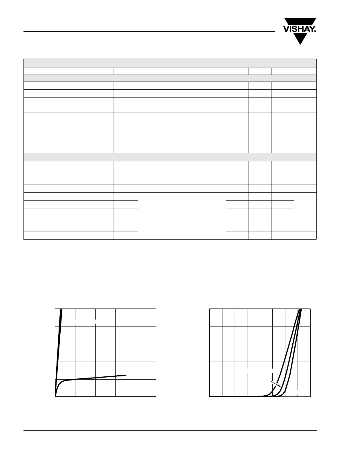
TYPICAL CHARACTERISTICS 25 °C, unless otherwise noted
40
32
24
16
- Drain Current (A)I
D
8
0
www.vishay.com
2
VGS = 10 thru 4 V
3 V
012345
V
- Drain-to-Source Voltage (V)
DS
Output Characteristics
- Drain Current (A)I
D
50
40
30
20
TC = 125˚C
10
0
0.0 0.5 1.0 1.5 2.0 2.5 3.0 3.5 4.
V
- Gate-to-Source Voltage (V)
GS
25˚C
-55˚C
Transfer Characteristics
Document Number: 73218
S09-0272-Rev. C, 16-Feb-09
TYPICAL CHARACTERISTICS 25 °C, unless otherwise noted
0
Si7840BDP
Vishay Siliconix
0.012
0.011
Ω)
0.010
0.009
0.008
On-Resistance (R
-
0.007
DS(on)
0.006
0.005
0.004
- Gate-to-Source Voltage (V)
GS
V
VGS = 4.5 V
VGS = 10 V
0 5 10 15 20 25 30 35 40
ID - Drain Current (A)
On-Resistance vs. Drain Current
6
VDS = 15 V
5
4
3
2
1
= 16.5 A
I
D
2500
2000
1500
1000
Capacitance (pF)
-
C
500
0
0 5 10 15 20 25 3
1.8
1.6
1.4
1.2
- On-Resistance
(Normalized)
1.0
DS(on)
R
0.8
C
iss
C
oss
C
rss
VDS - Drain-to-Source Voltage (V)
Capacitance
VGS = 10 V
= 16.5 A
I
D
0
0 2 4 6 8 10121416
40
10
- Source Current (A)I
S
1
0.0 0.2 0.4 0.6 0.8 1.0 1.2
TJ = 150˚C
VSD - Source-to-Drain Voltage (V)
Source-Drain Diode Forward Voltage
Document Number: 73218
S09-0272-Rev. C, 16-Feb-09
Qg - Total Gate Charge (nC)
Gate Charge
TJ = 25˚C
0.6
- 50 - 25 0 25 50 75 100 125 150
TJ- Junction Temperature (°C)
On-Resistance vs. Junction Temperature
0.05
0.04
)
Ω
ID = 16.5 A
0.03
0.02
- On-Resistance (R
DS(on)
0.01
0.00
0246810
VGS - Gate-to-Source Voltage (V)
On-Resistance vs. Gate-to-Source Voltage
www.vishay.com
3
Si7840BDP
Vishay Siliconix
TYPICAL CHARACTERISTICS 25 °C, unless otherwise noted
0.4
0.2
-0.0
ID = 250 μA
-0.2
Variance (V)V
-0.4
GS(th)
-0.6
-0.8
-1.0
-50 - 25 0 25 50 75 100 125 150
TJ - Temperature (˚C)
Threshold Voltage
100
Limited by R
Drain Current (A)I
-
D
DS(on)*
10
1
0.1
TC = 25 °C
Single Pulse
Power (W)
50
40
30
20
10
0
0.001
1 ms
10 ms
100 ms
1 s
10 s
dc
1
10 6000.1
Time (s)
Single Pulse Power
1000.01
0.1
Thermal Impedance
Normalized Effective Transient
0.01
www.vishay.com
4
2
1
Duty Cycle = 0.5
0.2
0.1
0.05
0.02
-
4
10
Single Pulse
0.01
0.1 1 10 100
- Drain-to-Source Voltage (V)
V
DS
> minimum VGS at which R
* V
GS
DS(on)
is specified
Safe Operating Area, Junction-to-Case
Notes:
P
DM
t
1
t
2
t
thJA
thJA
100
1
t
2
= 58°C/W
(t)
1. Duty Cycle, D =
2. Per Unit Base = R
3. T
- TA = PDMZ
JM
4. Surface Mounted
-
3
10
-
2
10
-
1
Square Wave Pulse Duration (s)
1 10 60010
Normalized Thermal Transient Impedance, Junction-to-Ambient
Document Number: 73218
S09-0272-Rev. C, 16-Feb-09
 Loading...