

30
36
查询SI7336DP供应商
PRODUCT SUMMARY
V
(V) r
DS
0.00325 @ VGS = 10 V 30
0.0042 @ VGS = 4.5 V 27
DS(on)
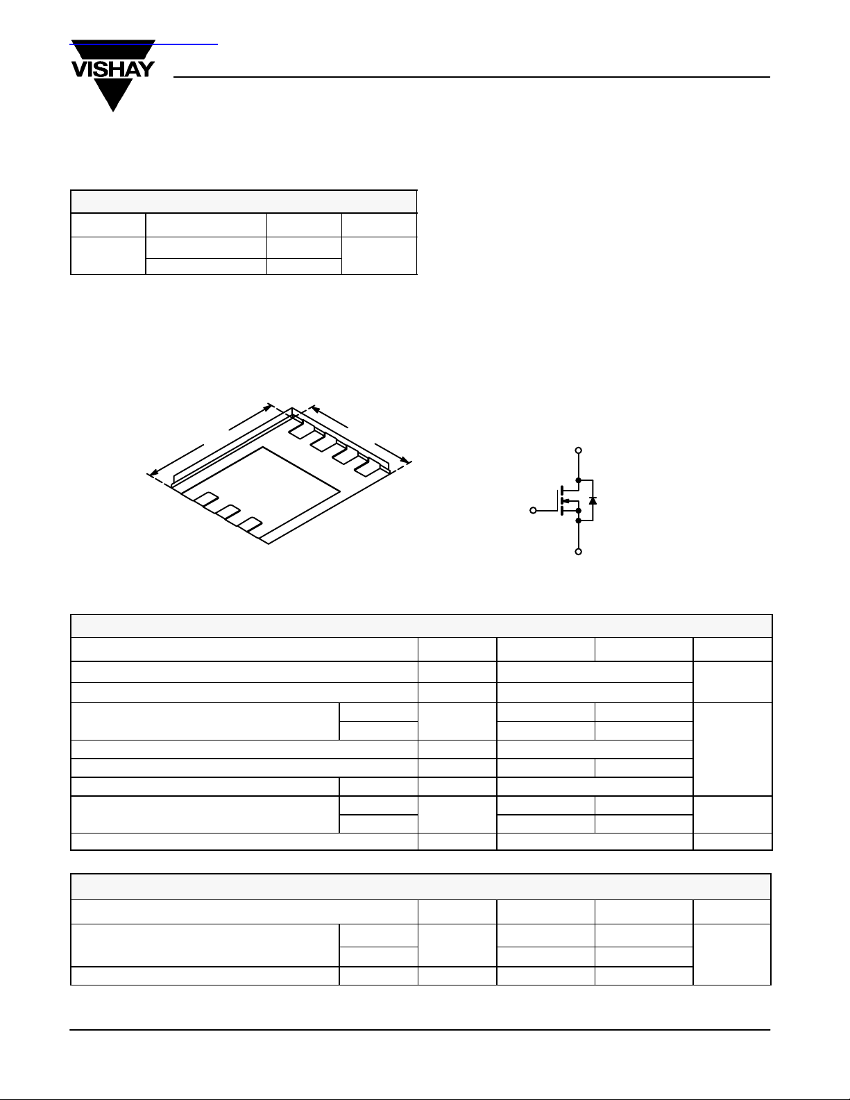
N-Channel 30-V (D-S) MOSFET
(W) I
PowerPAK SO-8
(A) Qg (T yp)
D
Si7336DP
Vishay Siliconix
FEATURES
D Ultra-Low On-Resistance Using High Density
TrenchFETr Gen II Power MOSFET Technology
D Qg Optimized
D New Low Thermal Resistance PowerPAKr Package
with Low 1.07-mm Profile
D 100% R
APPLICATIONS
D Low-Side DC/DC Conversion
− Notebook
− Server
− Workstation
D Synchronous Rectifier, POL
Tested
g
6.15 mm
D
8
D
7
D
6
5
Bottom View
Ordering Information: Si7336DP-T1
S
1
D
5.15 mm
S
2
S
3
G
4
G
N-Channel MOSFET
D
S
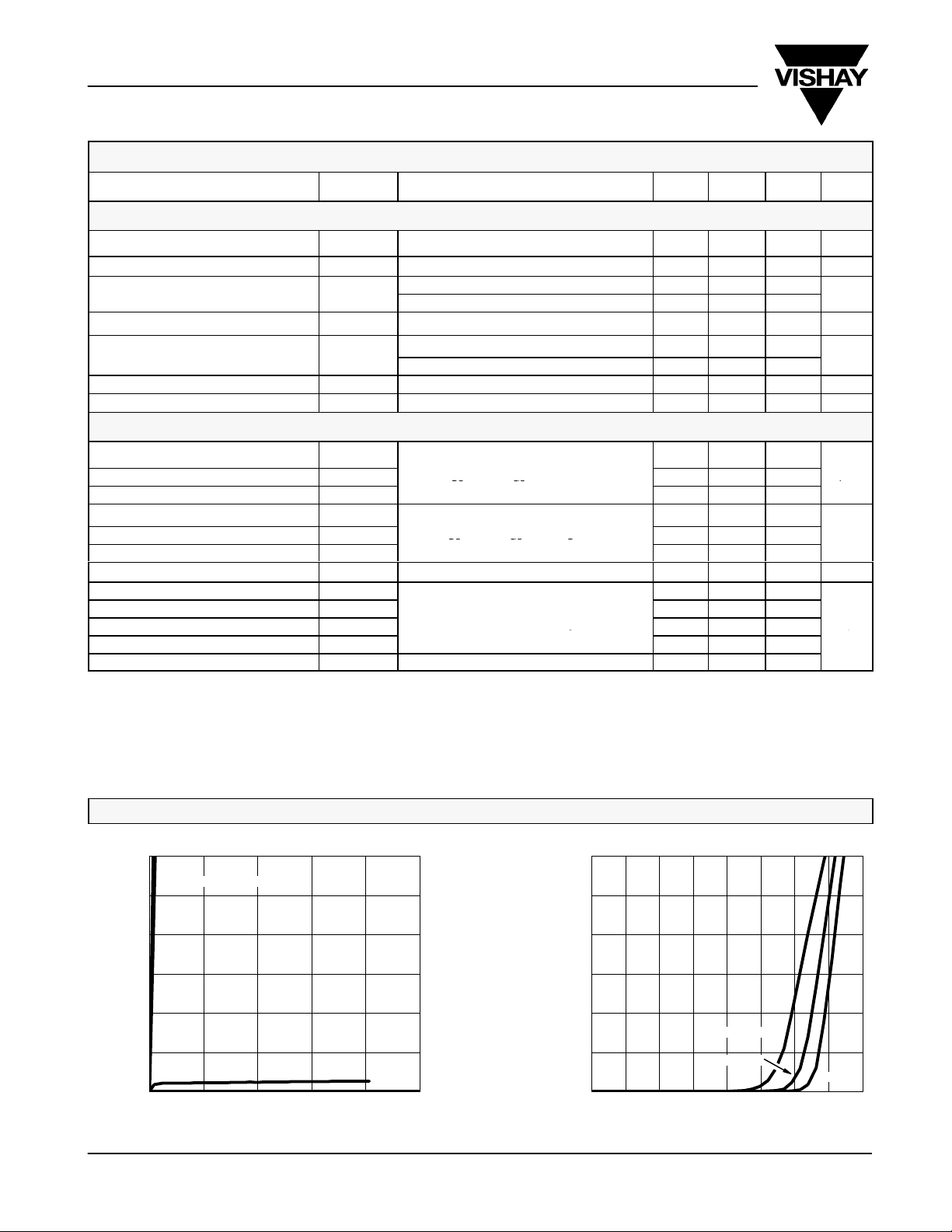
ABSOLUTE MAXIMUM RATINGS (TA = 25_C UNLESS OTHERWISE NOTED)
Parameter Symbol 10 secs Steady State Unit
Drain-Source Voltage V
Gate-Source Voltage V
a
Continuous Drain Current (TJ = 150_C)
Pulsed Drain Current (10 ms Pulse Width) I
Continuous Source Current (Diode Conduction)
Avalanche Current L = 1.0 mH I
Maximum Power Dissipation
Operating Junction and Storage Temperature Range TJ, T
_
a
a
TA = 25_C
TA = 70_C
TA = 25_C
TA = 70_C
P
I
DM
I
AS
DS
GS
D
S
D
stg
30 18
25 15
4.5 1.8
5.4 1.9
3.4 1.2
30
"20
70
50
−55 to 150 _C
V
A
W
THERMAL RESISTANCE RATINGS
Maximum Junction-to-Ambient
Maximum Junction-to-Case (Drain) Steady State R
Notes
a. Surface Mounted on 1” x 1” FR4 Board.
Document Number: 72415
S-41795—Rev. C, 04-Oct-04
Parameter Symbol Typical Maximum Unit
a
t v 10 sec
Steady State
R
thJA
thJC
18 23
50 65
1.0 1.5
www.vishay.com
_C/W
1
Si7336DP
Drain-S
a
W
DS
,
GS
,
p
DS
,
GS
,
D
VDD = 15 V, RL = 15 W
g
ns
Vishay Siliconix
MOSFET SPECIFICATIONS (TJ = 25_C UNLESS OTHERWISE NOTED)
Parameter Symbol T est Condition Min Typ Max Unit
Static
Gate Threshold Voltage V
Gate-Body Leakage I
Zero Gate Voltage Drain Current I
On-State Drain Current
-
ource On-State Resistance
Forward Transconductance
Diode Forward Voltage
Dynamic
b
a
-
a
a
a
Input Capacitance C
Output Capacitance C
Reverse Transfer Capacitance C
Total Gate Charge Q
Gate-Source Charge Q
Gate-Drain Charge Q
Gate Resistance R
Turn-On Delay Time t
Rise Time t
Turn-Off Delay Time t
Fall Time t
Source-Drain Reverse Recovery Time t
Notes
a. Pulse test; pulse width v
b. Guaranteed by design, not subject to production testing.
300 ms, duty cycle v 2%.
GS(th)
GSS
DSS
I
D(on)
r
DS(on)
g
V
d(on)
d(off)
fs
SD
iss
oss
rss
g
gs
gd
g
r
f
rr
VDS = VGS, I
= 250 mA 1.0 3.0 V
D
VDS = 0 V, VGS = "20 V "100 nA
VDS = 30 V, VGS = 0 V 1
VDS = 30 V, VGS = 0 V, TJ = 55_C 5
VDS w 5 V, VGS = 10 V
VGS = 10 V, ID = 25 A
30 A
0.0026 0.00325
VGS = 4.5 V, ID = 19 A 0.0033 0.0042
VDS = 15 V, ID = 25 A 110 S
IS = 2.9 A, VGS = 0 V 0.72 1.1 V
5600
V
= 15 V, VGS = 0 V, f = 1 MHz 860 pF
DS
415
36 50
V
= 15 V, VGS = 4.5 V, ID = 20 A 18 nC
DS
10
0.8 1.3 2.0 W
24 35
VDD = 15 V, RL = 15 W
ID ^ 1 A, V
GEN
= 10 V, Rg = 6 W
16 25
90 140
32 50
IF = 2.9 A, di/dt = 100 A/ms 45 70
mA
ns
Stresses beyond those listed under “Absolute Maximum Ratings” may cause permanent damage to the device. These are stress ratings only, and functional operation
of the device at these or any other conditions beyond those indicated in the operational sections of the specifications is not implied. Exposure to absolute maximum rating
conditions for extended periods may affect device reliability.
TYPICAL CHARACTERISTICS (25_C UNLESS NOTED)
Output Characteristics Transfer Characteristics
VGS = 10 thru 4 V
3 V
VDS − Drain-to-Source Voltage (V)
− Drain Current (A)I
D
www.vishay.com
2
60
50
40
30
20
10
0
0246810
60
50
40
30
20
− Drain Current (A)I
D
10
TC = 125_C
25_C
0
0.0 0.5 1.0 1.5 2.0 2.5 3.0 3.5 4.0
VGS − Gate-to-Source Voltage (V)
Document Number: 72415
S-41795—Rev. C, 04-Oct-04
−55_C
TYPICAL CHARACTERISTICS (25_C UNLESS NOTED)
Si7336DP
Vishay Siliconix
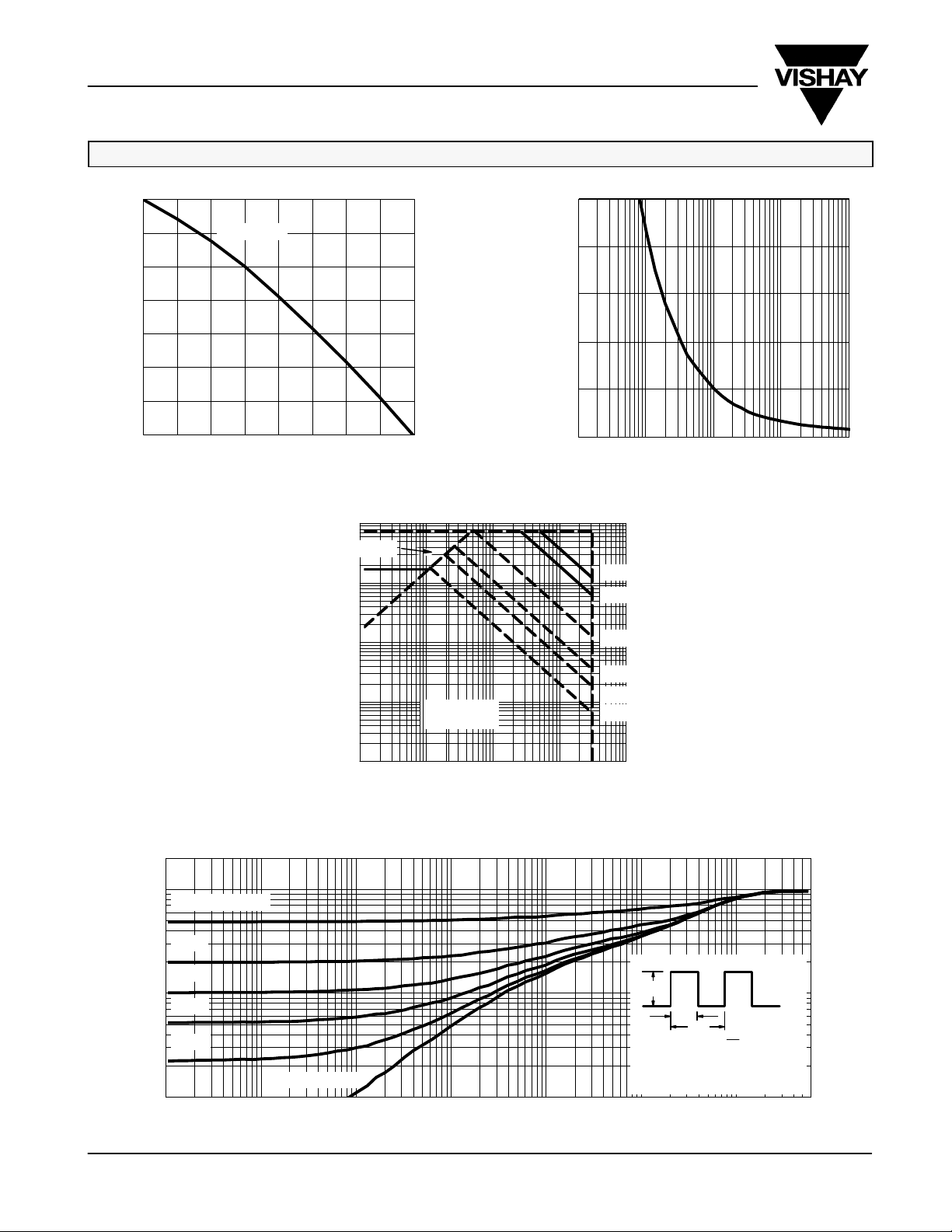
0.005
0.004
W )
0.003
0.002
− On-Resistance (r
DS(on)
0.001
0.000
− Gate-to-Source Voltage (V)
GS
V
On-Resistance vs. Drain Current
VGS = 4.5 V
VGS = 10 V
0 1020304050
ID − Drain Current (A)
6
5
4
3
2
1
VDS = 15 V
I
= 20 A
D
Gate Charge
7000
6000
5000
4000
3000
C − Capacitance (pF)
2000
1000
0
0 6 12 18 24 30
On-Resistance vs. Junction Temperature
1.6
1.4
1.2
1.0
− On-Resiistance
(Normalized)
DS(on)
r
0.8
Capacitance
C
C
rss
V
DS
VGS = 10 V
I
= 25 A
D
oss
− Drain-to-Source Voltage (V)
C
iss
0
0 5 10 15 20 25 30 35 40 45
Source-Drain Diode Forward Voltage On-Resistance vs. Gate-to-Source Voltage
50
10
− Source Current (A)I
S
Document Number: 72415
S-41795—Rev. C, 04-Oct-04
1
0.1
0.00 0.2 0.4 0.6 0.8
VSD − Source-to-Drain Voltage (V) VGS − Gate-to-Source Voltage (V)
Qg − Total Gate Charge (nC)
TJ = 150_C
TJ = 25_C
1.0 1.2
W )
− On-Resistance (r
DS(on)
0.6
−50 −25 0 25 50 75 100 125 150
T
− Junction Temperature (_C)
J
0.015
0.012
0.009
0.006
0.003
0.000
0246810
ID = 25 A
www.vishay.com
3
Si7336DP
Vishay Siliconix
TYPICAL CHARACTERISTICS (25_C UNLESS NOTED)
0.4
Threshold Voltage
0.2
−0.0
−0.2
Variance (V)V
−0.4
GS(th)
−0.6
−0.8
−1.0
−50 −25 0 25 50 75 100 125 150
ID = 250 mA
TJ − Temperature (_C)
Limited by r
Safe Operating Area, Junction-to-Case
100
*
DS(on)
10
200
160
120
Power (W)
80
40
0
Single Pulse Power
1100.10.010.001
Time (sec)
1 ms
10 ms
2
1
0.1
Thermal Impedance
Normalized Effective Transient
0.01
−4
10
Duty Cycle = 0.5
0.2
0.1
0.05
0.02
10
1
0.1
TC = 25_C
Single Pulse
0.01
0.01 1 10 100
0.1
VDS − Drain-to-Source Voltage (V)
*V
u minimum VGS at which r
GS
DS(on)
is specified
Normalized Thermal Transient Impedance, Junction-to-Ambient
Single Pulse
−3
−2
10
−1
1 10 60010
Square Wave Pulse Duration (sec)
100 ms
1 s
10 s
dc
Notes:
P
1. Duty Cycle, D =
2. Per Unit Base = R
3. TJM − TA = PDMZ
4. Surface Mounted
DM
t
1
t
2
t
1
t
2
= 50_C/W
thJA
(t)
thJA
100
www.vishay.com
4
Document Number: 72415
S-41795—Rev. C, 04-Oct-04
TYPICAL CHARACTERISTICS (25_C UNLESS NOTED)
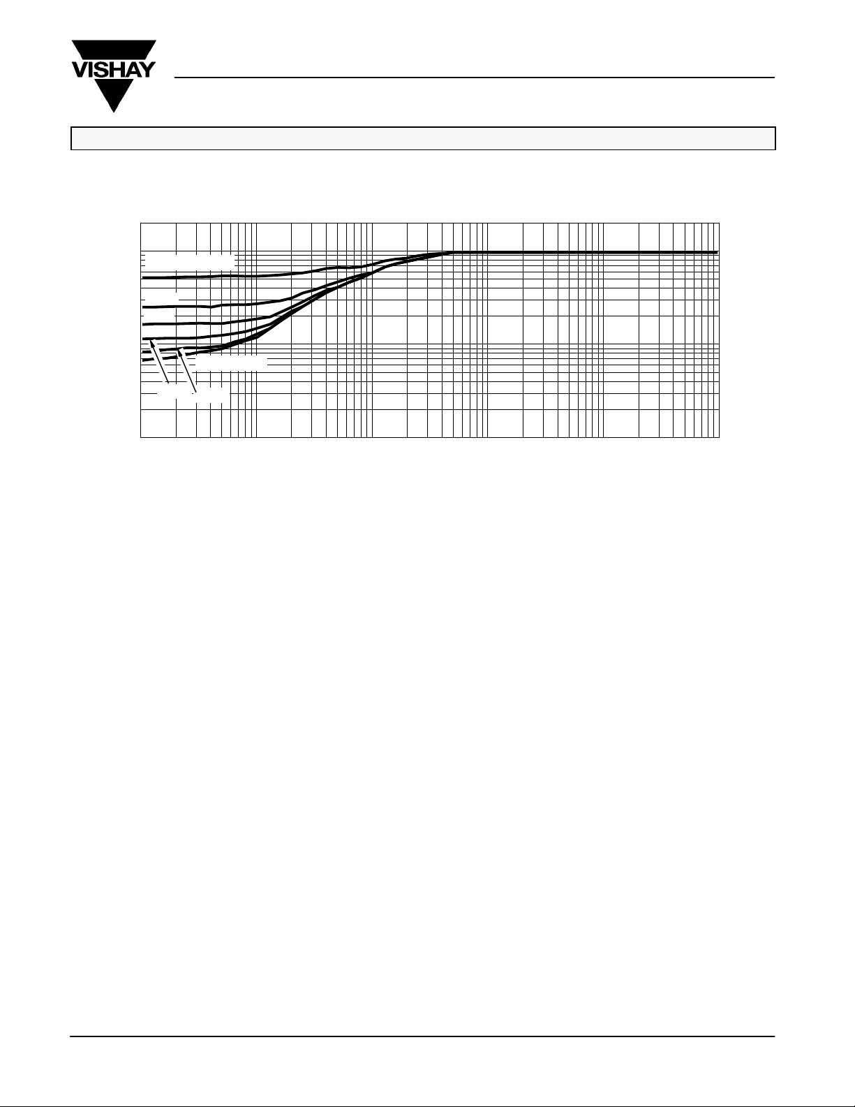
Normalized Thermal Transient Impedance, Junction-to-Case
2
1
Duty Cycle = 0.5
0.2
0.1
0.1
Thermal Impedance
Normalized Effective Transient
0.05
Single Pulse
0.02
Si7336DP
Vishay Siliconix
0.01
−4
10
−3
10
−2
10
Square Wave Pulse Duration (sec)
−1
11010
Vishay Siliconix maintains worldwide manufacturing capability. Products may be manufactured at one of several qualified locations. Reliability data for Silicon Technology
and Package Reliability represent a composite of all qualified locations. For related documents such as package/tape drawings, part marking, and reliability data, see
http://www.vishay.com/ppg?72415.
Document Number: 72415
S-41795—Rev. C, 04-Oct-04
www.vishay.com
5
 Loading...