

Vishay si4932dy Datasheet
Dual N-Channel 30-V (D-S) MOSFET
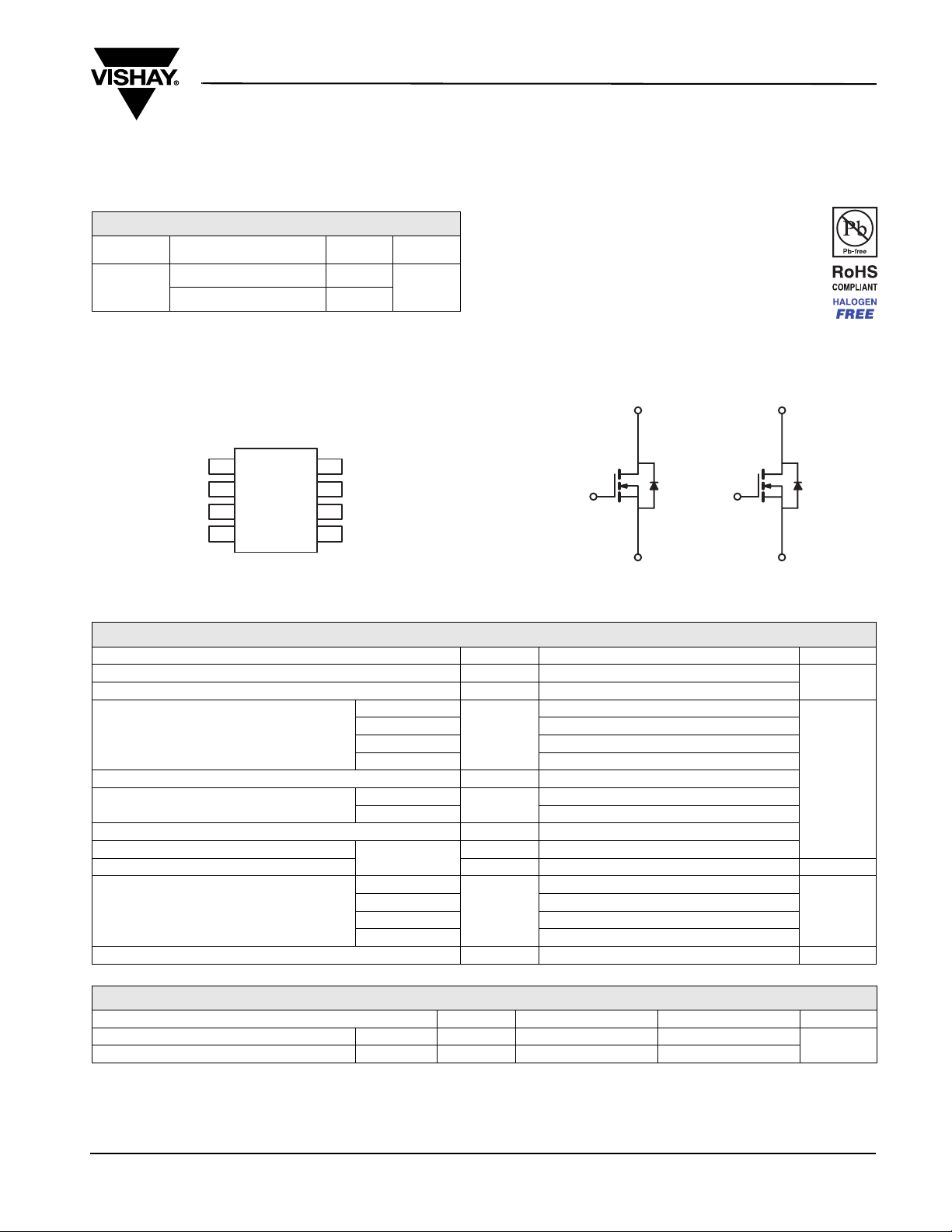
Si4932DY
Vishay Siliconix
PRODUCT SUMMARY
VDS (V) R
0.015 at V
30
0.017 at V
DS(on)
(Ω)
GS
GS
= 10 V
= 4.5 V
a, e
I
(A)
D
Qg (Typ.)
8
8
14.7
• Halogen-free According to IEC 61249-2-21
•TrenchFET® Power MOSFET
• 100 % R
Tested
g
• 100 % UIS Tested
APPLICATIONS
FEATURES
• DC/DC Conversion
• Load Switching
D
2
S
2
N-Channel MOSFET
SO-8
S
1
1
G
2
1
S
3
2
G
4
2
Top View
Ordering Information: Si4932DY-T1-GE3 (Lead (Pb)-free and Halogen-free)
D
8
1
D
7
1
D
6
2
D
5
2
D
1
G
1
S
1
N-Channel MOSFET
G
2
ABSOLUTE MAXIMUM RATINGS TA = 25 °C, unless otherwise noted
Parameter Symbol Limit Unit
Drain-Source Voltage
Gate-Source Voltage
T
Continuous Drain Current (T
= 150 °C)
J
T
TA = 25 °C
TA = 70 °C
Pulsed Drain Current (10 µs Pulse Width)
Source-Drain Current Diode Current
T
T
Pulsed Source-Drain Current
Single Pulse Avalanche Current
Single Pulse Avalanche Energy
L = 0.1 mH
T
Maximum Power Dissipation
T
T
TA = 70 °C
Operating Junction and Storage Temperature Range
= 25 °C
C
= 70 °C
C
= 25 °C
C
= 25 °C
A
= 25 °C
C
= 70 °C
C
= 25 °C
A
V
DS
V
GS
I
D
I
DM
I
S
I
SM
I
AS
E
AS
± 20
b, c, e
8
6.8
1.7
30
8
8
30
2.6
30
20
20
V
e
e
b, c
A
b, c
mJ
3.2
P
D
T
, T
J
stg
2.1
b, c
2
b, c
1.28
- 55 to 150
W
°C
THERMAL RESISTANCE RATINGS
Parameter Symbol Typical Maximum Unit
Maximum Junction-to-Ambient
Maximum Junction-to-Foot (Drain) Steady State
Notes:
a. Based on T
b. Surface Mounted on 1" x 1" FR4 board.
= 25 °C.
C
c. t = 10 s.
d. Maximum under Steady State conditions is 110 °C/W.
e. Package limited.
Document Number: 69012
S-83042-Rev. A, 22-Dec-08
b, d
t ≤ 10 s
R
thJA
R
thJF
47 62.5
28 38
°C/W
www.vishay.com
1
Si4932DY
Vishay Siliconix
SPECIFICATIONS TJ = 25 °C, unless otherwise noted
Parameter Symbol Test Conditions Min. Typ. Max. Unit
Static
Drain-Source Breakdown Voltage
V
Temperature Coefficient ΔVDS/T
DS
V
Temperature Coefficient ΔV
GS(th)
Gate Threshold Voltage
Gate Body Leakage
Zero Gate Voltage Drain Current
On-State Drain Current
Drain-Source On-State Resistance
Forward Transconductance
Dynamic
a
b
b
b
Input Capacitance
Reverse Transfer Capacitance
Total Gate Charge
Gate-Source Charge
Gate-Drain Charge
Gate Resistance
Tur n - O n D e l ay Time
Rise Time
Turn-Off Delay Time
Fall Ti me
Tur n - O n D e l ay Time
Rise Time
Turn-Off Delay Time
Fall Ti me
V
DS
J
GS(th)/TJ
V
GS(th)
I
GSS
I
DSS
I
V
D(on)
R
DS(on)
g
fs
C
iss
C
oss
C
rss
Q
g
Q
gs
Q
gd
R
g
t
d(on)
t
r
t
d(off)
t
f
t
d(on)
t
r
t
d(off)
t
f
Drain-Source Body Diode Characteristics
Continuous Source-Drain Diode Current
Pulse Diode Forward Current
a
Body Diode Voltage
Body Diode Reverse Recovery Time
Body Diode Reverse Recovery Charge
Reverse Recovery Fall Time
Reverse Recovery Rise Time
I
S
I
SM
V
SD
t
rr
Q
rr
t
a
t
b
Notes:
a. Guaranteed by design, not subject to production testing.
b. Pulse test; pulse width ≤ 300 µs, duty cycle ≤ 2 %
V
= 0 V, ID = 250 µA
GS
ID = 250 µA
V
DS
VDS = V
V
DS
V
DS
= 30 V, V
DS
V
V
V
, ID = 250 µA
GS
= 0 V, V
GS
= 30 V, V
= 0 V, TJ = 55 °C
GS
= 5 V, V
GS
= 10 V, ID = 7 A
GS
= 4.5 V, ID = 5 A
GS
= 15 V, ID = 7 A
DS
= ± 20 V
= 0 V
GS
= 10 V
N-Channel
V
DS
V
DS
= 15 V, V
= 15 V, V
= 0 V, f = 1 MHz
GS
= 10 V, ID = 5 A
GS
N-Channel
V
= 15 V, V
DS
= 4.5 V, ID = 5 A
GS
f = 1 MHz 0.2 1.0 2.0 Ω
N-Channel
V
= 15 V, RL = 3 Ω
DD
≅ 5 A, V
I
D
= 4.5 V, Rg = 1 Ω
GEN
N-Channel
V
= 15 V, RL = 3 Ω
DD
≅ 5 A, V
I
D
= 10 V, Rg = 1 Ω
GEN
TC = 25 °C
IS = 2 A
N-Channel
I
= 5 A, dI/dt = 100 A/µs, TJ = 25 °C
F
30 V
34
- 6
mV/°C
1.2 2.5 V
100 nA
1
10
20 A
0.0122 0.015
0.0138 0.017
40 S
1750
265
115
32 48
14.7 22
5.1
3.7
21 40
10 20
26 50
816
918
816
24 45
816
2.6
30
0.75 1.2 V
23 45 ns
16 32 nC
13
10
µA
Ω
pFOutput Capacitance
nC
ns
A
ns
Stresses beyond those listed under “Absolute Maximum Ratings” may cause permanent damage to the device. These are stress ratings only, and functional operation
of the device at these or any other conditions beyond those indicated in the operational sections of the specifications is not implied. Exposure to absolute maximum
rating conditions for extended periods may affect device reliability.
www.vishay.com
2
Document Number: 69012
S-83042-Rev. A, 22-Dec-08
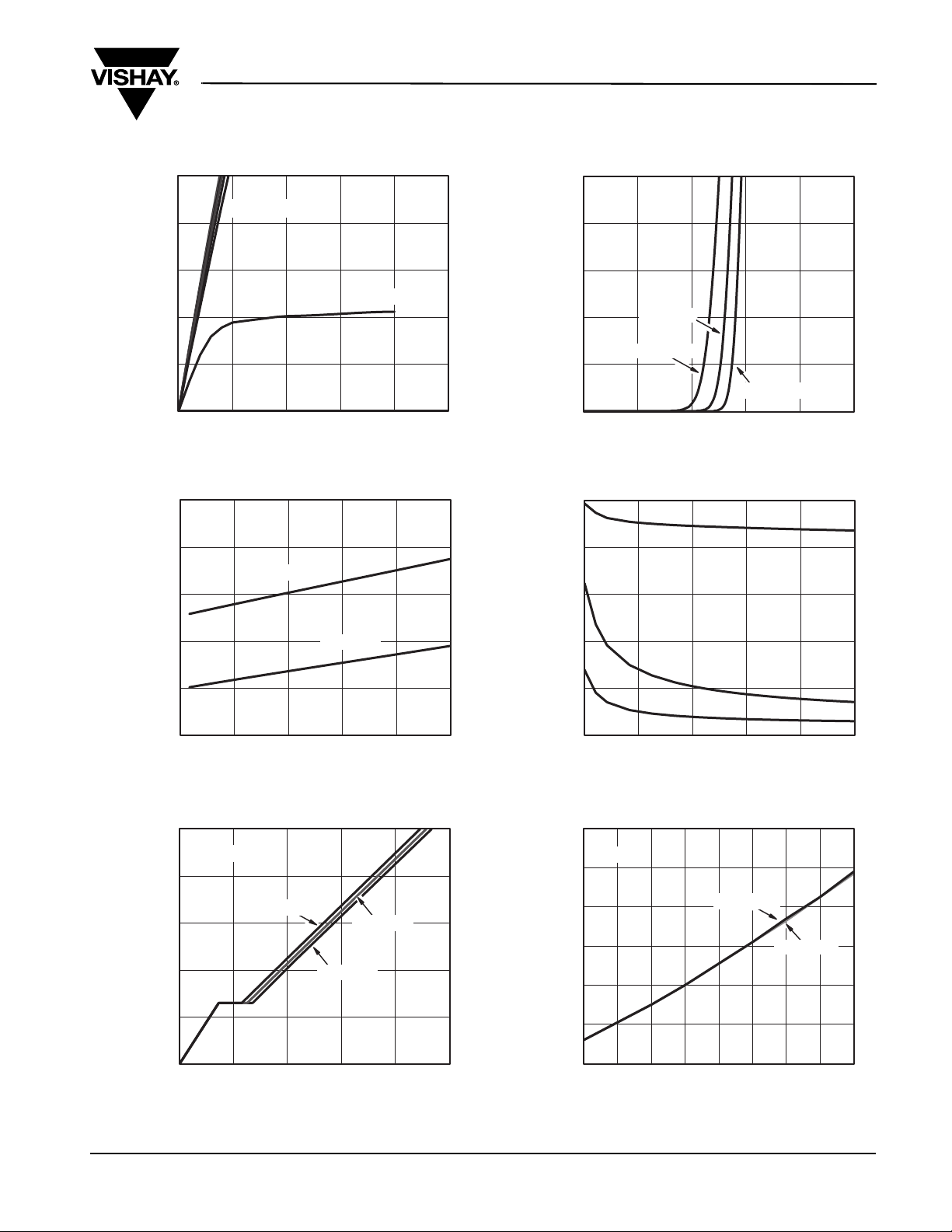
TYPICAL CHARACTERISTICS 25 °C, unless otherwise noted
Si4932DY
Vishay Siliconix
30
24
18
12
- Drain Current (A)I
D
6
0
0.0 0.5 1.0 1.5 2.0 2.5
VGS=10thru 4 V
V
- Drain-to-Source Voltage (V)
DS
Output Characteristics
0.016
0.015
VGS=4.5V
0.014
VGS=3V
5
4
3
2
- Drain Current (A)I
D
1
0
012345
TC= 25 °C
TC= 125 °C
TC=- 55 °C
VGS- Gate-to-Source Voltage (V)
Transfer Characteristics
2000
1600
1200
C
iss
0.013
- On-Resistance (Ω)R
DS(on)
0.012
0.011
0 6 12 18 24 30
ID- Drain Current (A)
VGS=10V
On-Resistance vs. Drain Current
10
ID=5A
8
6
4
- Gate-to-Source Voltage (V)
GS
2
V
0
0 7 14 21 28 35
VDS=10V
VDS=15V
VDS=20V
Qg- Total Gate Charge (nC)
Gate Charge
800
C - Capacitance (pF)
400
C
rss
0
0.0 2.4 4.8 7.2 9.6 12
C
oss
VDS- Drain-to-Source Voltage (V)
Capacitance
1.8
ID=7A
1.6
1.4
1.2
- On-Resistance
(Normalized)
1.0
DS(on)
R
0.8
0.6
- 50 - 25 0 25 50 75 100 125 150
-Junction Temperature (°C)
T
J
VGS=10V
On-Resistance vs. Junction Temperature
VGS=4.5V
Document Number: 69012
S-83042-Rev. A, 22-Dec-08
www.vishay.com
3
 Loading...