

Vishay Si4925BDY Datasheet
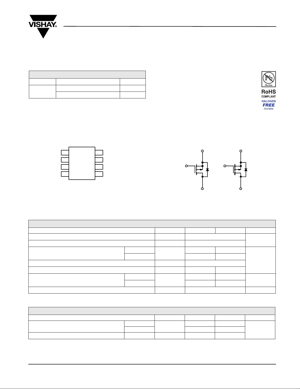
Dual P-Channel 30-V (D-S) MOSFET
Si4925BDY
Vishay Siliconix
PRODUCT SUMMARY
VDS (V) R
1
1
2
2
0.025 at V
0.041 at V
1
2
3
4
Top View
- 30
S
G
S
G
Ordering Information: Si4925BDY-T1-E3 (Lead (Pb)-free)
Si4925BDY-T1-GE3 (Lead (Pb)-free and Halogen-free)
(Ω)I
DS(on)
= - 10 V
GS
= - 4.5 V
GS
SO-8
D
8
1
D
7
1
D
6
2
D
5
2
(A)
D
- 7.1
- 5.5
FEATURES
• Halogen-free According to IEC 61249-2-21
Definition
• TrenchFET
®
Power MOSFET
• Compliant to RoHS Directive 2002/95/EC
APPLICATIONS
• Load Switches
- Notebook PCs
- Desktop PCs
- Game Stations
G
1
P-Channel MOSFET
S
1
G
2
D
1
P-Channel MOSFET
S
2
D
2
ABSOLUTE MAXIMUM RATINGS TA = 25 °C, unless otherwise noted
Parameter Symbol 10 s Steady State Unit
Drain-Source Voltage
Gate-Source Voltage
Continuous Drain Current (T
= 150 °C)
J
a
Pulsed Drain Current
Continuous Source Current (Diode Conduction)
Maximum Power Dissipation
a
a
Operating Junction and Storage Temperature Range
TA = 25 °C
= 70 °C
T
A
TA = 25 °C
= 70 °C
T
A
V
DS
V
GS
I
D
I
DM
I
S
P
D
T
, T
J
stg
- 7.1 - 5.3
- 5.7 - 4.3
- 1.7 - 0.9
- 30
± 20
- 40
2.0 1.1
1.3 0.7
- 55 to 150 °C
V
A
W
THERMAL RESISTANCE RATINGS
Parameter Symbol Typical Maximum Unit
Maximum Junction-to-Ambient
a
t ≤ 10 s
Steady State 85 110
Maximum Junction-to-Foot (Drain) Steady State
Notes:
a. Surface Mounted on 1" x 1" FR4 board.
R
thJA
R
thJF
50 62.5
°C/W
30 40
Document Number: 72001
S09-0869-Rev. D, 18-May-09
www.vishay.com
1
Si4925BDY
Vishay Siliconix
SPECIFICATIONS TJ = 25 °C, unless otherwise noted
Parameter Symbol Test Conditions Min. Typ. Max. Unit
Static
V
Gate Threshold Voltage
Gate-Body Leakage
Zero Gate Voltage Drain Current
On-State Drain Current
a
Drain-Source On-State Resistance
Forward Transconductance
Diode Forward Voltage
Dynamic
b
a
a
Total Gate Charge
Gate-Drain Charge
Tur n - O n D e l ay Time
Rise Time
Turn-Off Delay Time
Fall Ti me
Source-Drain Reverse Recovery Time
V
GS(th)
I
GSS
I
DSS
I
D(on)
a
R
DS(on)
g
fs
V
SD
Q
g
Q
gs
Q
gd
t
d(on)
t
r
t
d(off)
t
f
t
rr
V
V
VDS = - 15 V, V
I
D
Notes:
a. Pulse test; pulse width ≤ 300 µs, duty cycle ≤ 2 %.
b. Guaranteed by design, not subject to production testing.
Stresses beyond those listed under “Absolute Maximum Ratings” may cause permanent damage to the device. These are stress ratings only, and functional operation
of the device at these or any other conditions beyond those indicated in the operational sections of the specifications is not implied. Exposure to absolute maximum
rating conditions for extended periods may affect device reliability.
= VGS, ID = - 250 µA
DS
VDS = 0 V, VGS = ± 20 V
V
= - 30 V, V
DS
= - 30 V, V
DS
= - 5 V, V
DS
V
= - 10 V, ID = - 7.1 A
GS
V
= - 4.5 V, ID = - 5.5 A
GS
GS
= 0 V
GS
= 0 V, TJ = 55 °C
= - 10 V
GS
VDS = - 10 V, ID = - 7.1 A
IS = - 1.7 A, V
GS
V
= - 15 V, RL = 15 Ω
DD
≅ - 1 A, V
GEN
= 0 V
GS
= - 10 V, ID = - 7.1 A
= - 10 V, Rg = 6 Ω
IF = - 1.7 A, dI/dt = 100 A/µs
- 1 - 3 V
± 100 nA
- 1
- 25
- 40 A
0.020 0.025
0.033 0.041
20 S
- 0.8 - 1.2 V
33 50
5.4
8.9
915
12 20
60 90
34 50
30 60
µA
Ω
nCGate-Source Charge
ns
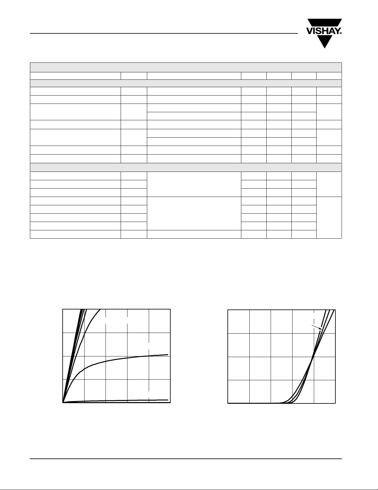
TYPICAL CHARACTERISTICS 25 °C, unless otherwise noted
40
VGS = 10 V thru 5 V
30
4V
20
- Drain Current (A)I
D
10
3 V, 2 V
0
012345
- Drain-to-Source Voltage (V)
V
DS
Output Characteristics
www.vishay.com
2
40
TC = - 55 °C
25 °C
30
20
- Drain Current (A)
D
I
10
0
012345
VGS - Gate-to-Source Voltage (V)
Transfer Characteristics
Document Number: 72001
S09-0869-Rev. D, 18-May-09
125 °C
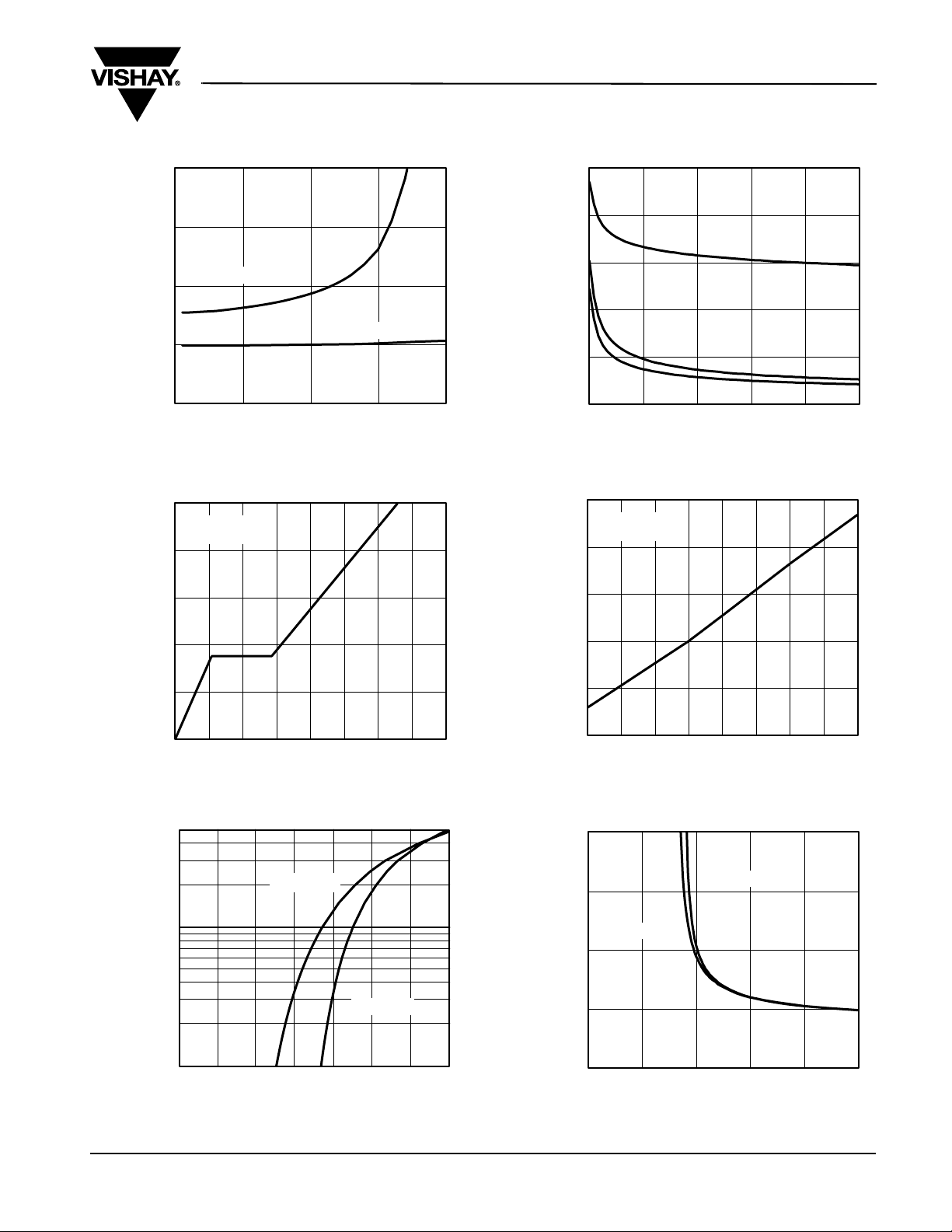
TYPICAL CHARACTERISTICS 25 °C, unless otherwise noted
0.08
Si4925BDY
Vishay Siliconix
2500
0.06
0.04
VGS = 4.5 V
- On-Resistance (Ω)
DS(on)
0.02
R
0.00
0 10203040
On-Resistance vs. Drain Current
10
VDS = 15 V
I
= 7.1 A
D
8
6
4
- Gate-to-Source Voltage (V)
2
GS
V
I
- Drain Current (A)
D
VGS = 10 V
2000
1500
1000
C - Capacitance (pF)
500
C
rss
0
0 6 12 18 24 30
1.6
VGS = 10 V
I
= 7.1 A
1.4
1.2
- On-Resistance
1.0
DS(on)
R
Normalized
0.8
D
C
iss
C
oss
VDS - Drain-to-Source Voltage (V)
Capacitance
0
0 5 10 15 20 25 30 35 40
50
10
- Source Current (A)
S
I
1
0.0 0.2 0.4 0.6 0.8 1.0 1.2 1.4
V
SD
Source-Drain Diode Forward Voltage
Document Number: 72001
S09-0869-Rev. D, 18-May-09
Qg - Total Gate Charge (nC)
Gate Charge
TJ = 150 °C
TJ = 25 °C
- Source-to-Drain Voltage (V)
0.6
- 50 - 25 0 25 50 75 100 125 150
T
- Junction Temperature (°C)
J
On-Resistance vs. Junction Temperature
0.08
0.06
ID = 3 A
0.04
ID = 7.1 A
- On-Resistance (Ω)
DS(on)
0.02
R
0.00
0246810
VGS - Gate-to-Source Voltage (V)
On-Resistance vs. Gate-to-Source Voltage
www.vishay.com
3
 Loading...