

Vishay si4914bd Datasheet
Si4914BDY
e
Vishay Siliconix
Dual N-Channel 30-V (D-S) MOSFET with Schottky Diode
PRODUCT SUMMARY
Channel-1
Channel-2
VDS (V) R
0.021 at V
0.027 at V
30
0.020 at V
0.025 at V
DS(on)
(Ω)
GS
GS
GS
GS
= 10 V
= 4.5 V
= 10 V
= 4.5 V
I
(A)
D
8.4
7.4
d
8
d
8
SCHOTTKY PRODUCT SUMMARY
(V)
V
VDS (V)
Diode Forward Voltage
SD
a
Qg (Typ.)
I
F
6.7
7.0
(A)
FEATURES
• Halogen-free According to IEC 61249-2-21
Definition
• LITTLE FOOT
• 100 % R
®
Plus Integrated Schottky
and UIS Tested
g
• Compliant to RoHS Directive 2002/95/EC
APPLICATIONS
• Notebook PC
- System Power dc-to-dc
D
1
30 0.50 V at 1.0 A 2.0
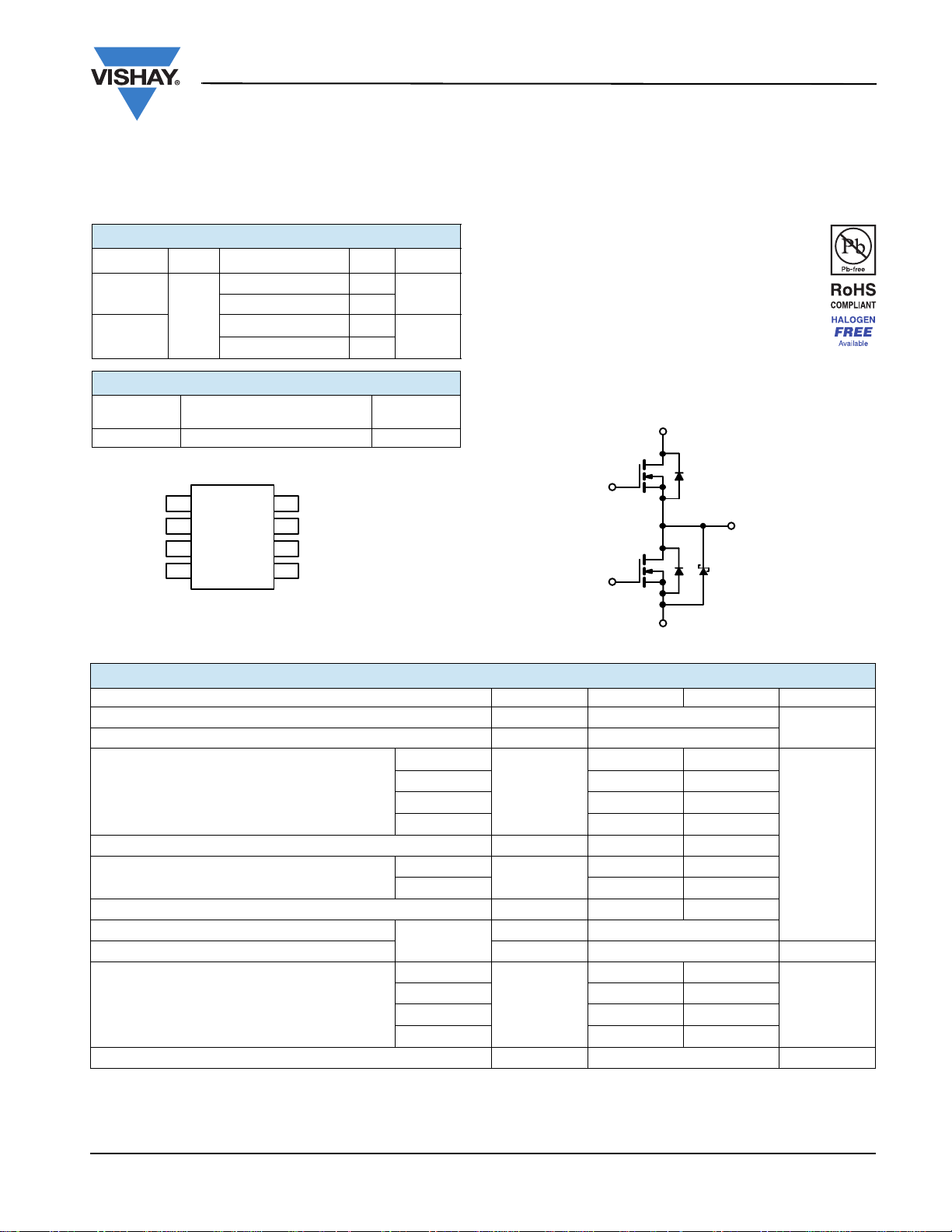
SO-8
D
1
1
D
2
1
G
3
2
S
4
2
T op V i e w
Ordering Information: Si4914BDY-T1-E3 (Lead (Pb)-free)
Si4914BDY-T1-GE3 (Lead (Pb)-free and Halogen-free)
G
8
1
S 1 /D
7
6
5
S 1 /D
S 1 /D
2
2
2
G
1
N-Channel 1
MOSFET
G
2
N-Channel 2
MOSFET
S1/D
2
Schottky Diod
S
2
ABSOLUTE MAXIMUM RATINGS TA = 25 °C, unless otherwise noted
Parameter Symbol Channel-1 Channel-2 Unit
Drain-Source Voltage
Gate-Source Voltage
Continuous Drain Current (T
= 150 °C)
J
a, b
Pulsed Drain Current (10 µs Pulse Width)
Continuous Source-Drain Diode Current
PulseD Source-Drain Current
Single-Pulse Avalanche Current
Single-Pulse Avalanche Energy
Maximum Power Dissipation
a, b
Operating Junction and Storage Temperature Range
Notes:
a. Based on T
b. Surface Mounted on 1" x 1" FR4 board.
= 25 °C.
C
c. t = 10 s.
d. Package limited.
Document Number: 69654
S09-2109-Rev. E, 12-Oct-09
TC = 25 °C
T
= 70 °C
C
T
= 25 °C
A
TA = 70 °C
T
= 25 °C
C
= 25 °C
T
A
L = 0.1 mH
TC = 25 °C
T
= 70 °C
C
T
= 25 °C
A
TA = 70 °C
V
DS
V
GS
8.4
I
D
6.7 7.4
6.7
5.3
I
DM
I
S
I
SM
I
AS
E
AS
40 40
2.4 2.8
1.0
40 40
2.7 3.1
P
D
1.7 2.0
1.7
1.1
, T
T
J
stg
30
20
d
8
b, c
b, c
b, c
7.4
5.7
1.1
b, c
b, c
b, c
15
11.2 mJ
b, c
b, c
2.0
1.2
b, c
b, c
- 55 to 150 °C
www.vishay.com
V
A
W
1
Si4914BDY
Vishay Siliconix
THERMAL RESISTANCE RATINGS
Channel-1 Channel-2
Parameter
Maximum Junction-to-Ambient
a
t ≤ 10 s
Maximum Junction-to-Foot (Drain) Steady State
Notes:
a. Surface Mounted on 1" x 1" FR4 board.
b. Maximum under Steady State conditions is 120 °C/W for Channel 1 and 115 °C/W for Channel 2.
MOSFET SPECIFICATIONS TJ = 25 °C, unless otherwise noted
Parameter Symbol Test Conditions Min. Typ.
Static
Drain-Source Breakdown Voltage
Temperature Coefficient ΔVDS/T
V
DS
V
Temperature Coefficient ΔV
GS(th)
Gate Threshold Voltage
Gate-Body Leakage
Zero Gate Voltage Drain Current
On-State Drain Current
b
Drain-Source On-State Resistance
Forward Transconductance
Diode Forward Voltage
Dynamic
a
b
b
Total Gate Charge
Gate-Source Charge
Gate-Drain Charge
Gate Resistance
V
DS
J
GS(th)/TJ
V
GS(th)
I
GSS
I
DSS
V
I
V
D(on)
b
R
DS(on)
g
fs
V
SD
Q
g
V
Q
gs
V
Q
gd
R
g
Symbol
R
thJA
R
thJF
VGS = 0 V, ID = 250 µA
ID = 250 µA
V
= VGS, ID = 250 µA
DS
VDS = 0 V, VGS = 20 V
V
= 30 V, V
DS
= 30 V, V
DS
DS
V
V
V
GS
V
GS
= 0 V, TJ = 85 °C
GS
= 5 V, V
GS
= 10 V, ID = 8 A
GS
= 10 V, ID = 8 A
GS
= 4.5 V, ID = 6 A
= 4.5 V, ID = 6 A
VDS = 15 V, ID = 8 A
V
= 15 V, ID = 8 A
DS
IS = 1.7 A, V
I
= 1 A, V
S
GS
GS
Channel-1
= 15 V, V
DS
= 4.5 V, ID = 8 A
GS
Channel-2
= 15 V, V
DS
= 4.5 V, ID = 8 A
GS
59 70 52 62.5
36 45 32 40
Ch-1 30
Ch-2 30
Ch-1 35 mV/°C
Ch-1 - 6.2
Ch-1 1.2 2.7
Ch-2 1.2 2.7
Ch-1 100
Ch-2 100
GS
= 0 V
Ch-1 1
Ch-2 100
Ch-1 15
Ch-2 10000
= 10 V
Ch-1 20
Ch-2 20
Ch-1 0.0165 0.021
Ch-2 0.0155 0.020
Ch-1 0.0215 0.027
Ch-2 0.020 0.025
Ch-1 29
Ch-2 33
= 0 V
= 0 V
Ch-1 0.77 1.1
Ch-2 0.46 0.5
Ch-1 6.7 10.5
Ch-2 7.0 11.0
Ch-1 2.8
Ch-2 2.8
Ch-1 2.0
Ch-2 2.0
Ch-1 2.9 6.0
Ch-2 2.0 4.0
a
Max. Unit
Unit Typ. Max. Typ. Max.
°C/W
V
V
nA
µA
A
Ω
S
V
nC
Ω
www.vishay.com
2
Document Number: 69654
S09-2109-Rev. E, 12-Oct-09
MOSFET SPECIFICATIONS TJ = 25 °C, unless otherwise noted
Parameter Symbol Test Conditions Min. Typ.
Dynamic
Tu r n - O n D el a y T i m e
Rise Time
Turn-Off Delay Time
Fall Time
Source-Drain Reverse Recovery Time
Body Diode Reverse Recovery Charge
Reverse Recovery Fall Time
Reverse Recovery Rise Time
Notes:
a. Guaranteed by design, not subject to production testing.
b. Pulse test; pulse width ≤ 300 µs, duty cycle ≤ 2 %.
a
t
d(on)
t
d(off)
Q
t
r
≅ 5 A, V
I
D
I
≅ 5 A, V
t
f
t
rr
D
Channel-1
V
= 15 V, RL = 3 Ω
DD
= 10 V, Rg = 1 Ω
GEN
Channel-2
V
= 15 V, RL = 3 Ω
DD
= 10 V, Rg = 1 Ω
GEN
IF = 2.2 A, dI/dt = 100 A/µs
I
= 2.2 A, dI/dt = 100 A/µs
F
IF = 2.2 A, dI/dt = 100 A/µs
rr
t
a
t
b
I
= 2.2 A, dI/dt = 100 A/µs
F
IF = 2.2 A, dI/dt = 100 A/µs
I
= 2.2 A, dI/dt = 100 A/µs
F
IF = 2.2 A, dI/dt = 100 A/µs
I
= 2.2 A, dI/dt = 100 A/µs
F
Ch-1 9 18
Ch-2 10 20
Ch-1 10 20
Ch-2 9 18
Ch-1 16 32
Ch-2 16 32
Ch-1 9 18
Ch-2 8 16
Ch-1 35 55
Ch-2 21 35
Ch-1 40
Ch-2 11
Ch-1 19
Ch-2 11
Ch-1 16
Ch-2 10
Si4914BDY
Vishay Siliconix
a
Max. Unit
ns
nC
ns
Stresses beyond those listed under “Absolute Maximum Ratings” may cause permanent damage to the device. These are stress ratings only, and fun ctional operation
of the device at these or any other conditions beyond those indicated in the operational sections of the specifications is not implied. Exposure to absolute maximum
rating conditions for extended periods may affect device reliability.
Document Number: 69654
S09-2109-Rev. E, 12-Oct-09
www.vishay.com
3
Si4914BDY
Vishay Siliconix
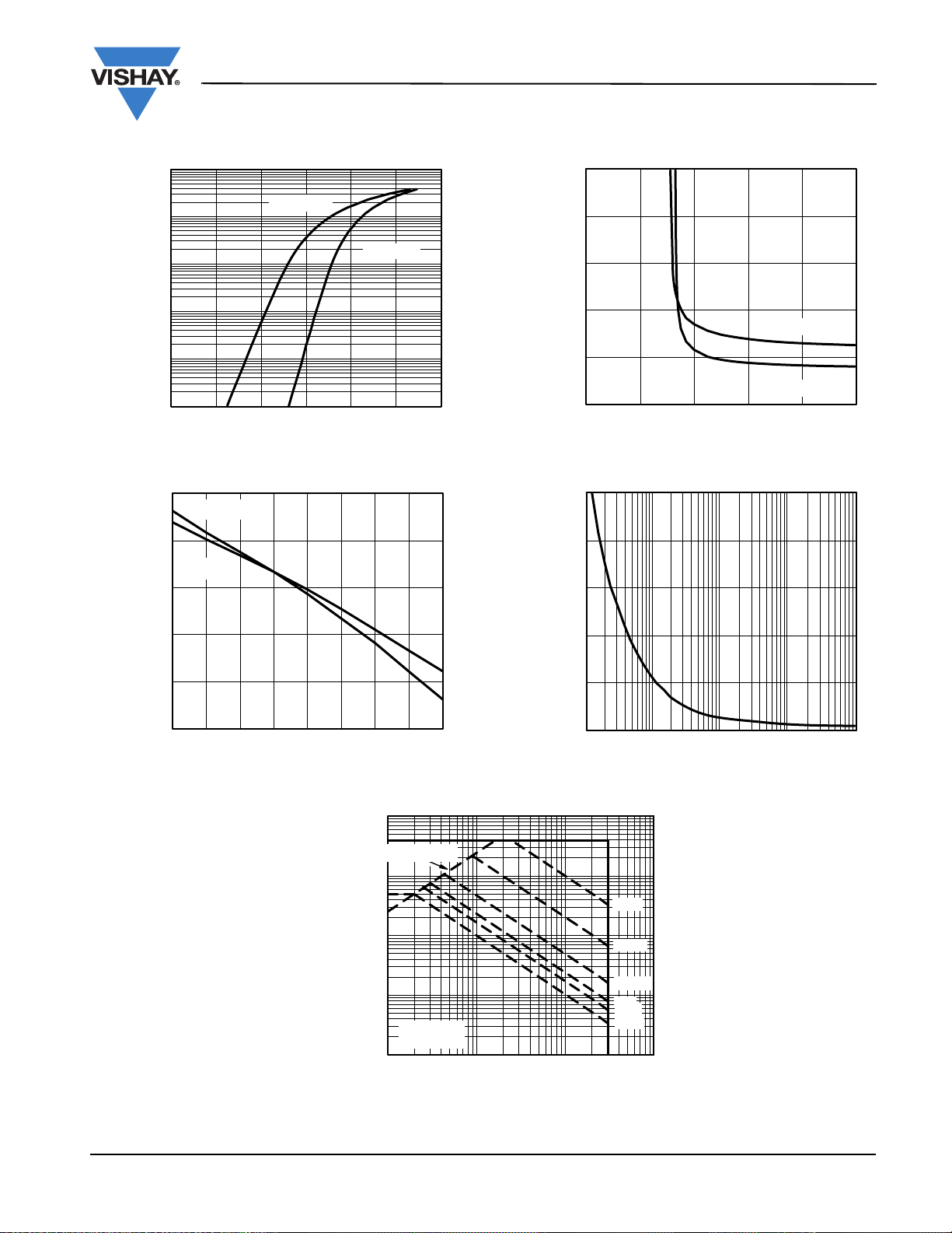
CHANNEL-1 TYPICAL CHARACTERISTICS 25 °C, unless otherwise noted
50
40
30
20
- Drain Current (A)I
D
10
0
00.51.01.52.02.5
VDS- Drain-to-Source Voltage (V)
VGS=10V thru 5 V
4 V
3 V
Output Characteristics
0.05
0.04
0.03
VGS=4.5V
2.0
1.6
1.2
TC= 25 °C
0.8
- Drain Current (A)I
D
0.4
0
TC= 125 °C
TJ= - 55 °C
012345
VGS- Gate-to-Source Voltage (V)
Transfer Characteristics
1000
C
800
600
iss
0.02
- On-Resistance (Ω)R
DS(on)
0.01
0
0 1020304050
ID- Drain Current (A)
VGS=10V
On-Resistance vs. Drain Current
10
ID= 8 A
8
6
4
- Gate-to-Source Voltage (V)
GS
2
V
0
0 3.2 6.4 9.6 12.8 16.0
VDS=15V
Qg- Total Gate Charge (nC)
VDS=10V
VDS=20V
Gate Charge
400
C - Capacitance (pF)
200
C
rss
0
0 6 12 18 24 30
1.7
ID=7A
1.5
1.3
- On-Resistance
1.1
(Normalized)
DS(on)
R
0.9
0.7
- 50 - 25 0 25 50 75 100 125 150
On-Resistance vs. Junction Temperature
C
oss
VDS- Drain-to-Source Voltage (V)
Capacitance
VGS=10V
VGS=4.5V
TJ- Junction Temperature (°C)
www.vishay.com
4
Document Number: 69654
S09-2109-Rev. E, 12-Oct-09
CHANNEL-1 TYPICAL CHARACTERISTICS 25 °C, unless otherwise noted
100
0.10
Si4914BDY
Vishay Siliconix
10
1
0.1
- Source Current (A)I
S
0.01
0.001
0 0.2 0.4 0.6 0.8 1.0 1.2
VSD- Source-to-Drain Voltage (V)
TJ= 150 °C
TJ= 25 °C
Source-Drain Diode Forward Voltage
0.5
ID= 250 µA
0.2
ID=5mA
- 0.1
Variance (V)V
- 0.4
GS(th)
- On-Resistance (Ω)R
DS(on)
Power (W)
0.08
0.06
0.04
TA= 125 °C
0.02
TA= 25 °C
0
02468 10
VGS- Gate-to-Source Voltage (V)
On-Resistance vs. Gate-to-Source Voltage
100
80
60
40
- 0.7
- 1.0
- 50 - 25 0 25 50 75 100 125 150
TJ- Temperature (°C)
Threshold Voltage
100
Limited byR
10
1
- Drain Current (A)
D
I
0.1
Single Pulse
0.01
0.1 1 10 100
* V
*
DS(on)
TA=25 °C
VDS- Drain-to-Source Voltage (V)
> minimum VGSat which R
GS
Safe Operating Area
20
0
0.1
Time (s)
Single Pulse Power, Junction-to-Ambient
1ms
10 ms
100 ms
1s
10 s
DC
is specified
DS(on)
011100.00.01
Document Number: 69654
S09-2109-Rev. E, 12-Oct-09
www.vishay.com
5
 Loading...