

Vishay Si4856ADY Datasheet
Si4856ADY
30
21
V
b
C/W
PRODUCT SUMMARY
V
DS
(V)
0.0052 @ VGS = 10 V 17
0.0076 @ VGS = 4.5 V 14
Ordering Information: Si4856ADY—E3
r
(W)
DS(on)
SD
S
SD
G
New Product
N-Channel 30-V (D-S) MOSFET
FEATURES
D TrenchFETr Power MOSFETS
D 100% R
I
(A) Qg (Typ)
D
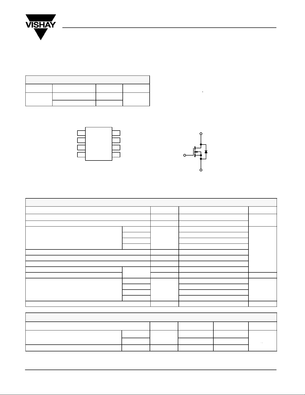
SO-8
1
2
3
4
Top View
Si4856ADY-T1—E3 (with Tape and Reel)
8
D
7
6
D
5
APPLICATIONS
D Buck Converter
D Synchronous Rectifier
G
Vishay Siliconix
Tested
g
− Secondary Rectifier
D
S
N-Channel MOSFET
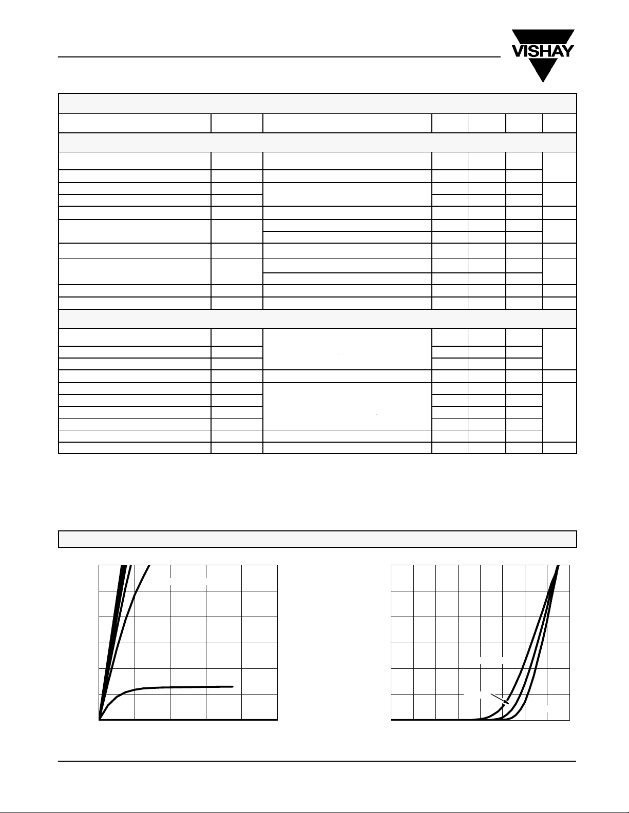
ABSOLUTE MAXIMUM RATINGS (TA = 25_C UNLESS OTHERWISE NOTED)
Parameter Symbol Limit Unit
Drain-Source Voltage V
Gate-Source Voltage V
TC = 25_C
a,
Continuous Drain Current (TJ = 150_C)
Pulsed Drain Current I
Continuous Source Current (Diode Conduction)
Pulse Source-Drain Diode Current I
Single Pulse Avalanche Current
Single Pulse Avalanche Energy
Maximum Power Dissipation
Operating Junction and Storage Temperature Range TJ, T
_
a, b
a
TC = 70_C
TA = 25_C
TA = 70_C
L = 0.1 mH
TC = 25_C
TC = 70_C
TA = 25_C
TA = 70_C
I
E
P
I
DM
I
SM
AS
DS
GS
D
S
AS
D
stg
30
"20
26
21
17
14
"50
2.7
50
45
100 mJ
6.5
4.2
3.0
2.0
−55 to 150
THERMAL RESISTANCE RATINGS
Parameter Symbol Typical Maximum Unit
Maximum Junction-to-Ambient (MOSFET)
Maximum Junction-to-Foot (Drain) Steady State R
Notes
a. Surface Mounted on 1” x 1” FR4 Board.
b. t = 10 sec
a
t v 10 sec
Steady State
R
thJA
thJF
34 41
67 80
15 19
A
W
_C
_C/W
Document Number: 73239
S-50031—Rev. A, 17-Jan-05
www.vishay.com
1
Si4856ADY
V
Drain-Source On-State Resistance
a
r
W
DS GS D
VDD = 15 V, RL = 15 W
g
Vishay Siliconix
New Product
MOSFET SPECIFICATIONS (TJ = 25_C UNLESS OTHERWISE NOTED)
Parameter Symbol Test Condition Min Typ Max Unit
Static
Gate Threshold Voltage V
Drain-Source Breakdown Voltage V
VDS Temperature Coefficient
V
Temperature Coefficient
GS(th)
Gate-Body Leakage I
Zero Gate Voltage Drain Current I
On-State Drain Current
-
Forward Transconductance
Diode Forward Voltage
Dynamic
b
a
-
a
a
a
Total Gate Charge Q
Gate-Source Charge Q
Gate-Drain Charge Q
Gate-Resistance R
Turn-On Delay Time t
Rise Time t
Turn-Off Delay Time t
Fall Time t
Source-Drain Reverse Recovery Time t
Body Diode Reverse Recovery Charge Q
Notes
a. Pulse test; pulse width v
b. Guaranteed by design, not subject to production testing.
300 ms, duty cycle v 2%.
DV
DV
GS(th)
DS
DS/Tj
GS(th)/Tj
GSS
DSS
I
D(on)
DS(on)
g
fs
V
SD
g
gs
gd
g
d(on)
r
d(off)
f
rr
rr
VDS = VGS, I
VGS = 0 V, I
I
= 250 mA
D
= 250 mA
D
= 250 mA
D
VDS = 0 V, VGS = "20 V
VDS = 30 V, VGS = 0 V 1
VDS = 30 V, VGS = 0 V, TJ = 70_C
VDS w 5 V, VGS = 10 V
VGS = 10 V, ID = 17 A
VGS = 4.5 V, ID = 14 A 0.0063 0.0076
VDS = 15 V, ID = 17 A 57 S
IS = 2.7 A, VGS = 0 V 0.72 1.1 V
V
= 15 V, VGS = 4.5 V, ID = 17 A 8.2 nC
DS
VDD = 15 V, RL = 15 W
ID ^ 1 A, V
= 10 V, Rg = 6 W
GEN
IF = 2.7 A, di/dt = 100 A/ms
IF = 2.9 A, di/dt = 100 A/ms
Stresses beyond those listed under “Absolute Maximum Ratings” may cause permanent damage to the device. These are stress ratings only , and functional operation
of the device at these or any other conditions beyond those indicated in the operational sections of the specifications is not implied. Exposure to absolute maximum
rating conditions for extended periods may affect device reliability .
1.5 2.5
30
24
−6.2
mV/_C
"100 nA
5
40 A
0.0043 0.0052
21 32
7.2
0.7 1.5 2.3
18 27
15 23
57 90
20 30
40 60
36 60 nC
_
mA
W
ns
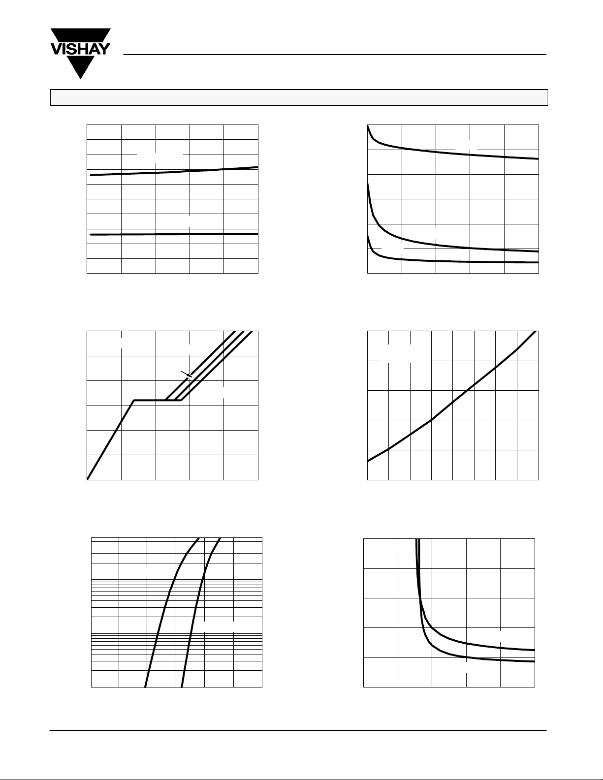
TYPICAL CHARACTERISTICS (25_C UNLESS NOTED)
60
50
40
30
20
− Drain Current (A)I
D
10
0
0.0 0.4 0.8 1.2 1.6 2.0
www.vishay.com
2
Output Characteristics Transfer Characteristics
VGS = 10 thru 4 V
VDS − Drain-to-Source Voltage (V)
3 V
60
50
40
30
20
− Drain Current (A)I
D
10
TC = 125_C
25_C
0
0.0 0.5 1.0 1.5 2.0 2.5 3.0 3.5 4.0
VGS − Gate-to-Source Voltage (V)
Document Number: 73239
S-50031—Rev. A, 17-Jan-05
−55_C
Si4856ADY
New Product
TYPICAL CHARACTERISTICS (25_C UNLESS NOTED)
0.0080
0.0075
0.0070
W )
0.0065
0.0060
0.0055
0.0050
− On-Resistance (r
0.0045
DS(on)
0.0040
0.0035
0.0030
− Gate-to-Source Voltage (V)
GS
V
6
5
4
3
2
1
On-Resistance vs. Drain Current
VGS = 4.5 V
VGS = 10 V
0 1020304050
ID − Drain Current (A)
Gate Charge
ID = 17 A
VDS = 10 V
15 V
20 V
3600
3000
2400
1800
1200
C − Capacitance (pF)
600
0
0 6 12 18 24 30
On-Resistance vs. Junction Temperature
1.6
1.4
1.2
1.0
− On-Resiistance
(Normalized)
DS(on)
r
0.8
Vishay Siliconix
Capacitance
C
oss
C
rss
V
− Drain-to-Source Voltage (V)
DS
VGS = 10 V
= 17 A
I
D
C
iss
0
0 6 12 18 24 30
Qg − Total Gate Charge (nC)
Source-Drain Diode Forward Voltage On-Resistance vs. Gate-to-Source Voltage
60
10
1
− Source Current (A)I
S
0.1
0.00 0.2 0.4 0.6 0.8
VSD − Source-to-Drain Voltage (V) VGS − Gate-to-Source Voltage (V)
Document Number: 73239
S-50031—Rev. A, 17-Jan-05
TJ = 150_C
TJ = 25_C
1.0 1.2
0.6
−50 −25 0 25 50 75 100 125 150
T
− Junction Temperature (_C)
J
0.025
0.020
W )
0.015
0.010
− On-Resistance (r
0.005
DS(on)
0.000
ID = 17 A
TJ = 125_C
TJ = 25_C
0246810
www.vishay.com
3
 Loading...