

Vishay Si4456DY Datasheet

N-Channel 40-V (D-S) MOSFET
Si4456DY
Vishay Siliconix
PRODUCT SUMMARY
VDS (V) R
40
0.0038 at V
0.0045 at V
(Ω)I
DS(on)
= 10 V 33
GS
= 4.5 V 31
GS
D
(A)
a
Qg (Typ.)
37.5 nC
FEATURES
• Halogen-free According to IEC 61249-2-21
Available
•TrenchFET
• 100 % R
®
Gen II Power MOSFET
and UIS Tested
g
APPLICATIONS
• Secondary Rectification
• Point of Load
SO-8
SD
1
SD
2
SD
3
GD
4
Top View
Ordering Information: Si4456DY-T1-E3 (Lead (Pb)-free)
Si4456DY-T1-GE3 (Lead (Pb)-free and Halogen-free)
8
7
6
5
G
N-Channel MOSFET
D
S
ABSOLUTE MAXIMUM RATINGS TA = 25 °C, unless otherwise noted
Parameter Symbol Limit Unit
Drain-Source Voltage
Gate-Source Voltage
Continuous Drain Current (T
Pulsed Drain Current
= 150 °C)
J
Continuous Source-Drain Diode Current
Avalanche Current
Single Pulse Avalanche Energy
Maximum Power Dissipation
Operating Junction and Storage Temperature Range
T
= 25 °C
C
= 70 °C 27
T
C
T
= 25 °C 23
A
TA = 70 °C 18
T
= 25 °C
C
T
= 25 °C 3.0
A
L = 0.1 mH
T
= 25 °C
C
T
= 70 °C 5.0
C
T
= 25 °C 3.5
A
TA = 70 °C 2.2
V
DS
V
GS
40
± 20
V
33
I
D
I
DM
I
S
I
AS
E
AS
70
7.0
40
80
b, c
b, c
A
b, c
mJ
7.8
P
D
, T
T
J
stg
b, c
b, c
- 55 to 150
W
THERMAL RESISTANCE RATINGS
Parameter Symbol Typical Maximum Unit
Maximum Junction-to-Ambient
Maximum Junction-to-Foot (Drain)
Notes:
a. Based on T
b. Surface Mounted on 1" x 1" FR4 board.
= 25 °C.
C
c. t = 5 s.
d. Maximum under steady state conditions is 80 °C/W.
Document Number: 73852
S09-0138-Rev. B, 02-Feb-09
b, d
t ≤ 5 s
Steady State
R
thJA
R
thJF
29 35
13 16
°C/W
www.vishay.com
1

Si4456DY
Vishay Siliconix
SPECIFICATIONS TJ = 25 °C, unless otherwise noted
Parameter Symbol Test Conditions Min. Typ. Max. Unit
Static
V
Drain-Source Breakdown Voltage
V
Temperature Coefficient ΔVDS/T
DS
Temperature Coefficient ΔV
V
GS(th)
Gate-Source Threshold Voltage
Gate-Source Leakage
Zero Gate Voltage Drain Current
On-State Drain Current
Drain-Source On-State Resistance
Forward Transconductance
Dynamic
b
a
a
a
Input Capacitance
Reverse Transfer Capacitance
Total Gate Charge
Gate-Source Charge
Gate-Drain Charge
Gate Resistance
Tur n - O n D e l ay Time
Rise Time
Turn-Off DelayTime
Fall Ti me
Tur n - O n D e l ay Time
Rise Time
Turn-Off DelayTime
Fall Ti me
V
DS
GS(th)/TJ
V
GS(th)
I
GSS
I
DSS
I
D(on)
R
DS(on)
g
fs
C
iss
C
oss
C
rss
Q
g
Q
gs
Q
gd
R
g
t
d(on)
t
r
t
d(off)
t
f
t
d(on)
t
r
t
d(off)
t
f
J
Drain-Source Body Diode Characteristics
Continous Source-Drain Diode Current
Pulse Diode Forward Current
a
Body Diode Voltage
Body Diode Reverse Recovery Time
Body Diode Reverse Recovery Charge
Reverse Recovery Fall Time
Reverse Recovery Rise Time
I
S
I
SM
V
SD
t
rr
Q
rr
t
a
t
b
Notes:
a. Pulse test; pulse width ≤ 300 µs, duty cycle ≤ 2 %.
b. Guaranteed by design, not subject to production testing.
V
DS
V
V
DS
V
DS
I
D
I
D
IF = 13 A, dI/dt = 100 A/µs, TJ = 25 °C
= 0 V, ID = 250 µA
GS
ID = 250 µA
V
= VGS, ID = 250 µA
DS
VDS = 0 V, VGS = ± 20 V
V
= 40 V, VGS = 0 V
DS
= 40 V, V
V
DS
V
V
GS
V
= 20 V, V
DS
= 20 V, V
= 20 V, V
GS
DS
= 0 V, TJ = 55 °C
GS
= ≥ 5 V, V
GS
= 10 V, ID = 20 A
= 4.5 V, ID = 15 A
= 15 V, ID = 20 A
= 0 V, f = 1 MHz
GS
= 10 V, ID = 20 A
GS
= 4.5 V, ID = 20 A
GS
f = 1 MHz 1.05 1.6 Ω
V
= 20 V, RL = 2 Ω
DD
≅ 10 A, V
V
≅ 10 A, V
= 4.5 V, Rg = 1 Ω
GEN
= 20 V, RL = 2 Ω
DD
= 10 V, Rg = 1 Ω
GEN
TC = 25 °C
IS = 3 A
40 V
54
- 7
mV/°C
1.5 2.8 V
± 100 nA
1
10
= 10 V 30 A
0.0031 0.0038
0.0037 0.0045
110 S
5670
621
287
81 122
37.5 57
17
nC
11
145 220
208 320
56 85
15 23
21 32
58 90
55 85
815
7
70
0.71 1.1 V
38 60 ns
42 65 nC
21
17
µA
Ω
pFOutput Capacitance
ns
A
ns
Stresses beyond those listed under “Absolute Maximum Ratings” may cause permanent damage to the de vice. These are stress rating s only, and functiona l operation
of the device at these or any other conditions beyond those indicated in the operational sections of the specifications is not implied. Exposure to absolute maximum
rating conditions for extended periods may affect device reliability.
www.vishay.com
2
Document Number: 73852
S09-0138-Rev. B, 02-Feb-09
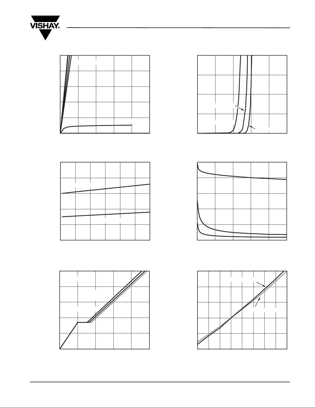
TYPICAL CHARACTERISTICS TA = 25 °C, unless otherwise noted
0.004
1.6
0
70
VGS = 10 V thru 4 V
56
)A( tnerruC niarD -I
42
28
D
14
0
0.0 0.5 1.0 1.5 2.0 2.5
- Drain-to-Source Voltage (V)
V
DS
VGS = 3 V
Output Characteristics
1.2
0.9
)A( tnerruC niarD -I
0.6
D
0.3
0.0
Si4456DY
Vishay Siliconix
TC = 25 °C
TC = 125 °C
TC = - 55 °C
012345
- Gate-to-Source Voltage (V)
V
GS
Transfer Characteristics
5
0.0041
mΩ( ecnatsiseR-nO
0.0037
0.0033
-)
)no(SD
R
0.0029
0.0025
VGS = 4.5 V
VGS = 10 V
0 102030405060
- Drain Current (A)
I
D
On-Resistance vs. Drain Current and Gate Voltage
10
8
6
4
2
ID = 20 A
VDS = 10 V
VDS = 20 V
VDS = 30 V
)V
(
e
ga
tl
oV
ec
ru
oS
-o
t-e
ta
G
-
SG
V
7000
C
iss
5600
)Fp( ec
4200
na
t
i
c
apaC
2800
-
C
1400
C
rss
0
0 8 16 24 32 40
C
oss
VDS - Drain-to-Source Voltage (V)
Capacitance
V
= 10 V, I D = 20 A
GS
1.4
ecn
at
)dezilam
si
1.2
seR-n
V
= 4.5 V, I D = 20 A
r
O -
oN(
1.0
)no(SD
R
0.8
GS
0
0 1734516885
Document Number: 73852
S09-0138-Rev. B, 02-Feb-09
Q g - Total Gate Charge (nC)
Gate Charge
0.6
- 50 - 25 0 25 50 75 100 125 15
TJ- Junction Temperature (°C)
On-Resistance vs. Junction Temperature
www.vishay.com
3
 Loading...