

Vishay Si4336DY Datasheet
Si4336DY
30
C/W
PRODUCT SUMMARY
V
DS
(V)
r
DS(on)
0.00325 @ VGS = 10 V 25
0.0042 @ VGS = 4.5 V 22
SD
1
SD
2
SD
3
GD
4
New Product
N-Channel 30-V (D-S) MOSFET
FEATURES
D Ultra Low On-Resistance Using High Density
TrenchFETr Gen II Power MOSFET Technology
D Q
Optimized
(W)
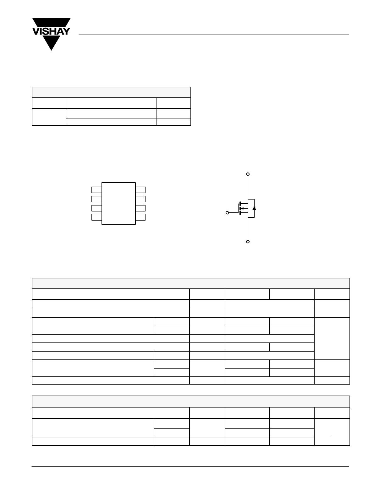
SO-8
I
(A)
D
8
7
6
5
g
D 100% R
Tested
g
APPLICATIONS
D Synchronous Buck Low-Side
− Notebook
− Server
− Workstation
D Synchronous Rectifier, POL
D
G
Vishay Siliconix
Top View
Ordering Information: Si4336DY
Si4336DY-T1 (with Tape and Reel)
S
N-Channel MOSFET
ABSOLUTE MAXIMUM RATINGS (TA = 25_C UNLESS OTHERWISE NOTED)
Parameter Symbol 10 secs Steady State Unit
Drain-Source Voltage V
Gate-Source Voltage V
a
Continuous Drain Current (TJ = 150_C)
Pulsed Drain Current (10 ms Pulse Width)
Continuous Source Current (Diode Conduction)
Avalanche Current L = 0.1 mH I
Maximum Power Dissipation
Operating Junction and Storage Temperature Range TJ, T
_
a
a
TA = 25_C
TA = 70_C
TA = 25_C
TA = 70_C
I
P
I
DM
I
AS
DS
GS
D
25 17
20 13
S
D
stg
2.9 1.3
3.5 1.6
2.2 1
30
"20
70
50
−55 to 150
THERMAL RESISTANCE RATINGS
V
A
W
_C
Maximum Junction-to-Ambient
Maximum Junction-to-Foot (Drain) Steady State R
Notes
a. Surface Mounted on 1” x 1” FR4 Board.
Document Number: 72417
S-31858—Rev. A, 15-Sep-03
Parameter Symbol Typical Maximum Unit
a
t v 10 sec
Steady State
R
thJA
thJF
29 35
67 80
13 16
www.vishay.com
_C/W
1
Si4336DY
Drain-Source On-State Resistance
a
r
W
VDD = 15 V, RL = 15 W
Vishay Siliconix
New Product
SPECIFICATIONS (TJ = 25_C UNLESS OTHERWISE NOTED)
Parameter Symbol Test Condition Min Typ Max Unit
Static
Gate Threshold Voltage V
Gate-Body Leakage I
Zero Gate Voltage Drain Current I
On-State Drain Current
-
Forward Transconductance
Diode Forward Voltage
Dynamic
b
a
-
a
a
a
Input Capacitance C
Output Capacitance C
Reverse Transfer Capacitance C
Total Gate Charge Q
Gate-Source Charge Q
Gate-Drain Charge Q
Gate Resistance R
Turn-On Delay Time t
Rise Time t
Turn-Off Delay Time t
Fall Time t
Source-Drain Reverse Recovery Time t
Notes
a. Pulse test; pulse width v
b. Guaranteed by design, not subject to production testing.
300 ms, duty cycle v 2%.
GS(th)
GSS
DSS
I
D(on)
DS(on)
g
fs
V
SD
iss
oss
rss
g
gs
gd
G
d(on)
r
d(off)
f
rr
VDS = VGS, I
= 250 mA
D
VDS = 0 V, VGS = "20 V
VDS = 30 V, VGS = 0 V 1
VDS = 30 V, VGS = 0 V, TJ = 55_C
VDS w 5 V, VGS = 10 V
VGS = 10 V, ID = 25 A
VGS = 4.5 V, ID = 22 A 0.0033 0.0042
VDS = 15 V, ID = 25 A 110 S
IS = 2.9 A, VGS = 0 V 0.72 1.1 V
V
= 15 V, VGS = 0 V, f = 1 MHz
DS
V
= 15 V, VGS = 4.5 V, ID = 20 A
DS
VDD = 15 V, RL = 15 W
ID ^ 1 A, V
= 10 V, RG = 6 W
GEN
IF = 2.9 A, di/dt = 100 A/ms
1.0 3.0 V
"100 nA
5
30 A
0.0026 0.00325
5600
860
415
32 50
16.5
8.5
0.8 1.3 2.0
24 35
16 25
90 140
32 50
45 70
mA
pF
nC
W
ns
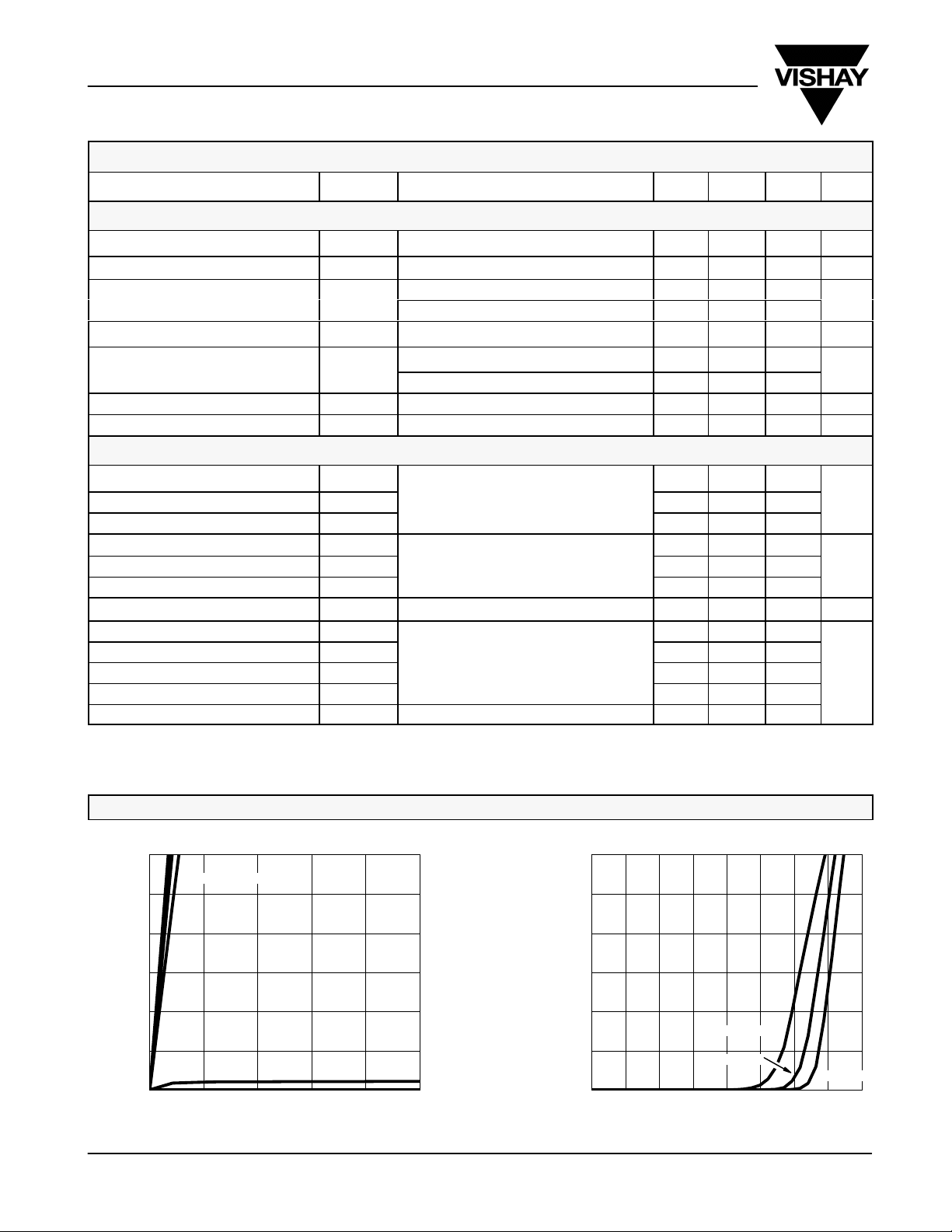
TYPICAL CHARACTERISTICS (25_C UNLESS NOTED)
60
50
40
30
20
− Drain Current (A)I
D
10
0
0.0 0.4 0.8 1.2 1.6 2.0
www.vishay.com
2
Output Characteristics Transfer Characteristics
VGS = 10 thru 4 V
VDS − Drain-to-Source Voltage (V)
3 V
60
50
40
30
20
− Drain Current (A)I
D
10
TC = 125_C
25_C
0
0.0 0.5 1.0 1.5 2.0 2.5 3.0 3.5 4.0
VGS − Gate-to-Source Voltage (V)
Document Number: 72417
S-31858—Rev. A, 15-Sep-03
−55_C
 Loading...