

Page 1
New Product
D
N-Channel 30-V (D-S) MOSFET
Si4174DY
Vishay Siliconix
PRODUCT SUMMARY
VDS (V) R
0.0095 at V
30
0.013 at V
DS(on)
(Ω)
GS
GS
= 10 V
= 4.5 V
I
D
(A)
17
14.5
a
Qg (Typ.)
8 nC
FEATURES
• Halogen-free According to IEC 61249-2-21
• TrenchFET
• 100 % R
®
Power MOSFET
and UIS Tested
g
APPLICATIONS
• Notebook CPU Core
- High-Side Switch
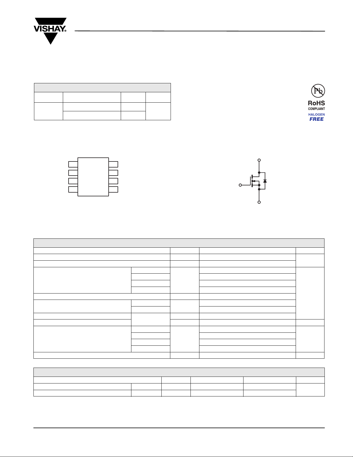
SO-8
SD
1
SD
2
SD
3
GD
4
Top View
Ordering Information: Si4174DY-T1-GE3 (Lead (Pb)-free and Halogen-free)
8
7
6
5
G
N-Channel MOSFET
S
ABSOLUTE MAXIMUM RATINGS TA = 25 °C, unless otherwise noted
Parameter Symbol Limit Unit
Drain-Source Voltage
Gate-Source Voltage
T
Continuous Drain Current (T
= 150 °C)
J
T
T
TA = 70 °C
Pulsed Drain Current
Continuous Source-Drain Diode Current
Single Pulse Avalanche Current
Avalanche Energy
T
T
L = 0.1 mH
T
Maximum Power Dissipation
T
T
TA = 70 °C
Operating Junction and Storage Temperature Range
= 25 °C
C
= 70 °C
C
= 25 °C
A
= 25 °C
C
= 25 °C
A
= 25 °C
C
= 70 °C
C
= 25 °C
A
V
DS
V
GS
30
± 20
V
17
I
D
I
DM
I
S
I
AS
E
AS
13.5
12
9.6
2.2
50
4.5
20
20
b, c
b, c
b, c
A
mJ
5
P
D
T
, T
J
stg
3.2
b, c
2.5
b, c
1.6
- 55 to 150
W
°C
THERMAL RESISTANCE RATINGS
Parameter Symbol Typical Maximum Unit
Maximum Junction-to-Ambient
Maximum Junction-to-Foot (Drain) Steady State
Notes:
a. Based on T
b. Surface Mounted on 1" x 1" FR4 board.
= 25 °C.
C
c. t = 10 s.
d. Maximum under Steady State conditions is 85 °C/W.
Document Number: 68998
S-82773-Rev. A, 17-Nov-08
b, d
t ≤ 10 s
R
thJA
R
thJF
38 50
20 25
°C/W
www.vishay.com
1
Page 2
New Product
Si4174DY
Vishay Siliconix
SPECIFICATIONS TJ = 25 °C, unless otherwise noted
Parameter Symbol Test Conditions Min. Typ. Max. Unit
Static
Drain-Source Breakdown Voltage
V
Temperature Coefficient ΔVDS/T
DS
V
Temperature Coefficient ΔV
GS(th)
Gate-Source Threshold Voltage
Gate-Source Leakage
Zero Gate Voltage Drain Current
On-State Drain Current
Drain-Source On-State Resistance
Forward Transconductance
Dynamic
b
a
a
a
Input Capacitance
Reverse Transfer Capacitance
Total Gate Charge
Gate-Source Charge
Gate-Drain Charge
Gate Resistance
Tur n - O n D e l ay Time
Rise Time
Turn-Off Delay Time
Fall Ti me
Tur n - O n D e l ay Time
Rise Time
Turn-Off Delay Time
Fall Ti me
V
DS
J
GS(th)/TJ
V
GS(th)
I
GSS
I
DSS
I
V
D(on)
R
DS(on)
g
fs
C
iss
C
oss
C
rss
Q
g
Q
gs
Q
gd
R
g
t
d(on)
t
r
t
d(off)
t
f
t
d(on)
t
r
t
d(off)
t
f
Drain-Source Body Diode Characteristics
Continuous Source-Drain Diode Current
Pulse Diode Forward Current
a
Body Diode Voltage
Body Diode Reverse Recovery Time
Body Diode Reverse Recovery Charge
Reverse Recovery Fall Time
Reverse Recovery Rise Time
I
S
I
SM
V
SD
t
rr
Q
rr
t
a
t
b
Notes:
a. Pulse test; pulse width ≤ 300 µs, duty cycle ≤ 2 %
b. Guaranteed by design, not subject to production testing.
V
= 0 V, ID = 250 µA
GS
ID = 250 µA
V
DS
V
DS
V
DS
V
DS
VDS = V
V
DS
V
DS
= 30 V, V
DS
V
V
V
= 15 V, V
= 15 V, V
= 15 V, V
, ID = 250 µA
GS
= 0 V, V
GS
= 30 V, V
≥ 5 V, V
= 10 V, ID = 10 A
GS
GS
= 15 V, ID = 10 A
DS
GS
= 0 V, TJ = 55 °C
GS
GS
= 4.5 V, ID = 7 A
= 0 V, f = 1 MHz
GS
= 10 V, ID = 10 A
GS
= 4.5 V, ID = 10 A
GS
= ± 20 V
= 0 V
= 10 V
f = 1 MHz 0.3 1.3 2.6 Ω
V
= 15 V, RL = 1.5 Ω
DD
≅ 10 A, V
I
D
V
≅ 10 A, V
I
D
DD
= 4.5 V, Rg = 1 Ω
GEN
= 15 V, RL = 1.5 Ω
= 10 V, Rg = 1 Ω
GEN
TC = 25 °C
IS = 3 A
IF = 10 A, dI/dt = 100 A/µs, TJ = 25 °C
30 V
34
- 4.7
mV/°C
1.0 2.2 V
± 100 nA
1
10
30 A
0.0078 0.0095
0.0108 0.0130
30 S
985
205
76
18 27
812
2.4
2.3
14 25
12 24
19 35
918
816
10 20
16 30
918
4.5
50
0.76 1.1 V
14 28 ns
510nC
8
6
µA
Ω
pFOutput Capacitance
nC
ns
A
ns
Stresses beyond those listed under “Absolute Maximum Ratings” may cause permanent damage to the de vice. These are stress rating s only, and functiona l operation
of the device at these or any other conditions beyond those indicated in the operational sections of the specifications is not implied. Exposure to absolute maximum
rating conditions for extended periods may affect device reliability.
www.vishay.com
2
Document Number: 68998
S-82773-Rev. A, 17-Nov-08
Page 3
New Product
TYPICAL CHARACTERISTICS 25 °C, unless otherwise noted
Si4174DY
Vishay Siliconix
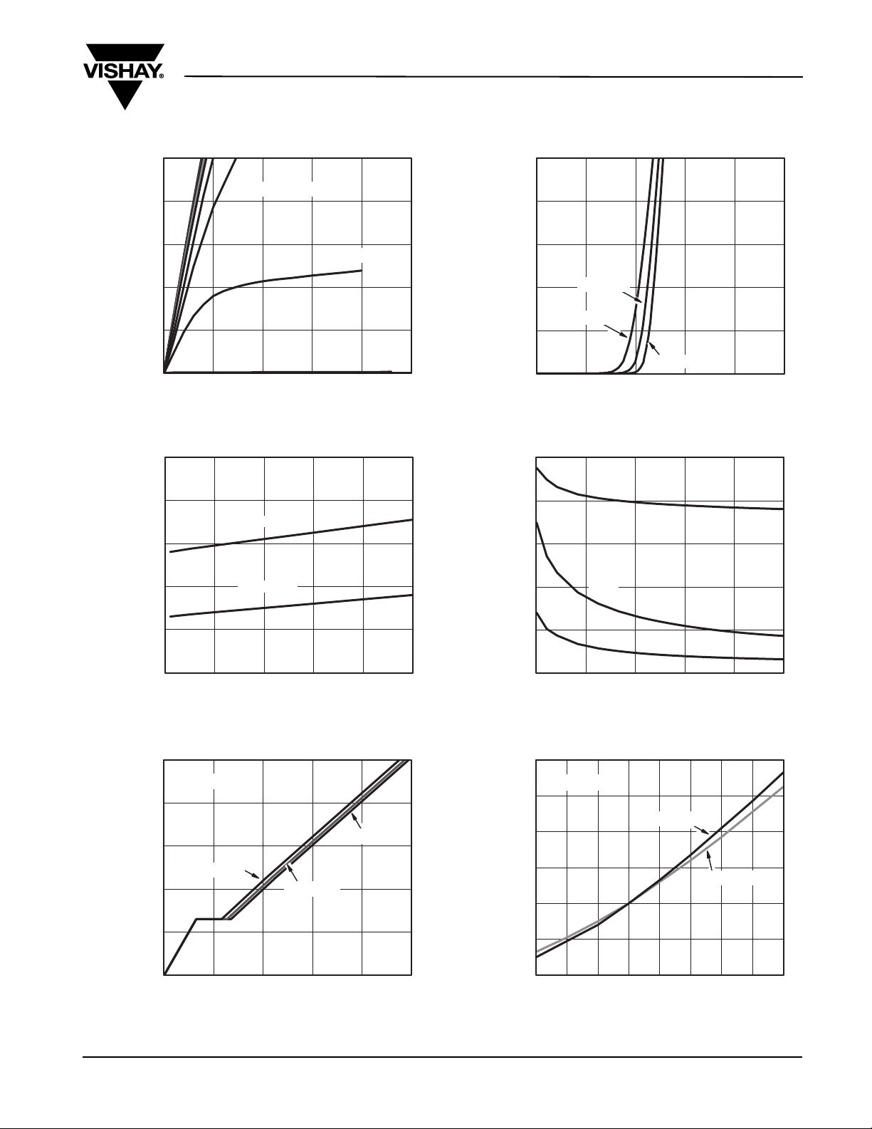
50
40
30
20
- Drain Current (A)I
D
10
0
0.0 0.5 1.0 1.5 2.0 2.5
VGS=10thru 4 V
- Drain-to-Source Voltage (V)
V
DS
Output Characteristics
0.015
0.013
VGS=4.5V
0.011
VGS=3V
8.0
6.4
4.8
3.2
- Drain Current (A)I
D
1.6
0.0
012345
TC= 25 °C
TC= 125 °C
V
GS
TC= - 55 °C
- Gate-to-Source Voltage (V)
Transfer Characteristics
1300
C
iss
1040
780
- On-Resistance (Ω)R
0.009
DS(on)
0.007
0.005
0 1020304050
VGS=10V
ID- Drain Current (A)
On-Resistance vs. Drain Current and Gate Voltage
10
ID=10A
8
6
VDS=10V
4
- Gate-to-Source Voltage (V)
GS
2
V
0
0.0 3.7 7.4 11.1 14.8 18.5
Qg- Total Gate Charge (nC)
VDS=15V
VDS=20V
Gate Charge
520
C - Capacitance (pF)
260
C
0
0 2.4 4.8 7.2 9.6 12
C
oss
rss
VDS- Drain-to-Source Voltage (V)
Capacitance
1.8
1.6
1.4
1.2
- On-Resistance
(Normalized)
1.0
DS(on)
R
0.8
0.6
ID=10A
VGS=10V
- 50 - 25 0 25 50 75 100 125 150
-Junction Temperature (°C)
T
J
On-Resistance vs. Junction Temperature
VGS=4.5V
Document Number: 68998
S-82773-Rev. A, 17-Nov-08
www.vishay.com
3
Page 4

New Product
Si4174DY
Vishay Siliconix
TYPICAL CHARACTERISTICS 25 °C, unless otherwise noted
100
10
1
0.1
- Source Current (A)I
S
0.01
0.001
0.0 0.2 0.4 0.6 0.8 1.0 1.2
TJ= 150 °C
VSD-Source-to-Drain Voltage (V)
Source-Drain Diode Forward Voltage
0.4
0.2
0
- 0.2
Variance (V)V
GS(th)
- 0.4
ID= 250 µA
- 0.6
TJ= 25 °C
ID=5mA
0.05
ID=10A
0.04
0.03
0.02
- On-Resistance (Ω)R
DS(on)
0.01
0.00
012345678 910
VGS- Gate-to-Source Voltage (V)
TJ= 125 °C
TJ=25 °C
On-Resistance vs. Gate-to-Source Voltage
80
64
48
32
Power (W)
16
- 0.8
- 50 - 25 0 25 50 75 100 125 150
www.vishay.com
4
TJ- Temperature (°C)
Threshold Voltage
- Drain Current (A)
D
I
0
Single Pulse Power, Junction-to-Ambient
100
Limited byR
10
1
0.1
TA= 25 °C
Single Pulse
0.01
0.1 1 10 100
V
DS
* V
> minimum VGSat which R
GS
*
DS(on)
BVDSS Limited
- Drain-to-Source Voltage (V)
DS(on)
1ms
10 ms
100 ms
1s
10 s
DC
is specified
Safe Operating Area, Junction-to-Ambient
011100.0 0.01 0.1
Time (s)
Document Number: 68998
S-82773-Rev. A, 17-Nov-08
Page 5

New Product
TYPICAL CHARACTERISTICS 25 °C, unless otherwise noted
20
16
12
8
- Drain Current (A)
D
I
4
0
0 25 50 75 100 125 150
- Case Temperature (°C)
T
C
Current Derating*
Si4174DY
Vishay Siliconix
6.0
4.8
3.6
Power (W)
2.4
1.2
0.0
0 25 50 75 100 125 150
- Case Temperature (°C)
T
C
Power, Junction-to-Ambient
* The power dissipation PD is based on T
dissipation limit for cases where additional heatsinking is used. It is used to determine the current rating, when this rating falls below the package
= 150 °C, using junction-to-case thermal resistance, and is more useful in settling the upper
J(max)
2.0
1.6
1.2
Power (W)
0.8
0.4
0.0
0 25 50 75 100 125 150
-Ambient Temperature (°C)
T
A
Power Derating, Junction-to-Foot
limit.
Document Number: 68998
S-82773-Rev. A, 17-Nov-08
www.vishay.com
5
Page 6

New Product
Si4174DY
Vishay Siliconix
TYPICAL CHARACTERISTICS 25 °C, unless otherwise noted
1
Duty Cycle = 0.5
0.2
Thermal Impedance
Normalized Effective Transient
Thermal Impedance
Normalized Effective Transient
0.1
0.01
10
1
0.1
0.01
10
0.1
0.05
0.02
-4
Duty Cycle = 0.5
0.2
0.1
Single Pulse
-4
-3
10
Single Pulse
-2
10
-1
1
Square WavePulse Duration (s)
Normalized Thermal Transient Impedance, Junction-to-Ambient
0.05
0.02
-3
10
-2
10
-1
Square WavePulse Duration (s)
Normalized Thermal Transient Impedance, Junction-to-Foot
Notes:
P
DM
1. Duty Cycle, D =
2. Per Unit Base = R
3. T
JM-TA=PDMZthJA
4. Surface Mounted
10
t
1
t
2
t
1
t
2
= 85 °C/W
thJA
(t)
100
100010
01110
Vishay Siliconix maintains worldwide manufacturing capability. Products may be manufactured at one of several qualified locations. Reliability data for Silicon
Technology and Package Reliability represent a composite of all qualified locations. For related documents such as package/tape drawings, part marking, and
reliability data, see http://www.vishay.com/ppg?68998.
www.vishay.com
6
Document Number: 68998
S-82773-Rev. A, 17-Nov-08
Page 7

SOIC (NARROW): 8-LEAD
JEDEC Part Number: MS-012
Package Information
Vishay Siliconix
D
e
BA
1
DIM
A 1.35 1.75 0.053 0.069
A
1
B 0.35 0.51 0.014 0.020
C 0.19 0.25 0.0075 0.010
D 4.80 5.00 0.189 0.196
E 3.80 4.00 0.150 0.157
e 1.27 BSC 0.050 BSC
H 5.80 6.20 0.228 0.244
h 0.25 0.50 0.010 0.020
L 0.50 0.93 0.020 0.037
q0°8°0°8°
S 0.44 0.64 0.018 0.026
ECN: C-06527-Rev. I, 11-Sep-06
DWG: 5498
8
1
0.25 mm (Gage Plane)
A
6
7
2
5
HE
3
4
S
h x 45
C
L
MILLIMETERS INCHES
Min Max Min Max
0.10 0.20 0.004 0.008
All Leads
q
0.101 mm
0.004"
Document Number: 71192
11-Sep-06
www.vishay.com
1
Page 8

Application Note 826
Vishay Siliconix
RECOMMENDED MINIMUM PADS FOR SO-8
0.172
(4.369)
0.028
(0.711)
Return to Index
Return to Index
0.022
(0.559)
0.246
(6.248)
Recommended Minimum Pads
Dimensions in Inches/(mm)
0.050
(1.270)
0.152
0.047
(3.861)
(1.194)
APPLICATION NOTE
www.vishay.com Document Number: 72606
22 Revision: 21-Jan-08
Page 9

Legal Disclaimer Notice
www.vishay.com
Vishay
Disclaimer
ALL PRODUCT, PRODUCT SPECIFICATIONS AND DATA ARE SUBJECT TO CHANGE WITHOUT NOTICE TO IMPROVE
RELIABILITY, FUNCTION OR DESIGN OR OTHERWISE.
Vishay Intertechnology, Inc., its affiliates, agents, and employees, and all persons acting on its or their behalf (collectively,
“Vishay”), disclaim any and all liability for any errors, inaccuracies or incompleteness contained in any datasheet or in any other
disclosure relating to any product.
Vishay makes no warranty, representation or guarantee regarding the suitability of the products for any particular purpose or
the continuing production of any product. To the maximum extent permitted by applicable law, Vishay disclaims (i) any and all
liability arising out of the application or use of any product, (ii) any and all liability, including without limitation special,
consequential or incidental damages, and (iii) any and all implied warranties, including warranties of fitness for particular
purpose, non-infringement and merchantability.
Statements regarding the suitability of products for certain types of applications are based on Vishay’s knowledge of
typical requirements that are often placed on Vishay products in generic applications. Such statements are not binding
statements about the suitability of products for a particular application. It is the customer’s responsibility to validate that a
particular product with the properties described in the product specification is suitable for use in a particular application.
Parameters provided in datasheets and / or specifications may vary in different applications and performance may vary over
time. All operating parameters, including typical parameters, must be validated for each customer application by the customer’s
technical experts. Product specifications do not expand or otherwise modify Vishay’s terms and conditions of purchase,
including but not limited to the warranty expressed therein.
Except as expressly indicated in writing, Vishay products are not designed for use in medical, life-saving, or life-sustaining
applications or for any other application in which the failure of the Vishay product could result in personal injury or death.
Customers using or selling Vishay products not expressly indicated for use in such applications do so at their own risk.
Please contact authorized Vishay personnel to obtain written terms and conditions regarding products designed for
such applications.
No license, express or implied, by estoppel or otherwise, to any intellectual property rights is granted by this document
or by any conduct of Vishay. Product names and markings noted herein may be trademarks of their respective owners.
© 2017 VISHAY INTERTECHNOLOGY, INC. ALL RIGHTS RESERVED
Revision: 08-Feb-17
1
Document Number: 91000
 Loading...