

Si1869DH
查询"Si1869DH"供应商
Load Switch with Level-Shift
PRODUCT SUMMARY
V
(V) R
DS2
0.165 at V
1.8 to 20
0.222 at V
0.303 at V
DESCRIPTION
The Si1869DH includes a p- and n-channel MOSFET in a
single SC70-6 package. The low on-resistance p-channel
TrenchFET is tailored for use as a load switch. The
n-channel, with an external resistor, can be used as a levelshift to drive the p-channel load-switch. The n-channel
MOSFET has internal ESD protection and can be driven by
logic signals as low as 1.5 V. The Si1869DH operates on
supply lines from 1.8 V to 20 V, and can drive loads up to
1.2 A.
(Ω)I
DS(on)
= 4.5 V ± 1.2
IN
= 2.5 V ± 1.0
IN
= 1.8 V ± 0.7
IN
D
(A)
Vishay Siliconix
FEATURES
• Halogen-free According to IEC 61249-2-21
Definition
• TrenchFET
• ESD Protected: 2000 V On Input Switch,
V
ON/OFF
• 165 mΩ Low R
• 1.8 to 20 V Input
• 1.5 to 8 V Logic Level Control
• Low Profile, Small Footprint SC70-6 Package
• Adjustable Slew-Rate
• Compliant to RoHS Directive 2002/95/EC
APPLICATIONS
• Level Shift for Portable Devices
®
Power MOSFETs: 1.8 V Rated
DS(on)
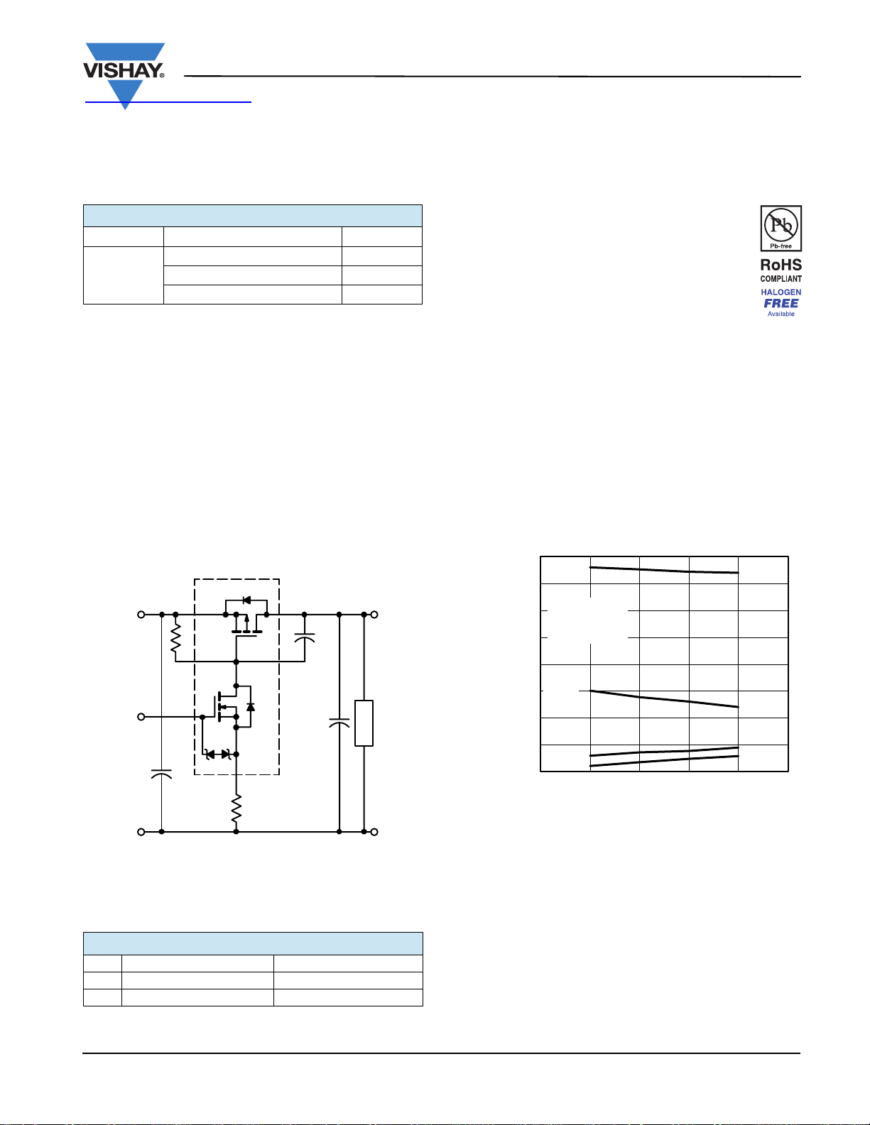
APPLICATION CIRCUITS
Si1869DH
V
ON/OFF
R2
IN
R1
C
i
4
Q2
6
5
Q1
1
R2
2, 3
6
40
t
35
IL = 1 A
(Time µs)
30
25
20
15
10
5
0
02468 10
= 3 V
V
ON/OFF
C
= 10 µF
i
= 1 µF
C
o
t
d(off)
t
r
R2 (kΩ)
Note: For R2 switching variations with other VIN/R1
combinations see Typical Characteristics
V
OUT
C1
C
o
LOAD
GND
f
t
d(on)
Switching Variation
R2 at V
= 2.5 V, R1 = 20 kΩ
IN
COMPONENTS
R1 Pull-Up Resistor Typical 10 kΩ to 1 MΩ*
R2 Optional Slew-Rate Control Typical 0 to 100 kΩ*
C1 Optional Slew-Rate Control Typical 1000 pF
* Minimum R1 value should be at least 10 x R2 to ensure Q1 turn-on.
Document Number: 73449
S10-0792-Rev. C, 05-Apr-10
The Si1869DH is ideally suited for high-side load switching in
portable applications. The integrated n-channel level-shift
device saves space by reducing external components. The
slew rate is set externally so that rise-times can be tailored to
different load types.
www.vishay.com
1
Si1869DH
SC
查询"Si1869DH"供应商
Vishay Siliconix
FUNCTIONAL BLOCK DIAGRAM
70-6
To p View
R2
D2
D2
1
2
3
6
5
4
R1, C1
ON/OFF
S2
Marking Code
VC XX
YY
Lot T raceability
and Date Code
Part # Code
S2
ON/OFF
Si1869DH
4
5
Q2
Q1
2, 3
D2
6
R1,
C1
Ordering Information: Si1869DH-T1-E3 (Lead (Pb)-free)
Si1869DH-T1-GE3 (Lead (Pb)-free and Halogen-free)
R2
1
ABSOLUTE MAXIMUM RATINGS TA = 25 °C, unless otherwise noted
Parameter Symbol Limit Unit
Drain-Source Voltage (D2-S2) V
ON/OFF Voltage V
Load Current
Continuous Intrinsic Diode Conduction
Maximum Power Dissipation
a
Continuous
a
a, b
b, c
Operating Junction and Storage Temperature Range T
ESD Rating, MIL-STD-883D Human Body Model (100 pF, 1500 Ω)
DS
IN
ON/OFF
I
L
I
S
P
D
, T
J
stg
ESD
- 20
20
8
± 1.2
± 3
- 0.4
1.0
- 55 to 150
2
VInput Voltage V
APulsed
W
°C
kV
THERMAL RESISTANCE RATINGS
Parameter Symbol Typical Maximum Unit
Maximum Junction-to-Ambient (Continuous Current)
a
Maximum Junction-to-Foot (Q2) R
R
thJA
thJF
100 125
44 55
°C/W
SPECIFICATIONS TJ = 25 °C unless otherwise noted
Parameter Symbol Test Conditions Min. Typ. Max. Unit
OFF Characteristics
Reverse Leakage Current I
Diode Forward Voltage V
FL
SD
VIN = 8 V, V
IS = - 0.4 A 0.4 0.6 1.1 V
ON Characteristics
Input Voltage Range V
Drain to Source Breakdown Voltage
On-Resistance (P-Channel) at 1 A R
On-State (P-Channel) Drain-Current I
Notes:
IN
V
DS
DS(on)
D(on)
VGS = 0 V, ID = - 250 µA- 20
V
= 1.5 V, VIN = 4.5 V, ID = 1.2 A 0.132 0.165
ON/OFF
= 1.5 V, VIN = 2.5 V, ID = 1.0 A 0.177 0.222
ON/OFF
= 1.5 V, VIN = 1.8 V, ID = 0.7 A 0.242 0.303
V
ON/OFF
V
≤ 0.2 V, VIN = 5 V, V
IN-OUT
V
≤ 0.3 V, VIN = 3 V, V
IN-OUT
a. Surface mounted on FR4 board.
= 20 V, V
b. V
IN
c. Pulse test: pulse width ≤ 300 µs, duty cycle ≤ 2 %.
Stresses beyond those listed under “Absolute Maximum Ratings” may cause permanent damage to the device. These are stress ratings only, and functional operation
of the device at these or any other conditions beyond those indicated in the operational sections of the specifications is not implied. Exposure to absolute maximum
rating conditions for extended periods may affect device reliability.
= 8 V, TA = 25 °C.
ON/OFF
= 0 V 1 µA
ON/OFF
1.8 20
= 1.5 V 1
ON/OFF
= 1.5 V 1
ON/OFF
V
ΩV
A
www.vishay.com
2
Document Number: 73449
S10-0792-Rev. C, 05-Apr-10

Si1869DH
查询"Si1869DH"供应商
TYPICAL CHARACTERISTICS 25 °C, unless otherwise noted
0.6
V
= 1.5 V to 8 V
ON/OFF
0.5
0.4
(V)V
0.3
DROP
0.2
0.1
0.0
0.0 0.5 1.0 1.5 2.0 2.5 3.0
0.6
V
ON/OFF
0.5
TJ = 125 °C
V
vs. IL at VIN = 4.5 V
DROP
= 1.5 V to 8 V
TJ = 25 °C
IL (A)
Vishay Siliconix
0.6
V
= 1.5 V to 8 V
ON/OFF
0.5
0.4
(V)V
0.3
DROP
0.2
0.1
0.0
0.0 0.5 1.0 1.5 2.0 2.5
0.5
0.4
TJ = 125 °C
V
vs. IL at VIN = 2.5 V
DROP
TJ = 25 °C
(A)
I
L
V
ON/OFF
= 1.5 V to 8 V
0.4
(V)V
0.3
DROP
0.2
0.1
0.0
0.0 0.2 0.4 0.6 0.
0.10
IL = 0.7 A
V
ON/OFF
0.06
0.02
Variance (V)
- 0.02
DROP
V
- 0.06
TJ = 125 °C
V
vs. IL at VIN = 1.8 V
DROP
= 1.5 V to 8 V
TJ = 25 °C
8 1.0 1.2 1.4 1.6
IL (A)
VIN = 1.8 V
VIN = 4.5 V
0.3
(V)V
DROP
0.2
0.1
0.0
0123456
V
0.5
0.4
0.3
0.2
- On-Resistance (Ω)
SS(on)
R
0.1
TJ = 125 °C
TJ = 25 °C
VIN (V)
vs. VIN at IL = 0.7 A
DROP
IL = 0.7 A
V
TJ = 125 °C
TJ = 25 °C
ON/OFF
= 1.5 V to 8 V
- 0.10
- 50 - 25 0 25 50 75 100 125 150
Variance vs. Junction Temperature
V
DROP
Document Number: 73449
S10-0792-Rev. C, 05-Apr-10
TJ- Junction Temperature (°C)
0.0
0123456
(V)
V
IN
On-Resistance vs. Input Voltage
www.vishay.com
3

Si1869DH
200
查询"Si1869DH"供应商
Vishay Siliconix
TYPICAL CHARACTERISTICS 25 °C, unless otherwise noted
1.6
IL = 0.7 A
V
= 1.5 V to 8 V
ON/OFF
1.4
1.2
- On-Resistance
1.0
(Normalized)
DS(on)
R
0.8
0.6
- 50 - 25 0 25 50 75 100 125 150
TJ- Junction Temperature (°C)
Normalized On-Resistance
vs. Junction Temperature
VIN = 4.5 V
VIN = 1.8 V
20
t
µs)
(Time
16
t
= 3 V
t
r
t
d(on)
f
12
IL = 1 A
V
ON/OFF
C
= 10 µF
8
i
C
= 1 µF
o
4
0
02468 10
R2 (kΩ)
Switching Variation
R2 at V
= 4.5 V, R1 = 20 kΩ
IN
d(off)
(
Time µs)
µs)
(Time
40
35
IL = 1 A
V
ON/OFF
C
= 10 µF
i
C
= 1 µF
o
= 3 V
30
25
20
t
d(off)
15
10
5
t
r
t
0
02468 10
R2 (kΩ)
Switching Variation
R2 at V
250
200
150
IL = 1 A
= 3 V
V
ON/OFF
C
= 10 µF
i
C
= 1 µF
o
100
50
0
0 20406080 100
= 2.5 V, R1 = 20 kΩ
IN
R2 (kΩ)
Switching Variation
R2 at V
= 4.5 V, R1 = 300 kΩ
IN
t
f
d(on)
t
d(off)
t
f
t
r
t
d(on)
100
80
IL = 1 A
= 3 V
V
ON/OFF
60
= 10 µF
C
i
= 1 µF
(Time µs)
C
o
40
t
d(off)
20
t
0
r
02468 10
R2 (kΩ)
Switching Variation
R2 at V
t
d(off)
µs)
(Time
150
100
I L = 1 A
V
ON/OFF
C
= 10 µF
i
C
= 1 µF
o
t
f
50
t
d(on)
t
0
r
0 20406080 100
= 1.8 V, R1 = 20 kΩ
IN
= 3 V
R2 (kΩ)
Switching Variation
R2 at V
= 2.5 V, R1 = 300 kΩ
IN
t
d(on)
t
f
www.vishay.com
4
Document Number: 73449
S10-0792-Rev. C, 05-Apr-10

Si1869DH
查询"Si1869DH"供应商
TYPICAL CHARACTERISTICS 25 °C, unless otherwise noted
200
t
d(off)
IL = 1 A
150
V
= 3 V
ON/OFF
C
= 10 µF
i
C
= 1 µF
o
t
f
50
t
d(on)
t
0
r
020406080100
R2 (kΩ)
Switching Variation
R2 at V
= 1.8 V, R1 = 300 kΩ
IN
2
1
Duty Cycle = 0.5
(Time µs)
100
Vishay Siliconix
Transient
0.1
Thermal Impedance
Normalized Effective
0.01
10
2
1
0.1
Thermal Impedance
Normalized Effective Transient
0.2
0.1
0.05
0.02
Single Pulse
-4
Duty Cycle = 0.5
0.2
0.1
0.05
0.02
Single Pulse
Notes:
P
DM
t
1
t
2
t
thJA
t
thJA
100
1
2
(t)
= 100 °C/W
00601110
1. Duty Cycle, D =
2. Per Unit Base = R
3. T
- TA = PDMZ
JM
4. Surface Mounted
-3
10
-2
10
-1
Square Wave Pulse Duration (s)
Normalized Thermal Transient Impedance, Junction-to-Ambient
0.01
-4
10
-3
10
-2
10
-1
01110
Square Wave Pulse Duration (s)
Normalized Thermal Transient Impedance, Junction-to-Foot
Vishay Siliconix maintains worldwide manufacturing capability. Products may be manufactured at one of several qualified locations. Reliability data for Silicon
Technology and Package Reliability represent a composite of all qualified locations. For related documents such as package/tape drawings, part marking, and
reliability data, see www.vishay.com/ppg?73449
Document Number: 73449
.
www.vishay.com
S10-0792-Rev. C, 05-Apr-10
5

Legal Disclaimer Notice
查询"Si1869DH"供应商
Vishay
Disclaimer
All product specifications and data are subject to change without notice.
Vishay Intertechnology, Inc., its affiliates, agents, and employees, and all persons acting on its or their behalf
(collectively, “Vishay”), disclaim any and all liability for any errors, inaccuracies or incompleteness contained herein
or in any other disclosure relating to any product.
Vishay disclaims any and all liability arising out of the use or application of any product described herein or of any
information provided herein to the maximum extent permitted by law. The product specifications do not expand or
otherwise modify Vishay’s terms and conditions of purchase, including but not limited to the warranty expressed
therein, which apply to these products.
No license, express or implied, by estoppel or otherwise, to any intellectual property rights is granted by this
document or by any conduct of Vishay.
The products shown herein are not designed for use in medical, life-saving, or life-sustaining applications unless
otherwise expressly indicated. Customers using or selling Vishay products not expressly indicated for use in such
applications do so entirely at their own risk and agree to fully indemnify Vishay for any damages arising or resulting
from such use or sale. Please contact authorized Vishay personnel to obtain written terms and conditions regarding
products designed for such applications.
Product names and markings noted herein may be trademarks of their respective owners.
Document Number: 91000 www.vishay.com
Revision: 18-Jul-08 1
 Loading...