

SFH690ABT, SFH690AT, SFH690BT, SFH690CT, SFH690DT
i179065_3
1
2
4
3
E
C
A
C
V
DE
i179066
www.vishay.com
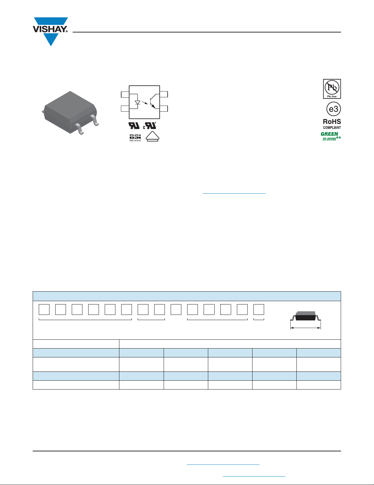
Optocoupler Phototransistor Output, SOP-4,
100 mil Pitch, Mini-Flat Package
DESCRIPTION
The SFH690ABT, SFH690AT, SFH690BT, SFH690CT,
SFH690DT family has a GaAs infrared emitting diode
emitter, which is optically coupled to a silicon planar
phototransistor detector, and is incorporated in a 4 pin
100 mil lead pitch miniflat package. It features a high current
transfer ratio, low coupling capacitance, and high isolation
voltage.
The coupling devices are designed for signal transmission
between two electrically separated circuits. The SFH690
series is available only on tape and reel. There are
2000 parts per reel. Marking for SFH690AT is 690A;
SFH690BT is 690B; SFH690CT is 690C; SFH690DT is 690D;
SFH690ABT will be marked as 690A or 690B.
Vishay Semiconductors
FEATURES
• SOP (small outline package)
• Isolation test voltage, 3750 V
• High collector emitter breakdown voltage,
V
= 70 V
CEO
• Low saturation voltage
• Fast switching times
• Temperature stable
• Low coupling capacitance
• End-stackable, 0.100" (2.54 mm) spacing
• Compliant to RoHS Directive 2002/95/EC and in
accordance to WEEE 2002/96/EC
Note
** Please see document “Vishay Material Category Policy”:
www.vishay.com/doc?99902
APPLICATIONS
• High density mounting or space sensitive PCBs
•PLCs
• Telecommunication
AGENCY APPROVALS
• UL1577, file no. E52744 system code U
• cUL tested to CSA 22.2 bulletin 5A
• BSI IEC 60950; IEC 60065
• DIN EN 60747-5-2 (VDE 0884) available with option 1
RMS
(1 s)
ORDERING INFORMATION
SFH690xx-X001T
PART NUMBER CTR
AGENCY CERTIFIED/PACKAGE CTR (%)
UL, cUL, BSI 50 to 300 50 to 150 100 to 300 100 to 200 200 to 400
SOP-4, 100 mil pitch SFH690ABT
VDE, UL, cUL, BSI 50 to 300 50 to 150 100 to 300 100 to 200 200 to 400
SOP-4, 100 mil pitch - - - SFH690C-X001T SFH690D-X001T
Notes
(1)
Product is rotated 180° in tape and reel cavity
(2)
Also available in tubes, do not put “T” to the end
Rev. 2.3, 13-Sep-11
For technical questions, contact: optocoupleranswers@vishay.com
THIS DOCUMENT IS SUBJECT TO CHANGE WITHOUT NOTICE. THE PRODUCTS DESCRIBED HEREIN AND THIS DOCUMENT
ARE SUBJECT TO SPECIFIC DISCLAIMERS, SET FORTH AT www.vishay.com/doc?91000
BIN
SFH690AT3
SFH690AT
PACKAGE OPTION TAPE
(1)
,
SFH690BT3
(2)
1
SFH690BT
AND
REEL
(1)
,
(2)
SFH690CT SFH690DT
SOP-#
7.21 mm
Document Number: 83686
SFH690ABT, SFH690AT, SFH690BT, SFH690CT, SFH690DT
www.vishay.com
Vishay Semiconductors
ABSOLUTE MAXIMUM RATINGS (T
= 25 °C, unless otherwise specified)
amb
PARAMETER TEST CONDITION SYMBOL VALUE UNIT
INPUT
Reverse voltage V
DC forward current I
Surge forward current t
10 μs I
p
Power dissipation P
R
F
FSM
diss
6V
50 mA
2.5 A
80 mW
OUTPUT
Collector emitter voltage V
Emitter collector voltage V
Collector current
t
1 ms I
p
Power dissipation P
CEO
ECO
I
C
C
diss
70 V
7V
50 mA
100 mA
150 mW
COUPLER
Isolation test voltage between emitter and
detector (1 s)
Isolation resistance
= 500 V, T
IO
V
= 500 V, T
IO
= 25 °C R
amb
= 100 °C R
amb
V
Storage temperature range T
Ambient temperature range T
Soldering temperature
(1)
max. 10 s dip soldering distance to
seating plane 1.5 mm
V
T
ISO
IO
IO
stg
amb
sld
3750 V
12
10
11
10
RMS
- 55 to + 150 °C
- 55 to + 100 °C
260 °C
Notes
• Stresses in excess of the absolute maximum ratings can cause permanent damage to the device. Functional operation of the device is not
implied at these or any other conditions in excess of those given in the operational sections of this document. Exposure to absolute
maximum ratings for extended periods of the time can adversely affect reliability.
(3)
Refer to reflow profile for soldering conditions for surface mounted devices.
200
150
100
50
- Power Dissipation (mW)
tot
P
18484
Diode
0
0 255075100125150
T
- Ambient Temperature (°C)
amb
Phototransistor
Fig. 1 - Permissible Power Dissipation vs. Ambient Temperature
Rev. 2.3, 13-Sep-11
2
Document Number: 83686
For technical questions, contact: optocoupleranswers@vishay.com
THIS DOCUMENT IS SUBJECT TO CHANGE WITHOUT NOTICE. THE PRODUCTS DESCRIBED HEREIN AND THIS DOCUMENT
ARE SUBJECT TO SPECIFIC DISCLAIMERS, SET FORTH AT www.vishay.com/doc?91000
SFH690ABT, SFH690AT, SFH690BT, SFH690CT, SFH690DT
www.vishay.com
Vishay Semiconductors
ELECTRICAL CHARACTERISTICS (T
= 25 °C, unless otherwise specified)
amb
PARAMETER TEST CONDITION SYMBOL MIN. TYP. MAX. UNIT
INPUT
Forward voltage I
Reverse current V
Capacitance V
Thermal resistance R
= 5 mA V
F
= 6 V I
R
= 0 V, f = 1 MHz C
R
F
R
O
thJA
1.15 1.4 V
0.01 10 μA
14 pF
750 K/W
OUTPUT
Collector emitter leakage current V
Collector emitter capacitance V
Thermal resistance R
= 20 V I
CE
= 5 V, f = 1 MHz C
CE
CEO
CE
thJA
100 nA
2.8 pF
500 K/W
COUPLER
Collector emitter saturation voltage I
Coupling capacitance f = 1 MHz C
= 10 mA, IC = 2 mA V
F
CEsat
C
0.1 0.3 V
0.3 pF
Note
• Minimum and maximum values are testing requirements. Typical values are characteristics of the device and are the result of engineering
evaluation. Typical values are for information only and are not part of the testing requirements.
CURRENT TRANSFER RATIO (T
= 25 °C, unless otherwise specified)
amb
PARAMETER TEST CONDITION PART SYMBOL MIN. TYP. MAX. UNIT
SFH690ABT CTR 50 300 %
SFH690AT CTR 50 150 %
I
C/IF
IF = 5 mA, VCE = 5 V
SFH690BT CTR 100 300 %
SFH690CT CTR 100 200 %
SFH690DT CTR 200 400 %
SWITCHING CHARACTERISTICS (T
= 25 °C, unless otherwise specified)
amb
PARAMETER TEST CONDITION SYMBOL MIN. TYP. MAX. UNIT
Rise time I
Fall time I
Turn-on time I
Turn-off time I
= 2 mA, VCC = 5 V, RL = 100 t
C
= 2 mA, VCC = 5 V, RL = 100 t
C
= 2 mA, VCC = 5 V, RL = 100 t
C
= 2 mA, VCC = 5 V, RL = 100 t
C
I
F
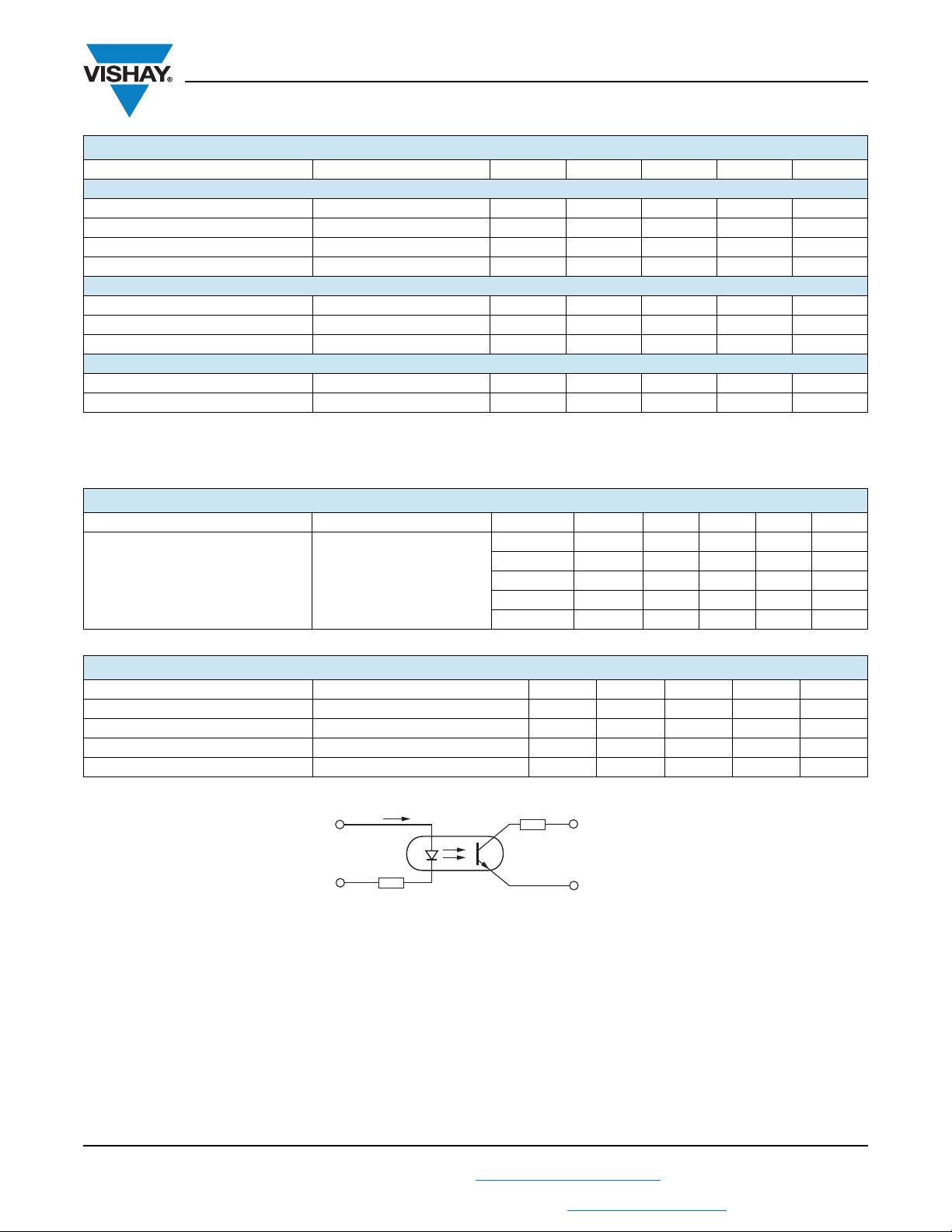
isfh690at_01
50 Ω
RL=100 Ω
r
f
on
off
3μs
4μs
5μs
3μs
VCC=5V
Fig. 2 - Switching Operation (without Saturation)
Rev. 2.3, 13-Sep-11
3
Document Number: 83686
For technical questions, contact: optocoupleranswers@vishay.com
THIS DOCUMENT IS SUBJECT TO CHANGE WITHOUT NOTICE. THE PRODUCTS DESCRIBED HEREIN AND THIS DOCUMENT
ARE SUBJECT TO SPECIFIC DISCLAIMERS, SET FORTH AT www.vishay.com/doc?91000

0.6
0.7
0.8
0.9
1.0
1.1
1.2
1.3
1.4
1.5
1.6
0.1 1 10 100
V
F
- Forward Voltage (V)
IF- Forward Current (mA)
T
amb
= 25 °C
T
amb
= 75 °C
T
amb
= 100 °C
T
amb
= 0 °C
T
amb
= - 55 °C
0
2
4
6
8
10
12
14
00.10.20.30.4
I
C
- Collector Current (mA)
VCE- Collector Emitter Voltage (sat) (V)
IF= 1 mA
IF= 10 mA
IF= 5 mA
IF= 2 mA
SFH690ABT, SFH690AT, SFH690BT, SFH690CT, SFH690DT
www.vishay.com
SAFETY AND INSULATION RATINGS
PARAMETER TEST CONDITION SYMBOL MIN. TYP. MAX. UNIT
Climatic classification
(according to IEC 68 part 1)
Comparative tracking index CTI 175 399
V
IOTM
V
IORM
P
SO
I
SI
T
SI
Creepage distance 5 mm
Clearance distance 5 mm
Insulation thickness 0.4 mm
Note
• As per IEC 60747-5-2, §7.4.3.8.1, this optocoupler is suitable for “safe electrical insulation” only within the safety ratings. Compliance with
the safety ratings shall be ensured by means of protective circuits.
6000 V
707 V
Vishay Semiconductors
55/100/21
350 mW
150 mA
175 °C
TYPICAL CHARACTERISTICS (T
Fig. 3 - Forward Voltage vs. Forward Current
40
35
30
25
20
15
10
- Collector Current (mA)
C
5
Rev. 2.3, 13-Sep-11
I
0
012345678
VCE- Collector Emitter Voltage (NS) (V)
Fig. 4 - Collector Current vs. Collector Emitter Voltage (NS)
THIS DOCUMENT IS SUBJECT TO CHANGE WITHOUT NOTICE. THE PRODUCTS DESCRIBED HEREIN AND THIS DOCUMENT
= 25 °C, unless otherwise specified)
amb
10 000
1000
- Leakage Current (nA)
CE0
I
0.001
IF= 0 mA
100
10
1
0.1
0.01
- 60 - 40 - 20 0 20 40 60 80 100
T
- Ambient Temperature (°C)
amb
VCE= 40 V
Fig. 5 - Leakage Current vs. Ambient Temperature
IF= 20 mA
IF= 15 mA
IF= 10 mA
IF= 5 mA
Fig. 6 - Collector Current vs. Collector Emitter Voltage (sat)
4
For technical questions, contact: optocoupleranswers@vishay.com
ARE SUBJECT TO SPECIFIC DISCLAIMERS, SET FORTH AT www.vishay.com/doc?91000
VCE= 24 V
VCE= 12 V
Document Number: 83686

0
0.2
0.4
0.6
0.8
1.0
1.2
1.4
- 60 - 40 - 20 0 20 40 60 80 100
N
CTR
- Normalized CTR (NS)
T
amb
- Ambient Temperature (°C)
Normalized to:
I
F
= 5 mA, VCE= 5 V, T
amb
= 25 °C
IF= 10 mA
IF= 5 mA
IF= 1 mA
0
0.2
0.4
0.6
0.8
1.0
1.2
- 60 - 40 - 20 0 20 40 60 80 100
N
CTR
- Normalized CTR (sat)
T
amb
- Ambient Temperature (°C)
VCE=0.4 V
Normalized to:
I
F
= 5 mA, VCE= 5 V, T
amb
= 25 °C
IF= 5 mA
IF= 10 mA
IF= 1 mA
0
0.2
0.4
0.6
0.8
1.0
1.2
1.4
0.1 1 10 100
N
CTR
- Normalized CTR (NS)
IF- Forward Current (mA)
Normalized to:
I
F
= 5 A, VCE= 5 V,
T
amb
= 25 °C
T
amb
= 0 °C
T
amb
= 100 °C
T
amb
= 75 °C
T
amb
= - 55 °C
T
amb
= 25 °C
0
0.2
0.4
0.6
0.8
1.0
1.2
0.1 1 10 100
N
CTR
- Normalized CTR (sat)
IF- Forward Current (mA)
VCE= 0.4 V
Normalized to:
I
F
= 5 mA,
V
CE
= 5 V,
T
amb
= 25 °C
T
amb
= 0 °C
T
amb
= 75 °C
T
amb
= - 55 °C
T
amb
= 25 °C
T
amb
= 100 °C
- 160
- 140
- 120
- 100
-80
-60
-40
-20
0
1 10 100 1000
Phase (deg)
f (kHz)
VCE= 5 V
1
10
100
1000
0.1 1 10 100
F
CTR
(kHz)
IC(mA)
VCC= 5 V
SFH690ABT, SFH690AT, SFH690BT, SFH690CT, SFH690DT
www.vishay.com
Vishay Semiconductors
Fig. 7 - Normalized Current Transfer Ratio (sat) vs.
Ambient Temperature
Fig. 8 - Normalized Current Transfer Ratio (NS) vs.
Ambient Temperature
Fig. 10 - Normalized CTR (sat) vs. Forward Current
Fig. 11 - F
vs. Phase Angle
CTR
Rev. 2.3, 13-Sep-11
THIS DOCUMENT IS SUBJECT TO CHANGE WITHOUT NOTICE. THE PRODUCTS DESCRIBED HEREIN AND THIS DOCUMENT
Fig. 9 - Normalized CTR (NS) vs. Forward Current
Fig. 12 - F
5
For technical questions, contact: optocoupleranswers@vishay.com
ARE SUBJECT TO SPECIFIC DISCLAIMERS, SET FORTH AT www.vishay.com/doc?91000
vs. Collector Current
CTR
Document Number: 83686

SFH690ABT, SFH690AT, SFH690BT, SFH690CT, SFH690DT
0.1
1
10
100
1000
0.1 1 10 100
t
on
, t
off
Switching Time (μs)
RL-Load Resistance (kΩ)
t
off
t
on
VCE= 5 V, IF= 5 mA
i178037
4.83
4.32
4.67
4.17
0.61
0.86
1
4
2
3
0.46
0.36
2.67
2.41
Lead coplanarity
0.10 max.
0.46
0.33
0.63
0.38
5.59
5.08
40°
10°
0.20
0.10
7.21
6.71
2.03
1.91
6°
ISO method A
R 0.25
0.91
0.36
5.08
1.14
7.37
2.54
Pin one ID (on chamfer side of package)
690A
V YWW
U68X1
www.vishay.com
Fig. 13 - Switching Time vs. Load Resistance
PACKAGE DIMENSIONS in millimeters
Vishay Semiconductors
PACKAGE MARKING (example of SFH690AT)
Notes
• Only option 1 is reflected in the package marking with the characters “X1”
• Tape and reel suffix (T) is not part of the package marking
Rev. 2.3, 13-Sep-11
THIS DOCUMENT IS SUBJECT TO CHANGE WITHOUT NOTICE. THE PRODUCTS DESCRIBED HEREIN AND THIS DOCUMENT
For technical questions, contact: optocoupleranswers@vishay.com
ARE SUBJECT TO SPECIFIC DISCLAIMERS, SET FORTH AT www.vishay.com/doc?91000
6
Document Number: 83686

Legal Disclaimer Notice
www.vishay.com
Vishay
Disclaimer
ALL PRODUCT, PRODUCT SPECIFICATIONS AND DATA ARE SUBJECT TO CHANGE WITHOUT NOTICE TO IMPROVE
RELIABILITY, FUNCTION OR DESIGN OR OTHERWISE.
Vishay Intertechnology, Inc., its affiliates, agents, and employees, and all persons acting on its or their behalf (collectively,
“Vishay”), disclaim any and all liability for any errors, inaccuracies or incompleteness contained in any datasheet or in any other
disclosure relating to any product.
Vishay makes no warranty, representation or guarantee regarding the suitability of the products for any particular purpose or
the continuing production of any product. To the maximum extent permitted by applicable law, Vishay disclaims (i) any and all
liability arising out of the application or use of any product, (ii) any and all liability, including without limitation special,
consequential or incidental damages, and (iii) any and all implied warranties, including warranties of fitness for particular
purpose, non-infringement and merchantability.
Statements regarding the suitability of products for certain types of applications are based on Vishay’s knowledge of typical
requirements that are often placed on Vishay products in generic applications. Such statements are not binding statements
about the suitability of products for a particular application. It is the customer’s responsibility to validate that a particular
product with the properties described in the product specification is suitable for use in a particular application. Parameters
provided in datasheets and/or specifications may vary in different applications and performance may vary over time. All
operating parameters, including typical parameters, must be validated for each customer application by the customer’s
technical experts. Product specifications do not expand or otherwise modify Vishay’s terms and conditions of purchase,
including but not limited to the warranty expressed therein.
Except as expressly indicated in writing, Vishay products are not designed for use in medical, life-saving, or life-sustaining
applications or for any other application in which the failure of the Vishay product could result in personal injury or death.
Customers using or selling Vishay products not expressly indicated for use in such applications do so at their own risk. Please
contact authorized Vishay personnel to obtain written terms and conditions regarding products designed for such applications.
No license, express or implied, by estoppel or otherwise, to any intellectual property rights is granted by this document or by
any conduct of Vishay. Product names and markings noted herein may be trademarks of their respective owners.
Material Category Policy
Vishay Intertechnology, Inc. hereby certifies that all its products that are identified as RoHS-Compliant fulfill the
definitions and restrictions defined under Directive 2011/65/EU of The European Parliament and of the Council
of June 8, 2011 on the restriction of the use of certain hazardous substances in electrical and electronic equipment
(EEE) - recast, unless otherwise specified as non-compliant.
Please note that some Vishay documentation may still make reference to RoHS Directive 2002/95/EC. We confirm that
all the products identified as being compliant to Directive 2002/95/EC conform to Directive 2011/65/EU.
Vishay Intertechnology, Inc. hereby certifies that all its products that are identified as Halogen-Free follow Halogen-Free
requirements as per JEDEC JS709A standards. Please note that some Vishay documentation may still make reference
to the IEC 61249-2-21 definition. We confirm that all the products identified as being compliant to IEC 61249-2-21
conform to JEDEC JS709A standards.
Revision: 02-Oct-12
1
Document Number: 91000

 Loading...