

Page 1
SFH6700/ 01/ 02/ 05/ 11/ 12/ 19
High Speed Optocoupler, 5 MBd, 1 kV/µs dV/dt
Features
• Data Rate 5.0 MBits/s
(2.5 MBit/s over Temperature)
• Buffer
• Isolation Test Voltage, 5300 V RMS for 1.0 s
• TTL, LSTTL and CMOS Compatible
• Internal Shield for Very High Common Mode
Transient Immunity
• Wide Supply Voltage Range (4.5 to 15 V)
• Low Input Current (1.6 mA to 5.0 mA)
• Three State Output (SFH6700/ 19)
• Totem Pole Output (SFH6701/ 02/ 11/ 12)
• Open Collector Output (SFH6705)
• Lead (Pb)-free component
• Component in accordance to RoHS 2002/95/EC
and WEEE 2002/96/EC
e3
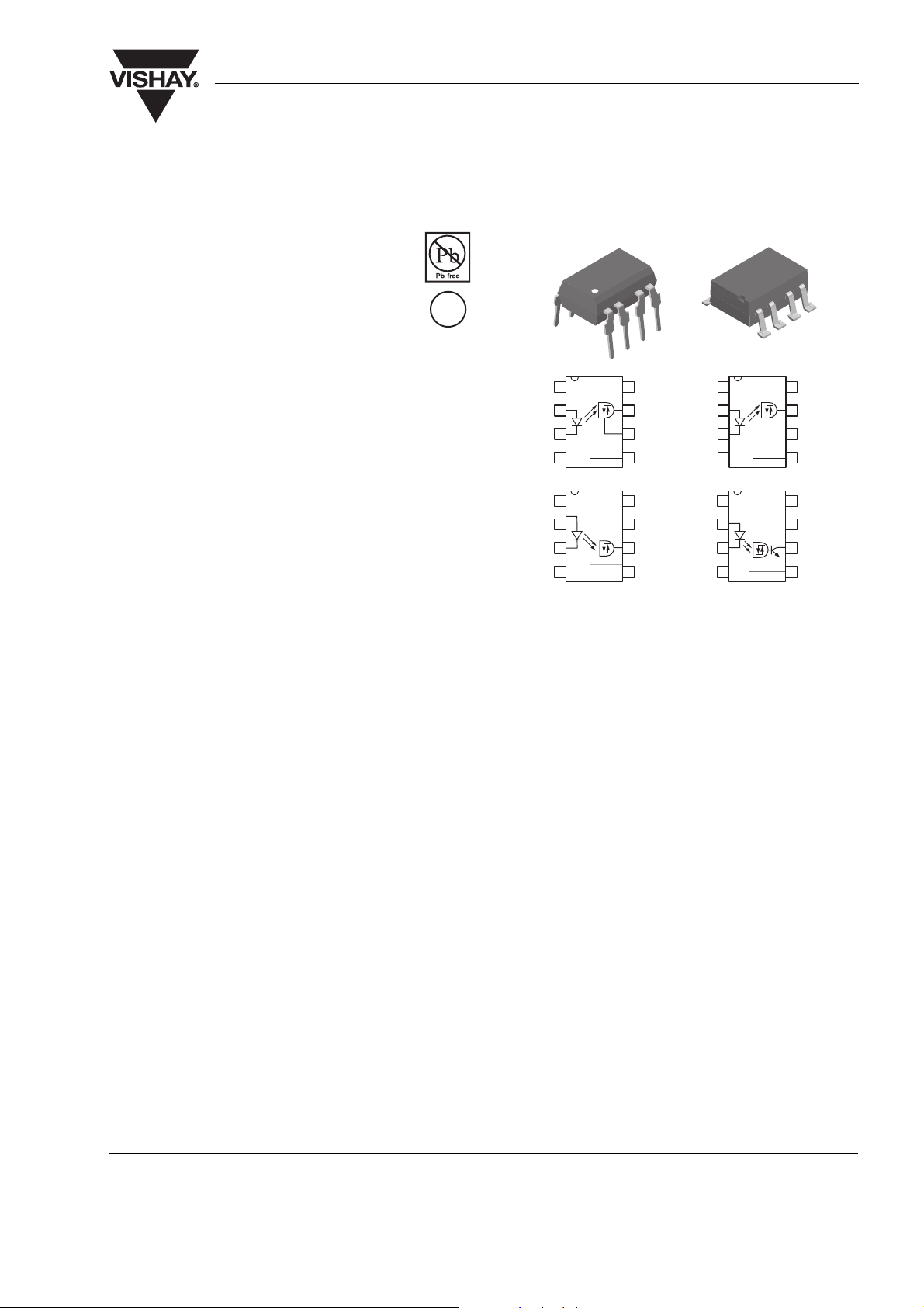
SFH6700/6719
1
NC
2
A
3
C
4
NC
SFH6702/6712
1
NC
2
A
3
C
NC
4
8
V
CC
V
7
O
V
6
E
GND
5
8
V
CC
NC
7
V
6
O
GND
5
Vishay Semiconductors
SFH6701/6711
i179073
NC
NC
NC
NC
A
C
A
C
1
2
3
4
SFH6705
1
2
3
4
8
V
CC
V
7
O
NC
6
GND
5
8
V
CC
NC
7
V
6
O
GND
5
Agency Approvals
• UL1577, File No. E52744 System Code H or J,
Double Protection
• DIN EN 60747-5-2 (VDE0884)
DIN EN 60747-5-5 pending
Available with Option 1
Applications
Industrial Control
Replace Pulse Transformers
Routine Logic Interfacing
Motion/Power Control
High Speed Line Receiver
Microprocessor System Interfaces
Computer Peripheral Interfaces
Description
The SFH67xx high speed optocoupler series consists
of a GaAlAs infrared emitting diode, optically coupled
with an integrated photo detector. The detector incorporates a Schmitt-Trigger stage for improved noise
immunity. Using the Enable input, the output can
switched to the high ohmic state, which is necessary
for data bus applications. A Faraday shield provides a
common mode transient immunity of 1000 V/µ at
V
= 50 V for SFH6700/ 01/ 02/ 05 and 2500 V/µ at
CM
V
= 400 V for SFH6711/ 12/ 19.
CM
The SFH67xx uses an industry standard DIP-8 package.With standard lead bending, creepage distance
and clearance of ≥ 7.0 mm with lead bending options
6, 7, and 9 ≥ 8 mm are achieved.
Document Number 83683
Rev. 1.5, 15-Apr-05
www.vishay.com
1
Page 2
SFH6700/ 01/ 02/ 05/ 11/ 12/ 19
Vishay Semiconductors
Order Information
Par t Remarks
SFH6700 Three State Output, DIP-8
SFH6701 Totem Pole Output, DIP-8
SFH6702 Totem Pole Output, DIP-8
SFH6705 Open Collector Output, DIP-8
SFH6711 Totem Pole Output, DIP-8
SFH6712 Totem Pole Output, DIP-8
SFH6719 Three State Output, DIP-8
SFH6700-X009 Three State Output, SMD-8 (option 9)
SFH6701-X006 Totem Pole Output, DIP-8 400 mil (option 6)
SFH6701-X007 Totem Pole Output, SMD-8 (option 7)
SFH6701-X009 Totem Pole Output, SMD-8 (option 9)
SFH6705-X006 Open Collector Output, DIP-8 400 mil (option
6)
SFH6705-X007 Open Collector Output, SMD-8 (option 7)
SFH6711-X007 Totem Pole Output, SMD-8 (option 7)
For additional information on the available options refer to
Option Information.
Truth Table (Positive Logic)
IR Diode Enable Output
SFH6700 on H Z
off H Z
SFH6719 on L H
off L L
SFH6701 on H
off L
SFH6702 on H
off L
SFH6705 on H
off L
SFH6711 on H
off L
SFH6712 on H
off L
Absolute Maximum Ratings
T
= 25 °C, unless otherwise specified
amb
Stresses in excess of the absolute Maximum Ratings can cause permanent damage to the device. Functional operation of the device is
not implied at these or any other conditions in excess of those given in the operational sections of this document. Exposure to absolute
Maximum Rating for extended periods of the time can adversely affect reliability.
Input
Parameter Test condition Symbol Value Unit
Reverse voltage V
DC Forward current I
Surge forward current t ≤ 1.0 µsI
Power dissipation P
R
F
FSM
diss
3.0 V
10 mA
1.0 A
20 mW
www.vishay.com
2
Document Number 83683
Rev. 1.5, 15-Apr-05
Page 3
SFH6700/ 01/ 02/ 05/ 11/ 12/ 19
Vishay Semiconductors
Output
Parameter Test condition Symbol Value Unit
Supply voltage V
Three state enable voltage
(SFH6700/19 only)
Output voltage V
Average output current I
Power dissipation P
CC
V
EN
O
O
diss
Coupler
Parameter Test condition Symbol Value Unit
Storage temperature range T
Ambient temperature range T
Lead soldering temperature t = 10 s T
Isolation test voltage V
Pollution degree 2.0
Creepage distance and
Standard lead bending 7.0 mm
clearance
Options 6, 7, 9 8.0 mm
Comparative tracking index per
DIN IEC 112/VDE 0303, part 1
Isolation resistance V
= 500 V, T
IO
V
= 500 V, T
IO
= 25 °C R
amb
= 100 °C R
amb
stg
amb
sld
ISO
IO
IO
- 0.5 to + 15 V
- 0.5 to + 15 V
- 0.5 to + 15 V
- 55 to + 125 °C
5300 V
25 mA
100 mW
+ 85 °C
260 °C
RMS
175
10
10
12
11
Ω
Ω
A
K
A
K
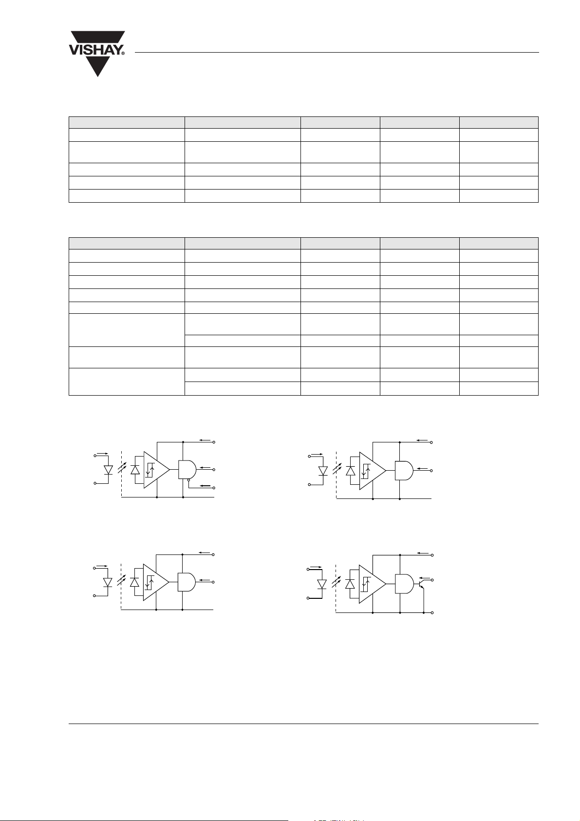
isfh6700_01
I
CC
V
I
F
(2)
(3)
Shield
SFH6700/19
I
F
(2)
(3)
Shield
SFH6701/11
CC
(8)
I
O
V
O
(7)
I
E
V
(6)
EN
GND
(5)
I
F
A
(2)
K
(3)
Shield
SFH6702/12
I
CC
V
CC
(8)
I
O
V
O
(7)
GND
(5)
I
F
A
(2)
K
(3)
Shield
SFH6705
I
CC
V
CC
(8)
I
O
V
O
(6)
GND
(5)
I
CC
V
CC
(8)
I
O
V
O
(6)
GND
(5)
Figure 1. Schematics
Document Number 83683
Rev. 1.5, 15-Apr-05
www.vishay.com
3
Page 4
SFH6700/ 01/ 02/ 05/ 11/ 12/ 19
Vishay Semiconductors
Recommended Operating Conditions
A 0.1 µF bypass capacitor connected between pins 5 and 8 must be used.
Parameter Test condition Par t Symbol Min Ty p. Max Unit
Supply voltage V
Enable voltage high SFH6700 V
SFH6719 V
Enable voltage low SFH6700 V
SFH6719 V
Forward input current I
Operating temperature T
Output pull-up resistor SFH6705 R
Fan Output R
(1)
We recommended using a 2.2 mA to permit at least 20 % CTR degradation guard band.
= 1.0 kΩ SFH6705 N 16 LS TTL
L
I
CC
EH
EH
EL
EL
Fon
Foff
A
L
Electrical Characteristics
- 40 °C ≤ T
Typical values: T
Minimum and maximum values are testing requirements. Typical values are characteristics of the device and are the result of engineering
evaluation. Typical values are for information only and are not part of the testing requirements.
≤ 85 °C; 4.5 V ≤ VCC ≤ 15 V; 1.6 mA ≤ I
amb
= 25 °C; VCC = 5.0 V; I
amb
Fon
≤ 5.0 mA; 2.0 ≤ VEH ≤ 15 V; 0 ≤ VEL ≤ 0.8 V; 0 mA ≤ I
Fon
= 3.0 mA unless otherwise specified
4.5 15 V
2.0 15 V
2.0 15 V
00.8V
00.8V
1.6
(1)
5.0 mA
0.1 mA
- 40 85 °C
350 4 kΩ
≤ 0.1 mA;
Foff
Loads
Input
Parameter Test condition Symbol Min Ty p. Max Unit
Forward voltage I
Input current hysteresis V
Reverse current V
Capacitance V
Thermal resistance R
= 5.0 mA V
F
I
= 5.0 mA, V
F
= 5.0 V, I
CC
= 3.0 V I
R
= 0 V, f = 1.0 MHz; C
R
HYS
= I
Fon-IFon
I
HYS
R
thja
F
F
1.6 1.75 V
1.8 V
0.1 mA
0.5 10 µA
O
60 pF
700 K/W
www.vishay.com
4
Document Number 83683
Rev. 1.5, 15-Apr-05
Page 5
SFH6700/ 01/ 02/ 05/ 11/ 12/ 19
Output
Parameter Test condition Symbol Min Ty p . Max Unit
Logic low output voltage I
Logic high output voltage
(except SFH6705)
Output leakage current
(V
OUT>VCC
) (except SFH6705)
Output leakage current
(SFH705 only)
Logic high enable voltage
(SFH6700/19 only)
Logic low enable voltage
(SFH6700/19 only)
Logic high enable current
(SFH6700/19 only)
Logic low enable current
(SFH6700/19 only)
High impedance state output
current (SFH6700/19 only)
Logic low supply current V
Logic high supply current V
Logic low short circuit output
2)
current
Logic high short circuit output
2)
current
Thermal resistance R
2)
Output short circuit time ≤ 10ms.
= 6.4 mA V
OL
I
= 2.6 mA, VOH = VCC-1.8 V 2.4 V
OH
= 5.5 V, VCC = 4.5 V,
V
O
I
= 5.0 mA
F
V
= 15 V, VCC = 4.5 V,
O
I
= 5.0 mA
F
V
= 5.5 V, VCC = 5.5 V,
O
= 5.0 mA
I
F
V
= 15 V, VCC = 15 V,
O
= 5.0 mA
I
F
= 2.7 V I
V
EN
= 5.5 V I
V
EN
V
= 15 V I
EN
V
= 0.4 V I
EN
= 0.4 V, VEN = 2.0 V,
V
O
= 5.0 mA
I
F
V
= 2.4 V, VEN = 2.0 V,
O
= 0 mA
I
F
V
= 5.5 V, VEN = 2.0 V,
O
= 0 mA
I
F
= 5.5 V, IF = 0 I
CC
V
= 15 V, IF = 0 I
CC
= 5.5 V, IF = 5.0 mA I
CC
V
= 15V, IF = 5.0 mA I
CC
VO = VCC = 5.5 V, IF = 0 I
= VCC = 15 V, IF = 0 I
V
O
VCC = 5.5 V, VO = 0 V,
= 5.0 mA
I
F
V
= 15 V, VO = 0 V,
CC
= 5.0 mA
I
F
I
OHH
I
OHH
I
OHH
I
OHH
V
V
I
OZL
I
OZH
I
OZH
I
OZH
CCL
CCL
CCH
CCH
OSL
OSL
I
OSL
I
OSL
EH
EH
EH
EL
OL
EH
EL
thja
Vishay Semiconductors
0.5 V
0.5 100 µA
1.0 500 µA
0.5 100 µA
1.0 500 µA
2.0 V
0.8 V
20 µA
100 µA
0.001 250 µA
- 320 - 50 µA
- 20 µA
20 µA
100 µA
0.001 500 µA
3.7 6.0 mA
4.1 6.5 mA
3.4 4.0 mA
3.7 5.0 mA
25 mA
40 mA
- 10 mA
- 25 mA
300 K/W
Coupler
Parameter Test condition Symbol Min Ty p . Max Unit
Capacitance (input-output) f = 1.0 MHz, pins 1-4 and 5-8
shorted together
Isolation resistance V
Document Number 83683
Rev. 1.5, 15-Apr-05
= 500 V, T
IO
V
= 500 V, T
IO
= 25 °C R
amb
= 100 °C R
amb
C
IO
IO
IO
10
10
12
11
0.6 pF
Ω
Ω
www.vishay.com
5
Page 6
SFH6700/ 01/ 02/ 05/ 11/ 12/ 19
Vishay Semiconductors
Switching Characteristics
0°C ≤ T
≤ I
Foff
Typical values: T
Propagation delay time to logic
low output level, SFH6700/01/
02/11/12/19
Output enable time to logic high
(SFH6700/19)
Output enable time to logic low
(SFH6700/19)
Output disable time from logic
low (SFH6700/19)
Output rise time 10 % to 90 % t
Output fall time 90 % to 10 % t
(3) A 0.1 µF bypass capacitor connected between pins 5 and 8 must be used
Typical values: T
Propagation delay time to logic
low output level
Output rise time 10 % to 90 % t
≤ 85 °C; 4.5 V ≤ VCC ≤ 15 V; 1.6 mA ≤ I
amb
≤ 0.1 mA
= 25 °C; VCC = 5.0 V; I
amb
Fon
≤ 5.0 mA; 2.0 ≤ VEH ≤ 15 V (SFH6700/19); 0 ≤ VEL ≤ 0.8 V (SFH6700/19); 0 mA
Fon
= 3.0 mA unless otherwise specified.
Parameter Test condition Symbol Min Ty p. Max Unit
Without peaking capacitor t
With peaking capacitor t
= 25 °C, VCC = 5.0 V; I
amb
= 3.0 mA; RL = 390 Ω unless otherwise specified
Fon
PHL
PHL
t
PLH
t
PLH
t
PZH
t
t
PZL
PLZ
r
f
Parameter Test condition Par t Symbol Min Ty p. Max Unit
Without peaking capacitor SFH6705 t
With peaking capacitor SFH6705 t
Without peaking capacitor SFH6705 t
With peaking capacitor SFH6705 t
90 % to 10 % t
PHL
PHL
PLH
PLH
(3)
120 ns
115 300 ns
125 ns
90 300 ns
20 ns
25 ns
50 ns
40 ns
10 ns
(3)
115 ns
105 300 ns
125 ns
90 300 ns
r
r
25 ns
4ns
www.vishay.com
6
Document Number 83683
Rev. 1.5, 15-Apr-05
Page 7

SFH6700/ 01/ 02/ 05/ 11/ 12/ 19
isfh6700_03
VF- Forward Voltage
I
F
- Forward Current - mA
0.010
0.100
1.000
10.000
1.3
1.4 1.5 1.6 1.7
Vishay Semiconductors
Common Mode Transient Immunity
T
= 25 °C, VCC = 5.0 V
amb
Parameter Test condition Par t Symbol Min Ty p. Max Unit
Logic High Common Mode
Transient Immunity
Logic Low Common Mode
Transient Immunity
(4)
CMH is the maximum slew rate of a common mode voltage VCM at which the output voltage remains at logic high level (VO > 2.0 V)
is the maximum slew rate of a common mode voltage VCM at which the output voltage remains at logic high level (VO < 0.8 V)
CM
L
(4)
| = 50 V, IF = 1.6 mA SFH6700
|V
CM
| = 400 V, IF = 1.6 mA SFH6711
|V
CM
| = 50V, IF = 0 mA SFH6700
|V
CM
| = 50 V, IF = 0 mA SFH6701
|V
CM
| = 400 V, IF = 0 mA SFH6711
|V
CM
SFH6701
SFH6702
SFH6705
SFH6712
SFH6719
SFH6702
SFH6705
SFH6712
SFH6719
|CM
|CM
|CM
|CM
|CM
|CM
|CM
|CM
|CM
|CM
|CM
|CM
|CM
|CM
(4)
1000 V/µs
|
H
(4)
1000 V/µs
|
H
(4)
1000 V/µs
|
H
(4)
1000 V/µs
|
H
(4)
2500 V/µs
|
H
(4)
2500 V/µs
|
H
(4)
2500 V/µs
|
H
(4)
1000 V/µs
|
L
(4)
1000 V/µs
|
L
(4)
1000 V/µs
|
L
(4)
1000 V/µs
|
L
(4)
2500 V/µs
|
L
(4)
2500 V/µs
|
L
(4)
2500 V/µs
|
L
Typical Characteristics (Tamb = 25 °C unless otherwise specified)
150
120
100
75
50
25
- Power dissipation - mW
tot
0
P
–60 100806040200–20–40
isfh6700_02
Figure 2. Permissible Total Power Dissipation vs. Temperature
Detector
Emitter
TA- Temperature - °C
Figure 3. Typical Input Diode Forward Current vs. Forward Voltage
Document Number 83683
Rev. 1.5, 15-Apr-05
www.vishay.com
7
Page 8

SFH6700/ 01/ 02/ 05/ 11/ 12/ 19
isfh6700_07
-60 -40 -20 0 20 40 60 80 100
3.2
3.4
3.6
3.8
4.0
4.2
TA- Temperature - °C
I
CC
- Supply Curent - mA
I
CCL@VCC
=15V
I
CCH@VCC
=15V&
I
CCL@VCC
= 5.5 V
I
CCH@VCC
= 5.5 V
isfh6700_08
-20 0 20 40 60 80 100
TA- Temperature - °C
400
500
600
700
800
900
1000
1100
-60 -40
I
OHH
- Output Leakage
Current - nA
VCC=VO=15V
VCC=VO= 5.5 V
isfh6700_09
-20 0 20406080100
TA- Temperature - °C
20
23
25
28
30
33
35
38
40
-60 -40
I
OL
- Low Level Output
Current - mA
VCC=5V
IF=0mA
VOL= 0.6 V
VOL= 0.4 V
VOL= 0.8 V
Vishay Semiconductors
1.75
1.70
IF=5mA
1.65
1.60
1.55
1.50
- Forward Voltage - V
F
V
1.45
-60 -40 -20 0 20 40 60 80 100
TA - Temperature - °C
isfh6700_04
Figure 4. Typical Forward Input Voltage vs. Temperature
5
VCC= 4.5 V
4
3
2
1
- Output Voltage - V
O
V
IOL= 6.4 mA
0
0.0 0.1 0.2 0.3 0.4 0.5 0.6 0.7 0.8 0.9 1.0
IF-Input Current - mA
IOH=–2.6mA
Figure 7. Typical Supply Current vs. Temperature
isfh6700_05
Figure 5. Typical Output Voltage vs. Forward Input Current (except
SFH6705)
6
VCC=5V
5
4
3
RL=1k-4kΩ
2
- Output Voltage - V
1
O
V
0
RL= 390 Ω
0.0 0.2 0.4 0.6 0.8 1.0
IF- Forward Input Current - mA
isfh6700_06
Figure 6. Typical Output Forward Voltage vs. Forward Input
www.vishay.com
8
Current (only SFH6705)
Figure 8. Typical Output Leakage Current vs. Temperature
Figure 9. Typical Low Level Output Current vs. Temperature
Document Number 83683
Rev. 1.5, 15-Apr-05
Page 9

- Low Level Output
isfh6700_24
-60 -40 -20 0 20 40 60 80 100
t
PLH
- Propagation Delay - ns
TA- Temperature - °C
70
90
110
130
150
VCC=5V
C = 15 pF (without peaking capacitor)
IF=3mA
IF=5mA
IF= 1.6 mA
isfh6700_14
-60 -40 -20 0 20 40 60 80 100
t
PHL
- Propagation Delay - ns
TA- Temperature - °C
60
80
100
120
140
160
180
VCC=5V
C1 = 15 pF (without peaking capacitor)
IF=5mA
IF=3mA
IF= 1.6 mA
isfh6700_15
-60 -40 -20 0 20 40 60 80 100
t
PLH
- Propagation Delay - ns
TA- Temperature - °C
50
60
70
80
90
100
VCC=5V
C1 = 120 pF (without peaking capacitor)
IF=1.6,3and5mA
OL
V
isfh6700_10
0.30
VCC=5V
IF=0mA
0.25
IO=16mA
0.20
IO= 12.8 mA
0.15
Voltage - V
IO= 9.6 mA
0.10
IO= 6.4 mA
0.05
-60 -40 -20 0 20 40 60 80 100
TA- Temperature - °C
SFH6700/ 01/ 02/ 05/ 11/ 12/ 19
Vishay Semiconductors
Figure 10. Typical Low Level Output Voltage vs. Temperature
0
-1
VOH= 2.7 V
-2
-3
-4
Current - mA
- High Level Output
OH
I
-5
-6
-7
-8
VOH= 2.4 V
-60 -40 -20 0 20 40 60 80 100
TA- Temperature - °C
isfh6700_11
VCC= 4.5 V
IF=5mA
Figure 11. Typical High Level Output Current vs. Temperature
(except SFH6705
60
54
VCC=5V
48
IF=3mA
42
36
30
t
R
24
18
-Rise, Fall Time - ns
12
F
,t
R
t
t
F
6
0
-60 -40 -20 0 20 40 60 80 100
TA- Temperature - °C
Figure 13. Typical Propagation Delay to Logic High vs.
Temperature (except SFH6705)
Figure 14. Typical Propagation Delay to Logic LOw vs.
Temperature (except SFH6705)
isfh6700_12
Figure 12. Typical Rise, Fall Time vs. Temperature (except
Document Number 83683
Rev. 1.5, 15-Apr-05
SFH6705)
Figure 15. Typical Propagation Delays to Logic High vs.
Temperature (except SFH6705)
www.vishay.com
9
Page 10

SFH6700/ 01/ 02/ 05/ 11/ 12/ 19
isfh6700_19
-60 -40 -20 0 20 40 60 80 100
t
PLH
- Propagation Delay - ns
TA- Temperature - °C
30
40
50
60
70
80
VCC=5V
C1 = 120 pF (without peaking capacitor)
IF=1.6,3and5mA
isfh6700_20
60
80
100
120
140
160
180
-60 -40 -20 0 20 40 60 80 100
VCC=15V
C1 = 120 pf (Peaking Capacitor is used)
IF=5mA
TA- Temperature - °C
t
PHL
-Propagation Delay - ns
IF=3mA
IF= 1.6 mA
isfh6700_21
t
p
- Enable Propagation
Delay - ns
TA- Temperature - °C
0
10
20
30
40
50
60
70
80
-60 -40 -20 0 20 40 60 80 100
CL=15pF
VCC=15V
VCC= 4.5 –15 V
t
PZL
t
PLZ
VCC= 4.5 V
Vishay Semiconductors
170
VCC=5V
150
C1 = 120 pF (without peaking capacitor)
130
110
IF=5mA
90
PHL
70
50
IF= 1.6 mA
- Propagation Delay - ns
t
-60 -40 -20 0 20 40 60 80 100
TA- Temperature - °C
isfh6700_16
IF=3mA
Figure 16. Typical Propagation Delay to Logic Low vs.
Temperature
VCC=15V
C1 = 15 pF (without
peaking capacitor)
90
80
70
- Propagation Delay - ns
60
PLH
t
50
-60 -40 -20 0 20 40 60 80 100
TA- Temperature - °C
isfh6700_17
IF= 1.6 mA
IF=3mA
IF=5mA
Figure 17. Typical Propagation Delays to Logic High vs.
Temperature
170
VCC=5V
C1 = 15 pF (without
150
peaking capacitor)
130
110
90
- Propagation Delay - ns
70
PHL
t
50
-60 -40 -20 0 20 40 60 80 100
IF=5mA
IF= 1.6 mA
TA- Temperature - °C
IF=3mA
Figure 19. Typical Propagation Delays to Logic High vs.
Temperature
Figure 20. Typical propagation delays to Logic Low vs.
temperature (except SFH6705)
isfh6700_18
Figure 18. Typical Propagation Delays to Logic Low
www.vishay.com
10
vs.Temperature
Figure 21. Typical Logic Low Enable Propagation Delays vs.
Temperature (only SFH6700/11)
Document Number 83683
Rev. 1.5, 15-Apr-05
Page 11

80
isfh6700_25
-60 -40 -20 0 20 40 60 80 100
TA- Temperature - °C
t
PHL
- Propagation Delay - ns
70
80
90
100
110
120
130
140
ˇ
VCC=5V
RL= 350 - 4 kΩ
IF=5mA
IF=3mA
IF= 1.6 mA
isfh6700_26
-25
0
25
50
-60 -40 -20 0 20 40 60 80 100
250
225
tR@RL=4kΩ
VCC=5V
200
t
R
,t
F
-Rise, Fall Time - ns
TA- Temperature - °C
tR@RL=1kΩ
tR@RL= 350 kΩ
tF@RL= 350-4 kΩ
CL=15pF
70
60
50
40
30
Delay - ns
20
10
tP - Enable Propagation
0
-60 -40 -20 0 20 40 60 80 100
isfh6700_22
VCC= 4.5 V
VCC= 4.5 V –15 V
VCC=15V
TA- Temperature - °C
SFH6700/ 01/ 02/ 05/ 11/ 12/ 19
Vishay Semiconductors
t
PHZ
t
PZH
t
PHZ
Figure 22. Typical Logic High Enable Propagation Delays vs.
Temperature (only SFH6700/11)
- Propagation Delay - ns
P
t
isfh6700_23
250
200
150
100
50
1357911
t
PLH@RL
=1kΩ
ˇ
t
PHL@RL
IF- Pulse Input Current - mA
VCC=5V
t
PLH@RL
t
PLH@RL
ˇ
=4kΩ
ˇ
= 350 –4 kΩ
ˇ
=35kΩ
Figure 23. Typical Propagation Delays vs. Pulse Input Current
(only SFH6705)
220
VCC=5V
IF=3mA
200
180
ˇ
160
140
120
- Propagation Delay - ns
100
80
PLH
t
-60 -40 -20 0 20 40 60 80 100
RL=4kΩ
RL=1kΩ
ˇ
RL= 350 kΩ
ˇ
TA- Temperature - °C
Figure 25. Typical Propagation Delays to Low Level vs.
Temperature ( only SFH6705)
Figure 26. Typical Rise, Fall Time vs. Temperature (only
SFH6705)
isfh6700_24
Figure 24. Typical Propagation Delays to High Level vs.
Document Number 83683
Rev. 1.5, 15-Apr-05
Temperature (only SFH6705)
www.vishay.com
11
Page 12

SFH6700/ 01/ 02/ 05/ 11/ 12/ 19
Vishay Semiconductors
isfh6700_27
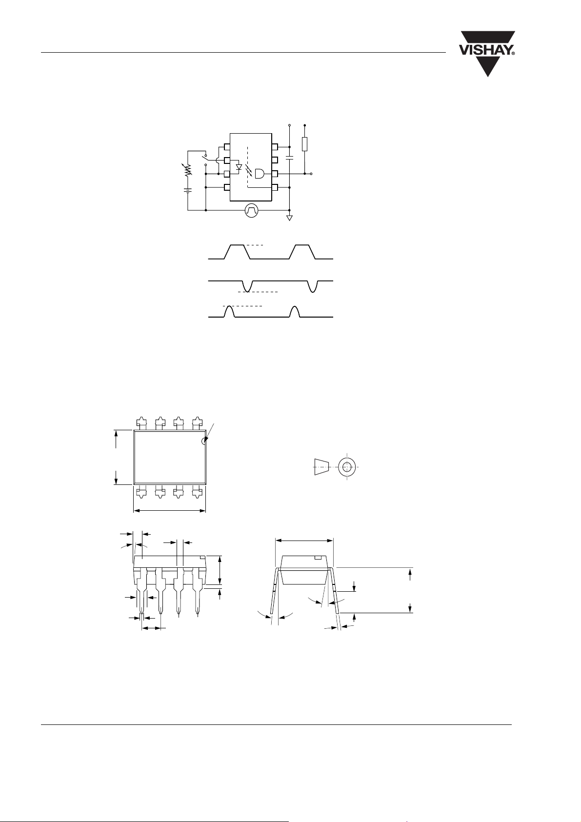
Pulse generator
tr,tf=5ns
f = 100 kHz
10% Duty cycle
Input I
F
Monitoring
Node
The Probe and Jig Capacitances are included in C1 and C2
R1
2.15 kOhm
IF(ON)
1.6 mA
Input I
F
Output V
O
R1
C1 = 120 pF
1
I
F
2
3
4
1.1 kOhm
3mA
t
PLH
681 Ohm
5mA
V
Out*
Gnd
CC
En*
Figure 27. Test Circuit for t
V
CC
R3 = 619 Ohm
Output Vo
8
7
6
5
Monitoring
Node
0.1 µF
Bypass
C2 = 15 pF R2 = 5 kOhm
All diodes are 1N916 or 1N3064
* SFH6701/02/11/12 without V
* SFH6702/12 Pin 6 V
I
Fon
50%
0mA
V
OH
1.3 V
t
PHL
, t
PHL
, tr and t
PLH
D1
OUT
I
Fon
V
5V
OL
D2
D3
D4
EN
and Pin 7 n.c.
f
isfh6700_28
Pulse generator
tr,tf=5ns
Zo = 50 Ohm
Input I
F
Monitoring
Node
The Probe and Jig Capacitances are included in C1 and C2
R1
2.15 kOhm
IF(ON)
1.6 mA
Input I
F
Output V
O
R1
1
I
F
2
3
4
C1 = 120 pF
1.1 kOhm
3mA
t
PLH
681 Ohm
5mA
V
V
CC
n.c.
OUT
Gnd
Figure 28. Test Circuit for t
8
7
6
5
PLH
V
5V
CC
R
L
0.1 µF
Bypass
C2 = 15 pF
t
PHL
, t
, tr and - SFH6705
PHL
I
Fon
50%
0mA
V
1.3 V
OH
Output V
Monitoring
Node
I
Fon
V
OL
O
www.vishay.com
12
Document Number 83683
Rev. 1.5, 15-Apr-05
Page 13

SFH6700/ 01/ 02/ 05/ 11/ 12/ 19
Pulse generator
ZO=50Ohm
tr,tf=5ns
I
F
Input V
C
Monitoring
Node
C1 = 15 pF including Probe and Jig Capacitances
1
2
3
4
V
V
CC
8
Out
7
6
En
5
Gnd
All diodes are 1N916 or 1N3064
CC
Output V
Monitoring
Node
5kOhm
0.1µF
Bypass
C1
O
619 Ohm
D1
Vishay Semiconductors
5V
S1
D2
D3
D4
S2
isfh6700_29
Input V
EN
Output V
Output V
O
S1 closed
S2 open
S1 open
S2 closed
O
t
PZL
t
PZH
1.3 V
1.3 V
0V
Figure 29. Test Circuit for t
1
A
2
R
* SFH6701/02/11/12 without V
* SFH6702/12 Pin 6 V
B
3
4
Pulse Generator
OUT
PHZ
V
Out*
En*
Gnd
+
–
VCM
EN
and Pin 7 n.c.
3.0 V
1.3 V
0V
S1 and S2 closed
0.5 V
V
OL
t
PLZ
0.5 V
V
OH
ca. 1.5 V
S1andS2closed
t
PHZ
, t
, t
PZH
8
cc
7
6
5
and t
PLZ
V
CC
Output V
Monitoring
Node
0.1µF
Bypass
-SFH6700/19
PZL
O
isfh6700_30
Figure 30. Test Circuit for Common Mode Transient Immunity and Typical Waveforms-SFH6700/01/02/11/12/19
Document Number 83683
Rev. 1.5, 15-Apr-05
VCM
Output V
400V/50V
0V
V
OH
O
V
OL
Switch at A: IF= 1.6 mA
VO(min)
VO(max)
Switch at B: IF=0mA
www.vishay.com
13
Page 14
SFH6700/ 01/ 02/ 05/ 11/ 12/ 19
Vishay Semiconductors
V
5V
CC
R
1
A
2
B
3
4
Pulse Generator
8
7
n.c.
6
Out
5
Gnd
+
–
VCM
0.1µF
Bypass
R
L
Output V
Monitoring
Node
O
VCM
0V
V
OH
Output V
O
V
isfh6700_31
OL
Switch at B: IF=0mA
Figure 31. Test Circuit for Common Mode Transient Immunity and Typical Waveforms-SFH6705
Package Dimensions in Inches (mm)
pin one ID
i178006
.255 (6.48)
.268 (6.81)
.030 (0.76)
.045 (1.14)
4° typ.
.050 (1.27)
.018 (.46)
.022 (.56)
4
3
5
6
.379 (9.63)
.390 (9.91)
1
2
78
.031 (0.79)
.130 (3.30)
.150 (3.81)
.020 (.51 )
.035 (.89 )
.100 (2.54) typ.
50 V
Switch at A: IF= 1.6 mA
VO(min)
VO(max)
.300 (7.62)
3°–9°
.008 (.20)
.012 (.30)
typ.
10°
ISO Method A
.110 (2.79)
.130 (3.30)
.230(5.84)
.250(6.35)
www.vishay.com
14
Document Number 83683
Rev. 1.5, 15-Apr-05
Page 15

SFH6700/ 01/ 02/ 05/ 11/ 12/ 19
Vishay Semiconductors
Option 6
.407 (10.36)
.391 (9.96)
.307 (7.8)
.291 (7.4)
.014 (0.35)
.010 (0.25)
.400 (10.16)
.430 (10.92)
.028 (0.7)
MIN.
Option 7
.300 (7.62)
TYP.
.315 (8.0)
MIN.
.331 (8.4)
MIN.
.406 (10.3)
MAX.
.180 (4.6)
.160 (4.1)
.0040 (.102)
.0098 (.249)
Option 9
.375 (9.53)
.395 (10.03)
.300 (7.62)
ref.
.020 (.51)
.040 (1.02)
.315 (8.00)
min.
.012 (.30) typ.
15° max.
18450
Document Number 83683
Rev. 1.5, 15-Apr-05
www.vishay.com
15
Page 16

SFH6700/ 01/ 02/ 05/ 11/ 12/ 19
Vishay Semiconductors
Ozone Depleting Substances Policy Statement
It is the policy of Vishay Semiconductor GmbH to
1. Meet all present and future national and international statutory requirements.
2. Regularly and continuously improve the performance of our products, processes, distribution and operating
systems with respect to their impact on the health and safety of our employees and the public, as well as
their impact on the environment.
It is particular concern to control or eliminate releases of those substances into the atmosphere which are
known as ozone depleting substances (ODSs).
The Montreal Protocol (1987) and its London Amendments (1990) intend to severely restrict the use of ODSs
and forbid their use within the next ten years. Various national and international initiatives are pressing for an
earlier ban on these substances.
Vishay Semiconductor GmbH has been able to use its policy of continuous improvements to eliminate the use
of ODSs listed in the following documents.
1. Annex A, B and list of transitional substances of the Montreal Protocol and the London Amendments
respectively
2. Class I and II ozone depleting substances in the Clean Air Act Amendments of 1990 by the Environmental
Protection Agency (EPA) in the USA
3. Council Decision 88/540/EEC and 91/690/EEC Annex A, B and C (transitional substances) respectively.
Vishay Semiconductor GmbH can certify that our semiconductors are not manufactured with ozone depleting
substances and do not contain such substances.
We reserve the right to make changes to improve technical design
and may do so without further notice.
Parameters can vary in different applications. All operating parameters must be validated for each
customer application by the customer. Should the buyer use Vishay Semiconductors products for any
unintended or unauthorized application, the buyer shall indemnify Vishay Semiconductors against all
claims, costs, damages, and expenses, arising out of, directly or indirectly, any claim of personal
damage, injury or death associated with such unintended or unauthorized use.
Vishay Semiconductor GmbH, P.O.B. 3535, D-74025 Heilbronn, Germany
www.vishay.com
16
Document Number 83683
Rev. 1.5, 15-Apr-05
Page 17

Legal Disclaimer Notice
Vishay
Document Number: 91000 www.vishay.com
Revision: 08-Apr-05 1
Notice
Specifications of the products displayed herein are subject to change without notice. Vishay Intertechnology, Inc.,
or anyone on its behalf, assumes no responsibility or liability for any errors or inaccuracies.
Information contained herein is intended to provide a product description only. No license, express or implied, by
estoppel or otherwise, to any intellectual property rights is granted by this document. Except as provided in Vishay's
terms and conditions of sale for such products, Vishay assumes no liability whatsoever, and disclaims any express
or implied warranty, relating to sale and/or use of Vishay products including liability or warranties relating to fitness
for a particular purpose, merchantability, or infringement of any patent, copyright, or other intellectual property right.
The products shown herein are not designed for use in medical, life-saving, or life-sustaining applications.
Customers using or selling these products for use in such applications do so at their own risk and agree to fully
indemnify Vishay for any damages resulting from such improper use or sale.
 Loading...