

Page 1
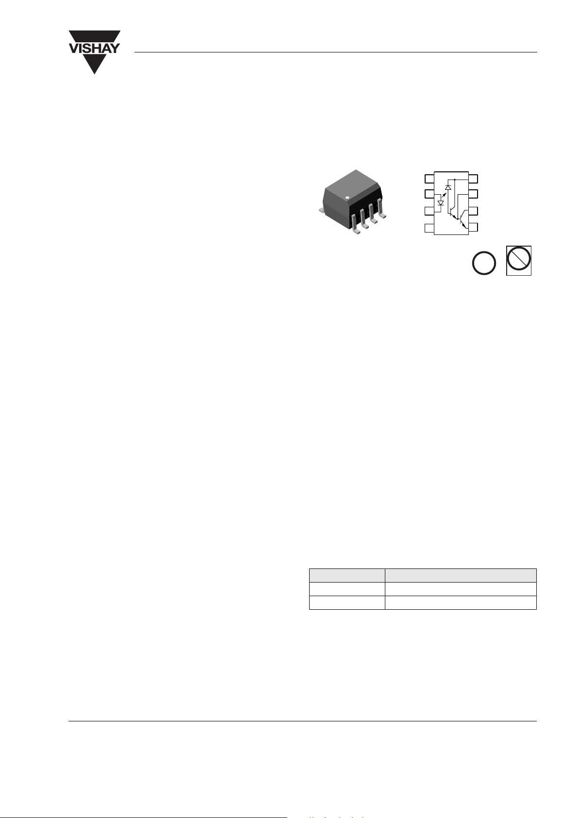
SFH6318T/ SFH6319T
i179070
1
2
3
4
8
7
6
5
V
CC
NC
A
C
NC
V
0
V
B
GND
Vishay Semiconductors
High Speed Optocoupler, 100 kBd, Low Input Current, High Gain
Features
• Industry Standard SOIC-8 Surface Mountable
Package
• High Current Transfer Ratio, 800 %
• Low Input Current, 0.5 mA
• High Output Current, 60 mA
• Isolation Test Voltage, 3000 V
• TTL Compatible Output, VOL = 0.1 V
• Adjustable Bandwidth-Access to Base
• Lead-free component
RMS
e3
Pb
Pb-free
• Component in accordance to RoHS 2002/95/EC
and WEEE 2002/96/EC
Agency Approvals
• UL1577, File No. E52744 System Code H or J,
Double Protection
• DIN EN 60747-5-2 (VDE0884)
DIN EN 60747-5-5 pending
Available with Option 1
• CSA 93751
Applications
Logic Ground Isolation -TTL/TTL, TTL/CMOS,
CMOS/CMOS, CMOS/TTL
EIA RS 232C Line Receiver
Low Input Current Line Receiver Long Lines, Party
Lines
Telephone Ring Detector
117 VAC Line Voltage Status Indication - Low Input
Power Dissipation
Low Power Systems - Ground Isolation
Description
Very high current ratio together with 3000 V
tion are achieved by coupling an LED with an integrated high gain photo detector in a SOIC-8 package.
Separate pins for the photo diode and output stage
RMS
isola-
enable TTL compatible saturation voltages with high
speed operation. Photodarlington operation is
achieved by tying the V
and VO terminals together.
CC
Access to the base terminal allows adjustment to the
gain bandwidth.
The SFH6318T is ideal for TTL applications since the
300 % minimum current transfer ratio with an LED
current of 1.6 mA enables operation with one unit
load-in and one unit load-out with a 2.2 kΩ pull-up
resistor.
The SFH6319T is best suited for low power logic
applications involving CMOS and low power TTL. A
400 % current transfer ratio with only 0.5 mA of LED
current is guaranteed from 0 °C to 70 °C.
Caution:
Due to the small geometries of this device, it should
be handled with Electrostatic Discharge (ESD) precautions. Proper grounding would prevent damage
further and/or degradation which may be induced by
ESD.
Order Information
Part Remarks
SFH6318T CTR 1600 (300 - 2600) %, SOIC-8
SFH6319T CTR 2000 (400 - 3500) %, SOIC-8
For additional information on the available options refer to
Option Information.
Note Product available only on tape and reel
Document Number 83678
Rev. 1.4, 26-Oct-04
www.vishay.com
1
Page 2
SFH6318T/ SFH6319T
Vishay Semiconductors
Absolute Maximum Ratings
T
= 25 °C, unless otherwise specified
amb
Stresses in excess of the absolute Maximum Ratings can cause permanent damage to the device. Functional operation of the device is
not implied at these or any other conditions in excess of those given in the operational sections of this document. Exposure to absolute
Maximum Rating for extended periods of the time can adversely affect reliability.
Input
Parameter Test condition Par t Symbol Val ue Unit
Reverse input voltage V
Supply and output voltage V
(pin 8-5), VO (pin 6-5) SFH6318T VCC, V
CC
SFH6319T V
Input power dissipation P
CC
R
, V
diss
O
O
Derate linearly above 50 °C
Free air temperature 0.7 mW/°C
Average input current I
Peak input current 50 % duty cycle-1.0 ms pulse
width
Peak transient input current t
≤ 1.0 µs, 300 pps I
p
F(AVG)
I
FRM
FSM
3.0 V
- 0.5 to 7.0 V
- 0.5 to 18 V
35 mW
20 mA
40 mA
1.0 A
Output
Parameter Test condition Symbol Val ue Unit
Output current (pin 6) I
Emitter-base reverse current
O
60 mA
0.5 V
(pin 5-7)
Output power dissipation P
diss
150 mW
Derate linearly from 25 °C 2.0 mW/°C
Coupler
Parameter Test condition Symbol Val ue Unit
Storage temperature T
Lead soldering temperature t = 10 s T
Junction temperature T
Ambient temperature range T
Isolation test voltage between
V
stg
sld
j
amb
ISO
emitter and detector (refer to
climate DIN 40046, part 2, Nov.
74)
Pollution degree (DIN VDE
0110)
Creepage distance ≥ 4.0 mm
Clearance ≥ 4.0 mm
Comparative tracking index per
DIN IEC 112/VDE 0303, part 1
Isolation resistance V
= 500 V, T
IO
V
= 500 V, T
IO
= 25 °C R
amb
= 100 °C R
amb
IO
IO
- 55 to + 125 °C
260 °C
100 °C
- 55 to + 100 °C
3000 V
RMS
2
175
12
≥ 10
11
≥ 10
Ω
Ω
www.vishay.com
2
Document Number 83678
Rev. 1.4, 26-Oct-04
Page 3
SFH6318T/ SFH6319T
Vishay Semiconductors
Electrical Characteristics
T
= 25 °C, unless otherwise specified
amb
Minimum and maximum values are testing requirements. Typical values are characteristics of the device and are the result of engineering
evaluation. Typical values are for information only and are not part of the testing requirements.
Input
T
= 0 °C to 70 °C. Typical values are specified at T
amb
Parameter Test condition Part Symbol Min Ty p. Max Unit
Input forward voltage I
Temperature coefficient, forward
= 1.6 mA V
F
I
= 1.6 mA ∆VF/
F
voltage
Output
T
= 0 °C to 70 °C. Typical values are specified at T
amb
Parameter Test condition Symbol Min Ty p. Max Unit
Logic low output voltage,
see note 2
Logic high output current,
see note 2
Logic low supply current,
see note 2
Logic high supply current,
see note 2
= 1.6 mA, IO = 4.8 mA,
I
F
= 4.5 V
V
CC
I
= 1.6 mA, IO = 8.0 mA,
F
= 4.5 V
V
CC
I
= 5.0 mA, IO = 15 mA,
F
= 4.5 V
V
CC
I
= 12 mA, IO = 24 mA,
F
= 4.5 V
V
CC
I
= 0 mA, VO = VCC = 7.0 V I
F
= 0 mA, VO = VCC = 18 V I
I
F
I
= 1.6 mA, VO = OPEN,
F
= 18 V
V
CC
I
= 0 mA, VO = OPEN,
F
V
= 18 V
CC
amb
amb
= 25 °C.
= 25 °C.
V
V
V
V
I
CCL
I
CCH
OL
OL
OL
OL
IO
IO
∆T
F
amb
1.4 1.7 V
- 1.8 mV/°C
0.1 0.4 V
0.1 0.4 V
0.15 0.4 V
0.25 0.4 V
0.1 250 µA
0.05 100 µA
0.2 1.5 mA
0.01 10 µA
Coupler
T
= 0 °C to 70 °C. Typical values are specified at T
amb
amb
= 25 °C.
Parameter Test condition Symbol Min Ty p. Max Unit
Capacitance (input-output) (see
f = 1.0 MHz C
IO
0.6 pF
note 3)
Input capacitance f = 1.0 MHz, V
Resistance (input-output),
see note 3
V
= 500 VDC, T
IO
= 500 VDC, T
V
IO
= 0 C
F
= 25 °C R
amb
= 100 °C R
amb
IN
IO
IO
25 pF
12
10
11
10
Current Transfer Ratio
T
= 0 °C to 70 °C. Typical values are specified at T
amb
Para me ter Test condition Part Symbol Min Ty p. Max Unit
Current Transfer
IF = 1.6 mA, VO = 0.4 V, VCC = 4.5 V SFH6318T CTR 300 1600 2600 %
Ratio
See notes 1 and 2
= 0.5 mA, VO = 0.4 V, VCC = 4.5 V SFH6319T CTR 400 2000 3500 %
I
F
I
= 1.6 mA, VO = 0.4 V, VCC = 4.5 V SFH6319T CTR 500 1600 2600 %
F
Document Number 83678
Rev. 1.4, 26-Oct-04
amb
= 25 °C.
Ω
Ω
www.vishay.com
3
Page 4

SFH6318T/ SFH6319T
Vishay Semiconductors
Switching Characteristics
T
= 25 °C
amb
Parameter Test condition Part Symbol Min Ty p . Max Unit
Propagation delay time to logic
= 1.6 mA, RL = 2.2 kΩ SFH6318T t
I
F
PHL
low at output
Propagation delay time to logic
low at output, see notes 2 and 4
Propagation delay time to logic
low at output
Propagation delay time to logic
= 0.5 mA, RL = 4.7 kΩ SFH6319T t
I
F
= 12 mA, RL = 270 Ω SFH6319T t
I
F
= 1.6 mA, RL = 2.2 kΩ SFH6318T t
I
F
PHL
PHL
PLH
high at output
Propagation delay time to logic
high at output, see notes 2 and 4
Propagation delay time to logic
high at output
= 0.5 mA, RL = 4.7 kΩ SFH6319T t
I
F
= 12 mA, RL = 270 Ω SFH6319T t
I
F
PLH
PLH
Common Mode Transient Immunity
Parameter Test condition Symbol Min Typ . Max Unit
I
Common mode transient
immunity at logic high level
output, see notes 5 and 6
Common mode transient
immunity at logic low level
output, see notes 5 and 6
= 0 mA, RL = 2.2 kΩ,
F
= 10 V
V
CM
I
= 1.6 mA, RL = 2.2 kΩ,
F
V
CM
= 10 V
P-P
P-P
1. DC current transfer ratio is defined as the ratio of output collector current, IO, to the forward LED input current, IF times 100 %
2. Pin 7 open.
3. Device considered a two-terminal device: pins 1, 2, 3 and 4 shorted together and pins 5, 6, 7 and 8 shorted together.
4. Using a resistor between pin 5 and 7 will decrease gain and delay time.
5. Common mode transient immunity in logic high level is the maximum tolerable (positive) dV
mode pulse, V
level is the maximum tolerable (negative) dV
will remain in a logic low state (i.e.V
, to assure that the output will remain in a logic high state (i.e. VO > 2.0 V) common mode transient immunity in logic low
CM
< 0.8 V).
O
/dt on the trailing edge of the common mode pulse signal, VCM, to assure that the output
cm
6. In applications where dv/dt may exceed 50,000 V/µs (such as state discharge) a series resistor, R
from destructively high surge currents. The recommended value is Refer to Figure 2.
R
≅ [(IV)/0.15 IF (mA)] kΩ.
CC
I CMH I1K V/µs
I CML I1K V/µs
/dt on the leading edge of the common
cm
2.0 10 µs
6.0 25 µs
0.6 1.0 µs
2.0 35 µs
4.0 60 µs
1.5 7.0 µs
should be included to protect I
CC
C
10% Duty Cycl
1/f<100
µs
Pulse
Generator
ZO=50Ω
tr=5ns
IF= Monitor
isfh6318t_01
www.vishay.com
4
I
F
0
R
µ
L
F
+5 V
V
O
CL=15pF
V
O
(Saturated
Response)
t
PHL
V
O
(Non-Saturated
Response)
90%
10%
1.5V
t
f
t
PLH
10%
90%
1.5V
5V
V
OL
5V
t
r
1
I
F
2
3
4
R
m
8
7
6
5
0.1
Figure 1. Switching Test Circuit
Document Number 83678
Rev. 1.4, 26-Oct-04
Page 5

RCC(see Note 6)
CM
8
7
6
5
220 Ω
0.1 µF
B
V
CC
isfh6318t_02
1
I
F
2
A
3
4
V
+–
Pulse Generator
Figure 2. Test Circuit for Transient Immunity and Typical Waveforms
Package Dimensions in Inches (mm)
SFH6318T/ SFH6319T
Vishay Semiconductors
+5 V
R
L
V
O
V
CM
10%
0V
V
O
Switch at A: IF=0mA
V
O
Switch at B: IF= 1.6 mA
90%
t
r
tf+tf=16 ns
90%
10%
t
f
5V
V
OL
.240
(6.10)
ISO Method A
i178003
.120± .005
(3.05± .13)
Pin One ID
.004 (.10)
.008 (.20)
.192± .005
(4.88± .13)
.050 (1.27)
.021 (.53)
typ.
.154± .005
C
L
(3.91± .13)
.016 (.41)
.050 (1.27)
.015± .002
(.38± .05)
.008 (.20)
.020± .004
(.51± .10)
2 plcs.
R .010 (.13)
.170 (4.32)
.260 (6.6)
40°
5° max.
R.010
(.25) max.
.014 (.36)
.036 (.91)
.045 (1.14)
7°
.058± .005
(1.49± .13)
.125± .005
(3.18± .13)
Lead
Coplanarity
±.0015 (.04)
max.
Document Number 83678
Rev. 1.4, 26-Oct-04
www.vishay.com
5
Page 6

SFH6318T/ SFH6319T
Vishay Semiconductors
Ozone Depleting Substances Policy Statement
It is the policy of Vishay Semiconductor GmbH to
1. Meet all present and future national and international statutory requirements.
2. Regularly and continuously improve the performance of our products, processes, distribution and
operatingsystems with respect to their impact on the health and safety of our employees and the public, as
well as their impact on the environment.
It is particular concern to control or eliminate releases of those substances into the atmosphere which are
known as ozone depleting substances (ODSs).
The Montreal Protocol (1987) and its London Amendments (1990) intend to severely restrict the use of ODSs
and forbid their use within the next ten years. Various national and international initiatives are pressing for an
earlier ban on these substances.
Vishay Semiconductor GmbH has been able to use its policy of continuous improvements to eliminate the use
of ODSs listed in the following documents.
1. Annex A, B and list of transitional substances of the Montreal Protocol and the London Amendments
respectively
2. Class I and II ozone depleting substances in the Clean Air Act Amendments of 1990 by the Environmental
Protection Agency (EPA) in the USA
3. Council Decision 88/540/EEC and 91/690/EEC Annex A, B and C (transitional substances) respectively.
Vishay Semiconductor GmbH can certify that our semiconductors are not manufactured with ozone depleting
substances and do not contain such substances.
We reserve the right to make changes to improve technical design
and may do so without further notice.
Parameters can vary in different applications. All operating parameters must be validated for each
customer application by the customer. Should the buyer use Vishay Semiconductors products for any
unintended or unauthorized application, the buyer shall indemnify Vishay Semiconductors against all
claims, costs, damages, and expenses, arising out of, directly or indirectly, any claim of personal
damage, injury or death associated with such unintended or unauthorized use.
Vishay Semiconductor GmbH, P.O.B. 3535, D-74025 Heilbronn, Germany
Telephone: 49 (0)7131 67 2831, Fax number: 49 (0)7131 67 2423
www.vishay.com
6
Document Number 83678
Rev. 1.4, 26-Oct-04
Page 7

Legal Disclaimer Notice
Vishay
Document Number: 91000 www.vishay.com
Revision: 08-Apr-05 1
Notice
Specifications of the products displayed herein are subject to change without notice. Vishay Intertechnology, Inc.,
or anyone on its behalf, assumes no responsibility or liability for any errors or inaccuracies.
Information contained herein is intended to provide a product description only. No license, express or implied, by
estoppel or otherwise, to any intellectual property rights is granted by this document. Except as provided in Vishay's
terms and conditions of sale for such products, Vishay assumes no liability whatsoever, and disclaims any express
or implied warranty, relating to sale and/or use of Vishay products including liability or warranties relating to fitness
for a particular purpose, merchantability, or infringement of any patent, copyright, or other intellectual property right.
The products shown herein are not designed for use in medical, life-saving, or life-sustaining applications.
Customers using or selling these products for use in such applications do so at their own risk and agree to fully
indemnify Vishay for any damages resulting from such improper use or sale.
 Loading...